18 Months, Over 50x Surge: KIOXIA's Epic Comeback

marsbitDipublikasikan tanggal 2026-06-23Terakhir diperbarui pada 2026-06-23

Abstrak

KIOXIA, a NAND flash memory giant, staged a dramatic comeback driven by AI demand. After a period of significant losses, a failed merger, and missed HBM opportunities, its 2024 IPO began modestly. However, fueled by explosive demand for AI data storage, its stock price skyrocketed over 50 times within 18 months, making it Japan's most valuable company, surpassing Toyota. Its Q1 FY2026 profit guidance soared 30-fold year-over-year, with 2026 NAND capacity already sold out. Key to its success is its 3D NAND technology, BiCS FLASH. As the inventor of NAND, KIOXIA advanced its technology through generations, reaching over 200 layers by 2023. Key innovations include CBA (CMOS directly Bonded to Array), which separately manufactures control circuits and memory arrays for better performance, and OPS (On Pitch Select Gate) to increase density. The company is now developing high-capacity packages like an 8TB solution stacking 32 dies. Looking beyond NAND, KIOXIA is exploring 3D DRAM with its OCTRAM technology, using oxide semiconductor transistors for ultra-low leakage to reduce power consumption. This fundamental research differs from HBM and represents a long-term bet to extend its 3D expertise from NAND into future DRAM architectures. KIOXIA's story highlights how technological assets and shifting market cycles can rapidly transform a company's fortunes. While questions remain about sustaining growth beyond the current AI boom, its resurgence demonstrates that in semiconductors,...

Author: Du Qin DQ

Previously, we have deeply analyzed this flash memory giant's regrettable trough period in another article: burdened by the past glory of Toshiba Memory but 'born at the wrong time'; cold-shouldered by the capital markets, leading to a last-minute IPO setback; suffering consecutive huge losses in an industry downturn, and unfortunately missing out on the enormous opportunity of HBM, with even its attempt to seek refuge through a merger with Western Digital falling through... At that time, KIOXIA seemed to have become a 'hot potato' in the eyes of outsiders amid the semiconductor industry reshuffle.

However, just over a year later, KIOXIA staged a comeback that can be described as epic. Driven by the frenzy of AI large models, the market logic for storage underwent a fundamental shift. KIOXIA not only successfully reversed its fortunes but also achieved a dual explosion in both capital markets and technology.
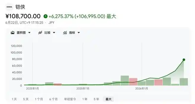
KIOXIA's stock price trend since listing

The Super Myth in the Capital Markets

KIOXIA successfully listed on the Tokyo Stock Exchange at the end of 2024, with its initial market capitalization hovering around only 800 billion yen (approximately $50 billion). However, with the comprehensive explosion of AI storage demand, KIOXIA performed an epic reversal in the 18 months following its listing: its stock price skyrocketed over 50 times within 18 months, rising 8-fold in 2026 alone.

Currently, KIOXIA's market capitalization has exceeded 51 trillion yen (approximately 481 trillion Korean won), repeatedly surpassing Toyota Motor, the symbol of Japanese manufacturing, to become the highest-valued company on the Japanese stock market.

According to KIOXIA's Q1 FY2026 (April–June) earnings forecast, its quarterly operating profit is expected to reach as high as 1.3 trillion yen (approximately $81 billion), a staggering increase of nearly 30 times year-over-year; the quarterly net profit guidance is 869 billion yen, a 48-fold increase year-over-year. The performance of a single quarter surpassed the full-year net profit forecast for FY2025.

As major customers scrambled to sign long-term supply contracts, KIOXIA's 2026 NAND capacity has been completely sold out, and the supply-demand imbalance is expected to persist until 2027. The market anticipates KIOXIA's operating profit margin this year to exceed 60%, setting a record for the highest profitability level in the global memory industry. Furthermore, with market expectations for shareholders to receive returns such as stock splits and dividends, its target stock price is hoped to rise to 200,000 yen.

This wave of soaring value has delivered investment returns beyond imagination to parent company Bain Capital, which held on during the downturn, and indirect major shareholder SK Hynix.

According to the Financial Times, the AI boom has made Bain's 2018 acquisition of Toshiba Memory (now KIOXIA) one of the most profitable private equity deals in history. Bain Capital has realized profits by selling most of its shares, with returns exceeding $150 billion, a near 20x return on investment. Its flagship private equity fund is estimated to have gained over $8 billion in profit.

SK Hynix invested a total of 395 billion yen (approximately 3.9 trillion Korean won at the time) in Toshiba Memory in 2018 through a consortium involving Korea, the US, and Japan, among other forms. Currently, this consortium still holds an 18% stake in KIOXIA. With the surge in KIOXIA's stock price, SK Hynix has seen enormous paper gains, and the market expects the consortium's eventual total profit to far exceed $70 billion.

The former 'hot potato' instantly transformed into a 'super ATM'.

In the past, the benefits of artificial intelligence were mainly concentrated in GPU and HBM companies like NVIDIA and SK Hynix. HBM was the star on the AI training side, while NAND became a scarce resource in AI inference, model storage, data lakes, enterprise SSDs, and nearline storage. The market expects KIOXIA's net profit for FY2027 to reach 2.8389 trillion yen, a 5.1-fold increase compared to the previous year.

3D NAND, The Foundation of KIOXIA's Existence

KIOXIA invented NAND flash memory over 35 years ago. In 2007, KIOXIA introduced BiCS FLASH 3D flash memory, a 3D flash memory technology system centered around vertical stacking, lateral scaling, wafer bonding, select gate optimization, and advanced packaging.

The basic idea of 3D NAND is: unlike 2D NAND, which only shrinks cells on a plane, it stacks memory cells vertically like building a skyscraper. KIOXIA's explanation is vivid: originally it was one floor with limited land area; 3D NAND is equivalent to turning a one-story building into a multi-story apartment, accommodating more 'residents' on the same area.

The core of BiCS FLASH is its batch processing technology. Its general process logic is: first, alternately stack plate-like electrodes and insulating layers; then drill a large number of holes along the vertical direction in one go; next, fill the holes with charge storage films and pillar-like electrodes; the intersection of the plate-like electrode and pillar-like electrode forms a memory cell. This shows that KIOXIA's BiCS FLASH is not the traditional 'create memory cells separately for each added layer,' but rather stacks the structure first, then forms memory cells by 'punching and plugging' through multiple layers at once. Therefore, when the number of layers increases, the manufacturing cost does not rise completely linearly, improving the economic viability of continued stacking for 3D NAND.

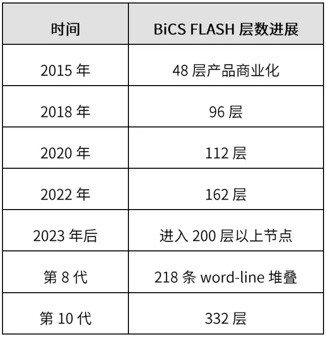
KIOXIA's officially disclosed commercialization timeline for BiCS FLASH is roughly as follows: BiCS FLASH products achieved commercialization with 48 layers in 2015, then progressed to 96 layers, 112 layers, 162 layers; as of March 2023, stacking of over 200 layers has been achieved.

Among these, the 8th-generation BiCS FLASH is a key milestone. KIOXIA states that the 8th-generation product uses 218 word-line stacks, achieves a storage density of 18.3Gb/mm² for the 1Tb TLC product, and supports a 3.2Gbps external data transfer speed, 40μs read time, and 205MB/s programming throughput.

KIOXIA's 8th-generation BiCS FLASH not only jumped from 162 layers to 218 layers but also introduced two key technologies:

CBA (CMOS directly Bonded to Array): CBA can be understood as manufacturing the peripheral CMOS control circuit and the memory array separately, followed by wafer bonding. In the past, CMOS circuits and the memory array were manufactured on the same wafer. However, the optimal process conditions for both are not identical: the memory array may require processes better suited for charge storage and stacked structures, while CMOS circuits focus more on logic control, electrical performance, and speed. Manufacturing them on the same wafer forces compromises.

CBA's approach is: manufacture the CMOS wafer separately, manufacture the memory array wafer separately, optimize the processes for each independently, and finally bond them together with high precision. The benefits are: improved bit density, increased NAND I/O speed, allowing the memory array to use high-temperature processes previously limited by CMOS constraints, and reduced electrical interference between adjacent memory cells.

OPS (On Pitch Select Gate): OPS solves the problem of wasted space within the memory array. In traditional structures, there exist 'dummy' areas between memory cells that are not used for data storage. These areas do not directly contribute to capacity but occupy area. KIOXIA's OPS technology, by rearranging select gates and insulating isolation structures, reduces or eliminates these ineffective areas, allowing more effective memory cells to be placed in the same area. KIOXIA's official explanation states that OPS removes unnecessary dummy regions, enabling more actual memory cells to be placed in the same space, significantly improving storage density.
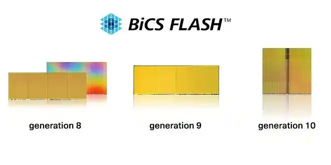
The 9th-generation BiCS FLASH primarily targets 512Gb and 1Tb TLC products, positioned to support applications in the mid-to-low capacity range that require high performance and low power consumption. It continues to use CBA and OPS technologies to improve production efficiency and provide more advanced flash memory solutions. The 9th generation does not follow the route of increasing layer count but emphasizes the balance between performance, power consumption, cost, and production efficiency.

The 10th-generation BiCS FLASH clearly leans more towards future high-capacity, high-performance demands. KIOXIA states that the 10th-generation product uses the same CMOS technology as the 9th generation while increasing the number of memory layers to 332, approximately 1.5 times that of the 8th generation, to enhance bit density and power efficiency.
Beyond front-end manufacturing processes, KIOXIA is also advancing back-end packaging capabilities. Official materials mention that KIOXIA developed a single-package 8TB flash memory, achieved by stacking 32 flash memory dies, each 2Tb, within one package. This relies on advanced back-end processes like wafer thinning, material design, and wire bonding. This 32-die stacking can assemble 32 pieces of 2Tb dies into a package with a height under 2mm, forming an 8TB flash memory solution.

From 3D NAND to 3D DRAM, KIOXIA's New Gambit

KIOXIA is also deploying a secret weapon to break through the single-product-line barrier of being a 'pure NAND vendor.' Why is KIOXIA venturing into 3D DRAM? This is because DRAM has also reached a planar scaling bottleneck similar to what NAND faced. As an established player in 3D NAND, KIOXIA also possesses process-validated advantages.

Continued scaling of traditional DRAM encounters several challenges: storage capacitors become increasingly difficult to shrink, access transistor leakage increases, data retention time shortens, refresh frequency rises, and higher capacity leads to higher refresh power consumption. Imec also mentioned in a technology review that the traditional DRAM 1T1C structure faces scaling, cost, and power efficiency challenges, especially as large capacitors limit the 3D integration path, and smaller transistors lead to more pronounced leakage paths, causing increased refresh power consumption.

In December 2024, KIOXIA announced the development of OCTRAM (Oxide-Semiconductor Channel Transistor DRAM) technology, a new 4F² DRAM composed of oxide semiconductor transistors, offering both high on-current and ultra-low off-current. This achievement was jointly developed by KIOXIA and Nanya Technology and presented at the 2024 IEEE IEDM.
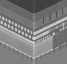
Panoramic view of OCTRAM (Source: KIOXIA, same below)

Traditional DRAM cells are generally 1T1C, meaning one access transistor plus one capacitor. Its problem is: as the cell continues to shrink, the capacitor becomes harder to make, and transistor leakage also increases refresh power consumption. KIOXIA's OCTRAM attempts to reduce leakage through InGaZnO transistors and push the cell structure towards higher density.
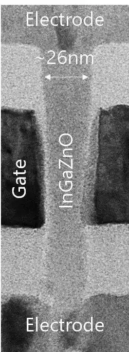
Cross-sectional TEM image of the InGaZnO vertical transistor

Due to its large bandgap and high electron mobility, InGaZnO transistors can theoretically achieve both ultra-low leakage and high on-current. KIOXIA, by optimizing contact electrode materials and spacer thickness, experimentally achieved over 15μA on-current while also realizing ultra-low leakage current below 10⁻¹⁸ A (as shown in the figure below). A significant portion of DRAM power consumption comes from refresh. Lower leakage leads to longer data retention time, reducing refresh pressure. Therefore, the core value of OCTRAM is using low-leakage oxide semiconductor transistors to reduce DRAM refresh power consumption.
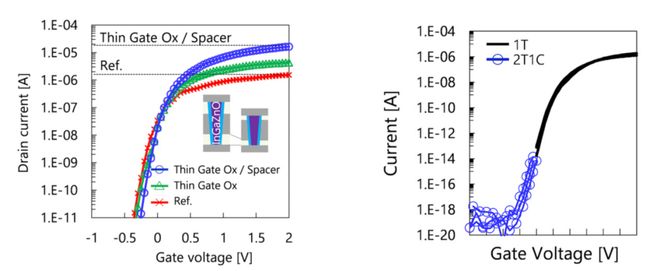
(a) On-current characteristics and (b) Off-current characteristics of the developed InGaZnO transistor

In September 2025, KIOXIA disclosed further reliability research on OCTRAM, focusing on TDDB lifetime issues of sub-25nm Gate-All-Around vertical InGaZnO transistors. TDDB stands for Time-Dependent Dielectric Breakdown. Simply put, it's whether the transistor's insulating layer gradually degrades and eventually fails under long-term electric field stress. KIOXIA stated they found lifetime degradation stems from two factors: intrinsic factors from scaling and extrinsic factors from the manufacturing process. By optimizing the process and reducing extrinsic degradation, KIOXIA achieved a projected TDDB lifetime exceeding 10 years.

In December 2025, KIOXIA announced progress closer to the core of 3D DRAM: developing oxide-semiconductor channel transistors capable of high stacking, having fabricated 8-layer horizontal transistor stacks with on-current exceeding 30μA and off-current below 1 aA, i.e., 10⁻¹⁸ A.

As of now, KIOXIA's 3D DRAM remains in the forefront R&D stage, not yet a commercial product.

KIOXIA is not a traditional DRAM giant, but its accumulated expertise in stacking processes, material integration, and array manufacturing from 3D NAND may give it an entry point in exploring next-generation 3D DRAM. Semiconductor Engineering also analyzed that KIOXIA's 3D DRAM path leverages mature oxide/nitride stacking capabilities from NAND to achieve lower-cost bit scaling, then uses IGZO to replace the channel to reduce thermal degradation issues.

However, one crucial point to emphasize is: KIOXIA's 3D DRAM is not HBM. HBM is packaging-level 3D; it stacks already manufactured DRAM dies to address high-bandwidth needs next to GPUs. KIOXIA's 3D DRAM is device/cell-level 3D; it aims to solve the problem of scaling the DRAM cell itself. Therefore, KIOXIA is not directly chasing HBM but is exploring a more fundamental 3D DRAM device path. If this path matures in the future, it may open a new technology branch for high-capacity, low-power working memory in the AI era.

Although 3D DRAM is still far from true commercialization. It currently resembles more of a future-facing technology ticket than an immediate revenue-contributing product line. But for KIOXIA, the significance of this ticket is not small. In the short term, KIOXIA can capitalize on the NAND recovery driven by AI; in the medium term, it advances high-layer BiCS FLASH; and in the long term, it bets on 3D DRAM, extending its 3D stacking capabilities from NAND to DRAM.

Conclusion

From massive losses and merger deadlock to the super myth of surpassing Toyota to become Japan's top-valued company in 2026, KIOXIA's rollercoaster trajectory is almost filled with the brutality and allure of the semiconductor memory industry. It was once cold-shouldered by capital markets for its single product line and missing the HBM wave, yet amid the tsunami of 'massive data flow' triggered by AI large models, it ushered in its own golden era by steadfastly adhering to NAND flash memory.

KIOXIA's comeback may not yet prove that Japanese semiconductors have truly revived. But at least it demonstrates one thing: in the semiconductor industry, a low point does not necessarily lead to exit. As long as technological assets remain, the realignment of cycles, capital, and demand can at any time bring a forgotten company back to the center of the table.

For KIOXIA, finding a long-term balance between fervent capital追捧 (pursuit) and the冷酷 (harsh) industry cycles moving forward will determine whether this lone sprout carrying the hopes of Japanese semiconductor revival is merely a fleeting flower in the AI supercycle or truly opens a new storage empire of its own.

*Disclaimer: This article was originally written by the author. The content represents the author's personal views. Semiconductor Industry Insights republishes it to convey a different perspective. This does not imply Semiconductor Industry Insights' agreement with or support for this view. If you have any objections, please contact Semiconductor Industry Insights.

Kripto yang Sedang Tren

Pertanyaan Terkait

QWhat triggered Kioxia's dramatic turnaround from a loss-making 'hot potato' to a stock market sensation in Japan?

AKioxia's dramatic turnaround was primarily triggered by the explosive demand for AI storage. The advent of large-scale AI models fundamentally shifted the market logic for memory. NAND flash, Kioxia's core product, became a scarce resource for AI inference, model storage, data lakes, enterprise SSDs, and nearline storage, leading to a supply shortage and surging profitability.

QWhat are the two key technologies (acronyms) introduced in Kioxia's 8th generation BiCS FLASH that significantly improved performance?

AThe two key technologies introduced in Kioxia's 8th generation BiCS FLASH are CBA (CMOS directly Bonded to Array) and OPS (On Pitch Select Gate). CBA improves density and speed by bonding separately optimized CMOS and array wafers, while OPS increases storage density by eliminating dummy areas within the memory array.

QWhat is the main technical advantage of Kioxia's OCTRAM (3D DRAM) technology over traditional DRAM?

AThe main technical advantage of Kioxia's OCTRAM technology is its use of InGaZnO (Oxide-Semiconductor) transistors, which offer extremely low leakage current (off-state current). This dramatically reduces refresh power consumption, a major challenge for traditional DRAM as it scales down, thereby enabling higher density and lower power 3D DRAM architectures.

QHow does Kioxia's approach to 3D DRAM (OCTRAM) fundamentally differ from High Bandwidth Memory (HBM)?

AKioxia's 3D DRAM (OCTRAM) is a device/cell-level 3D technology that aims to solve the fundamental scaling problems of the DRAM memory cell itself by stacking transistors vertically. In contrast, HBM is a package-level 3D technology that stacks pre-manufactured DRAM dies to achieve high bandwidth, primarily for GPU-adjacent memory. They address different layers of the memory hierarchy and scaling challenges.

QWhich major investors reaped enormous returns from Kioxia's stock surge, and what was the scale of one of their profits?

AThe major investors were Bain Capital (the parent company) and SK Hynix (an indirect major shareholder). Bain Capital's investment from the 2018 Toshiba Memory buyout became one of the most profitable private equity deals ever, with profits exceeding $15 billion and a return of nearly 20 times. The SK Hynix-led consortium is also expected to realize total profits far exceeding $70 billion.

Bacaan Terkait

Trading

Spot

Artikel Populer

Apa Itu $S$

Memahami SPERO: Tinjauan Komprehensif Pengenalan SPERO Seiring dengan perkembangan lanskap inovasi, munculnya teknologi web3 dan proyek cryptocurrency memainkan peran penting dalam membentuk masa depan digital. Salah satu proyek yang telah menarik perhatian di bidang dinamis ini adalah SPERO, yang dilambangkan sebagai SPERO,$$s$. Artikel ini bertujuan untuk mengumpulkan dan menyajikan informasi terperinci tentang SPERO, untuk membantu para penggemar dan investor memahami dasar-dasar, tujuan, dan inovasi dalam domain web3 dan crypto. Apa itu SPERO,$$s$? SPERO,$$s$ adalah proyek unik dalam ruang crypto yang berusaha memanfaatkan prinsip desentralisasi dan teknologi blockchain untuk menciptakan ekosistem yang mendorong keterlibatan, utilitas, dan inklusi finansial. Proyek ini dirancang untuk memfasilitasi interaksi peer-to-peer dengan cara baru, memberikan pengguna solusi dan layanan keuangan yang inovatif. Pada intinya, SPERO,$$s$ bertujuan untuk memberdayakan individu dengan menyediakan alat dan platform yang meningkatkan pengalaman pengguna dalam ruang cryptocurrency. Ini termasuk memungkinkan metode transaksi yang lebih fleksibel, mendorong inisiatif yang dipimpin komunitas, dan menciptakan jalur untuk peluang finansial melalui aplikasi terdesentralisasi (dApps). Visi mendasar dari SPERO,$$s$ berputar di sekitar inklusivitas, bertujuan untuk menjembatani kesenjangan dalam keuangan tradisional sambil memanfaatkan manfaat teknologi blockchain. Siapa Pencipta SPERO,$$s$? Identitas pencipta SPERO,$$s$ tetap agak samar, karena ada sumber daya publik yang terbatas yang memberikan informasi latar belakang terperinci tentang pendiriannya. Kurangnya transparansi ini dapat berasal dari komitmen proyek terhadap desentralisasi—sebuah etos yang banyak proyek web3 bagi, memprioritaskan kontribusi kolektif di atas pengakuan individu. Dengan memusatkan diskusi di sekitar komunitas dan tujuan kolektifnya, SPERO,$$s$ mewujudkan esensi pemberdayaan tanpa menonjolkan individu tertentu. Dengan demikian, memahami etos dan misi SPERO tetap lebih penting daripada mengidentifikasi pencipta tunggal. Siapa Investor SPERO,$$s$? SPERO,$$s$ didukung oleh beragam investor mulai dari modal ventura hingga investor malaikat yang berdedikasi untuk mendorong inovasi di sektor crypto. Fokus investor ini umumnya sejalan dengan misi SPERO—memprioritaskan proyek yang menjanjikan kemajuan teknologi sosial, inklusivitas finansial, dan tata kelola terdesentralisasi. Fondasi investor ini biasanya tertarik pada proyek yang tidak hanya menawarkan produk inovatif tetapi juga memberikan kontribusi positif kepada komunitas blockchain dan ekosistemnya. Dukungan dari investor ini memperkuat SPERO,$$s$ sebagai pesaing yang patut diperhitungkan di domain proyek crypto yang berkembang pesat. Bagaimana SPERO,$$s$ Bekerja? SPERO,$$s$ menerapkan kerangka kerja multi-faceted yang membedakannya dari proyek cryptocurrency konvensional. Berikut adalah beberapa fitur kunci yang menekankan keunikan dan inovasinya: Tata Kelola Terdesentralisasi: SPERO,$$s$ mengintegrasikan model tata kelola terdesentralisasi, memberdayakan pengguna untuk berpartisipasi aktif dalam proses pengambilan keputusan mengenai masa depan proyek. Pendekatan ini mendorong rasa kepemilikan dan akuntabilitas di antara anggota komunitas. Utilitas Token: SPERO,$$s$ memanfaatkan token cryptocurrency-nya sendiri, yang dirancang untuk melayani berbagai fungsi dalam ekosistem. Token ini memungkinkan transaksi, hadiah, dan fasilitasi layanan yang ditawarkan di platform, meningkatkan keterlibatan dan utilitas secara keseluruhan. Arsitektur Berlapis: Arsitektur teknis SPERO,$$s$ mendukung modularitas dan skalabilitas, memungkinkan integrasi fitur dan aplikasi tambahan secara mulus seiring dengan perkembangan proyek. Kemampuan beradaptasi ini sangat penting untuk mempertahankan relevansi di lanskap crypto yang selalu berubah. Keterlibatan Komunitas: Proyek ini menekankan inisiatif yang dipimpin komunitas, menggunakan mekanisme yang memberikan insentif untuk kolaborasi dan umpan balik. Dengan memelihara komunitas yang kuat, SPERO,$$s$ dapat lebih baik memenuhi kebutuhan pengguna dan beradaptasi dengan tren pasar. Fokus pada Inklusi: Dengan menawarkan biaya transaksi yang rendah dan antarmuka yang ramah pengguna, SPERO,$$s$ bertujuan untuk menarik basis pengguna yang beragam, termasuk individu yang mungkin sebelumnya tidak terlibat dalam ruang crypto. Komitmen ini terhadap inklusi sejalan dengan misi utamanya untuk memberdayakan melalui aksesibilitas. Garis Waktu SPERO,$$s$ Memahami sejarah proyek memberikan wawasan penting tentang trajektori dan tonggak perkembangannya. Berikut adalah garis waktu yang disarankan yang memetakan peristiwa signifikan dalam evolusi SPERO,$$s$: Fase Konseptualisasi dan Ideasi: Ide awal yang membentuk dasar SPERO,$$s$ dikembangkan, sangat selaras dengan prinsip desentralisasi dan fokus komunitas dalam industri blockchain. Peluncuran Whitepaper Proyek: Setelah fase konseptual, whitepaper komprehensif yang merinci visi, tujuan, dan infrastruktur teknologi SPERO,$$s$ dirilis untuk menarik minat dan umpan balik komunitas. Pembangunan Komunitas dan Keterlibatan Awal: Upaya jangkauan aktif dilakukan untuk membangun komunitas pengguna awal dan investor potensial, memfasilitasi diskusi seputar tujuan proyek dan mendapatkan dukungan. Acara Generasi Token: SPERO,$$s$ melakukan acara generasi token (TGE) untuk mendistribusikan token asli kepada pendukung awal dan membangun likuiditas awal dalam ekosistem. Peluncuran dApp Awal: Aplikasi terdesentralisasi (dApp) pertama yang terkait dengan SPERO,$$s$ diluncurkan, memungkinkan pengguna untuk terlibat dengan fungsionalitas inti platform. Pengembangan Berkelanjutan dan Kemitraan: Pembaruan dan peningkatan berkelanjutan terhadap penawaran proyek, termasuk kemitraan strategis dengan pemain lain di ruang blockchain, telah membentuk SPERO,$$s$ menjadi pemain yang kompetitif dan berkembang di pasar crypto. Kesimpulan SPERO,$$s$ berdiri sebagai bukti potensi web3 dan cryptocurrency untuk merevolusi sistem keuangan dan memberdayakan individu. Dengan komitmen terhadap tata kelola terdesentralisasi, keterlibatan komunitas, dan fungsionalitas yang dirancang secara inovatif, ia membuka jalan menuju lanskap keuangan yang lebih inklusif. Seperti halnya investasi di ruang crypto yang berkembang pesat, calon investor dan pengguna dianjurkan untuk melakukan riset secara menyeluruh dan terlibat dengan perkembangan yang sedang berlangsung dalam SPERO,$$s$. Proyek ini menunjukkan semangat inovatif industri crypto, mengundang eksplorasi lebih lanjut ke dalam berbagai kemungkinan yang ada. Meskipun perjalanan SPERO,$$s$ masih berlangsung, prinsip-prinsip dasarnya mungkin benar-benar mempengaruhi masa depan cara kita berinteraksi dengan teknologi, keuangan, dan satu sama lain dalam ekosistem digital yang saling terhubung.

109 Total TayanganDipublikasikan pada 2024.12.17Diperbarui pada 2024.12.17

Apa Itu $S$

Apa Itu AGENT S

Agent S: Masa Depan Interaksi Otonom di Web3 Pendahuluan Dalam lanskap Web3 dan cryptocurrency yang terus berkembang, inovasi secara konstan mendefinisikan ulang cara individu berinteraksi dengan platform digital. Salah satu proyek perintis, Agent S, menjanjikan untuk merevolusi interaksi manusia-komputer melalui kerangka agen terbuka. Dengan membuka jalan untuk interaksi otonom, Agent S bertujuan untuk menyederhanakan tugas-tugas kompleks, menawarkan aplikasi transformasional dalam kecerdasan buatan (AI). Eksplorasi mendetail ini akan menyelami seluk-beluk proyek, fitur uniknya, dan implikasinya untuk domain cryptocurrency. Apa itu Agent S? Agent S berdiri sebagai kerangka agen terbuka yang inovatif, dirancang khusus untuk mengatasi tiga tantangan mendasar dalam otomatisasi tugas komputer: Memperoleh Pengetahuan Spesifik Domain: Kerangka ini secara cerdas belajar dari berbagai sumber pengetahuan eksternal dan pengalaman internal. Pendekatan ganda ini memberdayakannya untuk membangun repositori pengetahuan spesifik domain yang kaya, meningkatkan kinerjanya dalam pelaksanaan tugas. Perencanaan Selama Rentang Tugas yang Panjang: Agent S menggunakan perencanaan hierarkis yang ditingkatkan pengalaman, pendekatan strategis yang memfasilitasi pemecahan dan pelaksanaan tugas-tugas rumit dengan efisien. Fitur ini secara signifikan meningkatkan kemampuannya untuk mengelola beberapa subtugas dengan efisien dan efektif. Menangani Antarmuka Dinamis dan Tidak Seragam: Proyek ini memperkenalkan Antarmuka Agen-Komputer (ACI), solusi inovatif yang meningkatkan interaksi antara agen dan pengguna. Dengan memanfaatkan Model Bahasa Besar Multimodal (MLLM), Agent S dapat menavigasi dan memanipulasi berbagai antarmuka pengguna grafis dengan mulus. Melalui fitur-fitur perintis ini, Agent S menyediakan kerangka kerja yang kuat yang mengatasi kompleksitas yang terlibat dalam mengotomatisasi interaksi manusia dengan mesin, membuka jalan untuk berbagai aplikasi dalam AI dan seterusnya. Siapa Pencipta Agent S? Meskipun konsep Agent S secara fundamental inovatif, informasi spesifik tentang penciptanya tetap samar. Pencipta saat ini tidak diketahui, yang menyoroti baik tahap awal proyek atau pilihan strategis untuk menjaga anggota pendiri tetap tersembunyi. Terlepas dari anonimitas, fokus tetap pada kemampuan dan potensi kerangka kerja. Siapa Investor Agent S? Karena Agent S relatif baru dalam ekosistem kriptografi, informasi terperinci mengenai investor dan pendukung keuangannya tidak secara eksplisit didokumentasikan. Kurangnya wawasan yang tersedia untuk umum mengenai fondasi investasi atau organisasi yang mendukung proyek ini menimbulkan pertanyaan tentang struktur pendanaannya dan peta jalan pengembangannya. Memahami dukungan sangat penting untuk mengukur keberlanjutan proyek dan potensi dampak pasar. Bagaimana Cara Kerja Agent S? Di inti Agent S terletak teknologi mutakhir yang memungkinkannya berfungsi secara efektif dalam berbagai pengaturan. Model operasionalnya dibangun di sekitar beberapa fitur kunci: Interaksi Komputer yang Mirip Manusia: Kerangka ini menawarkan perencanaan AI yang canggih, berusaha untuk membuat interaksi dengan komputer lebih intuitif. Dengan meniru perilaku manusia dalam pelaksanaan tugas, ia menjanjikan untuk meningkatkan pengalaman pengguna. Memori Naratif: Digunakan untuk memanfaatkan pengalaman tingkat tinggi, Agent S memanfaatkan memori naratif untuk melacak sejarah tugas, sehingga meningkatkan proses pengambilan keputusannya. Memori Episodik: Fitur ini memberikan panduan langkah demi langkah kepada pengguna, memungkinkan kerangka untuk menawarkan dukungan kontekstual saat tugas berlangsung. Dukungan untuk OpenACI: Dengan kemampuan untuk berjalan secara lokal, Agent S memungkinkan pengguna untuk mempertahankan kontrol atas interaksi dan alur kerja mereka, sejalan dengan etos terdesentralisasi Web3. Integrasi Mudah dengan API Eksternal: Versatilitas dan kompatibilitasnya dengan berbagai platform AI memastikan bahwa Agent S dapat dengan mulus masuk ke dalam ekosistem teknologi yang ada, menjadikannya pilihan menarik bagi pengembang dan organisasi. Fungsionalitas ini secara kolektif berkontribusi pada posisi unik Agent S dalam ruang kripto, saat ia mengotomatisasi tugas-tugas kompleks yang melibatkan banyak langkah dengan intervensi manusia yang minimal. Seiring proyek ini berkembang, aplikasi potensialnya di Web3 dapat mendefinisikan ulang bagaimana interaksi digital berlangsung. Garis Waktu Agent S Pengembangan dan tonggak Agent S dapat dirangkum dalam garis waktu yang menyoroti peristiwa pentingnya: 27 September 2024: Konsep Agent S diluncurkan dalam sebuah makalah penelitian komprehensif berjudul “Sebuah Kerangka Agen Terbuka yang Menggunakan Komputer Seperti Manusia,” yang menunjukkan dasar untuk proyek ini. 10 Oktober 2024: Makalah penelitian tersebut dipublikasikan secara terbuka di arXiv, menawarkan eksplorasi mendalam tentang kerangka kerja dan evaluasi kinerjanya berdasarkan tolok ukur OSWorld. 12 Oktober 2024: Sebuah presentasi video dirilis, memberikan wawasan visual tentang kemampuan dan fitur Agent S, lebih lanjut melibatkan pengguna dan investor potensial. Tanda-tanda dalam garis waktu ini tidak hanya menggambarkan kemajuan Agent S tetapi juga menunjukkan komitmennya terhadap transparansi dan keterlibatan komunitas. Poin Kunci Tentang Agent S Seiring kerangka Agent S terus berkembang, beberapa atribut kunci menonjol, menekankan sifat inovatif dan potensinya: Kerangka Inovatif: Dirancang untuk memberikan penggunaan komputer yang intuitif seperti interaksi manusia, Agent S membawa pendekatan baru untuk otomatisasi tugas. Interaksi Otonom: Kemampuan untuk berinteraksi secara otonom dengan komputer melalui GUI menandakan lompatan menuju solusi komputasi yang lebih cerdas dan efisien. Otomatisasi Tugas Kompleks: Dengan metodologinya yang kuat, ia dapat mengotomatisasi tugas-tugas kompleks yang melibatkan banyak langkah, membuat proses lebih cepat dan kurang rentan terhadap kesalahan. Perbaikan Berkelanjutan: Mekanisme pembelajaran memungkinkan Agent S untuk belajar dari pengalaman masa lalu, terus meningkatkan kinerja dan efektivitasnya. Versatilitas: Adaptabilitasnya di berbagai lingkungan operasi seperti OSWorld dan WindowsAgentArena memastikan bahwa ia dapat melayani berbagai aplikasi. Saat Agent S memposisikan dirinya di lanskap Web3 dan kripto, potensinya untuk meningkatkan kemampuan interaksi dan mengotomatisasi proses menandakan kemajuan signifikan dalam teknologi AI. Melalui kerangka inovatifnya, Agent S mencerminkan masa depan interaksi digital, menjanjikan pengalaman yang lebih mulus dan efisien bagi pengguna di berbagai industri. Kesimpulan Agent S mewakili lompatan berani ke depan dalam pernikahan AI dan Web3, dengan kapasitas untuk mendefinisikan ulang cara kita berinteraksi dengan teknologi. Meskipun masih dalam tahap awal, kemungkinan aplikasinya sangat luas dan menarik. Melalui kerangka komprehensifnya yang mengatasi tantangan kritis, Agent S bertujuan untuk membawa interaksi otonom ke garis depan pengalaman digital. Saat kita melangkah lebih dalam ke dalam ranah cryptocurrency dan desentralisasi, proyek-proyek seperti Agent S pasti akan memainkan peran penting dalam membentuk masa depan teknologi dan kolaborasi manusia-komputer.

956 Total TayanganDipublikasikan pada 2025.01.14Diperbarui pada 2025.01.14

Apa Itu AGENT S

Cara Membeli S

Selamat datang di HTX.com! Kami telah membuat pembelian Sonic (S) menjadi mudah dan nyaman. Ikuti panduan langkah demi langkah kami untuk memulai perjalanan kripto Anda.Langkah 1: Buat Akun HTX AndaGunakan alamat email atau nomor ponsel Anda untuk mendaftar akun gratis di HTX. Rasakan perjalanan pendaftaran yang mudah dan buka semua fitur.Dapatkan Akun SayaLangkah 2: Buka Beli Kripto, lalu Pilih Metode Pembayaran AndaKartu Kredit/Debit: Gunakan Visa atau Mastercard Anda untuk membeli Sonic (S) secara instan.Saldo: Gunakan dana dari saldo akun HTX Anda untuk melakukan trading dengan lancar.Pihak Ketiga: Kami telah menambahkan metode pembayaran populer seperti Google Pay dan Apple Pay untuk meningkatkan kenyamanan.P2P: Lakukan trading langsung dengan pengguna lain di HTX.Over-the-Counter (OTC): Kami menawarkan layanan yang dibuat khusus dan kurs yang kompetitif bagi para trader.Langkah 3: Simpan Sonic (S) AndaSetelah melakukan pembelian, simpan Sonic (S) di akun HTX Anda. Selain itu, Anda dapat mengirimkannya ke tempat lain melalui transfer blockchain atau menggunakannya untuk memperdagangkan mata uang kripto lainnya.Langkah 4: Lakukan trading Sonic (S)Lakukan trading Sonic (S) dengan mudah di pasar spot HTX. Cukup akses akun Anda, pilih pasangan perdagangan, jalankan trading, lalu pantau secara real-time. Kami menawarkan pengalaman yang ramah pengguna baik untuk pemula maupun trader berpengalaman.

1.6k Total TayanganDipublikasikan pada 2025.01.15Diperbarui pada 2026.06.02

Cara Membeli S

Diskusi

Selamat datang di Komunitas HTX. Di sini, Anda bisa terus mendapatkan informasi terbaru tentang perkembangan platform terkini dan mendapatkan akses ke wawasan pasar profesional. Pendapat pengguna mengenai harga S (S) disajikan di bawah ini.

活动图片