From Computing to Storage: The Two-Dimensional Semiconductor Industry Chain is Taking Shape

marsbitОпубликовано 2026-07-29Обновлено 2026-07-29

Введение

The article "From Computing to Storage: The 2D Semiconductor Industry Chain is Taking Shape" discusses the rise of two-dimensional (2D) semiconductors as a pivotal material in the post-Moore era. As silicon-based chips approach physical limits, 2D semiconductors like molybdenum disulfide (MoS2), offer atomic-layer thinness and superior electrical properties, making them a promising non-silicon alternative for advanced nodes beyond 1nm. Globally, industry leaders like TSMC, Intel, and Samsung, along with research institutes like IMEC, are actively investing in this field. Domestically in China, significant progress is being made across the entire supply chain, from material production and equipment R&D to chip integration and ecosystem development. **Key highlights include:** * **Material & Equipment Breakthroughs:** Chinese research teams and companies like Jimo Xin Technology have achieved mass production of 6-inch and 8-inch 2D semiconductor single-crystal wafers using domestically developed equipment like Oxy-MOCVD. This addresses the critical challenge of large-area, high-quality material growth. Breakthroughs have also been made in p-type 2D materials (e.g., MoSi2N4) and wafer-scale ferroelectric thin films, essential for building complementary circuits and low-power transistors. * **Engineering Ecosystem Formation:** A landmark 8-inch 2D semiconductor pilot line in Pudong has become fully operational, bridging the gap between lab research and industrial manufactu...

Two-dimensional (2D) semiconductors, also known as atomic layer semiconductors, are semiconductor materials whose core functional layers are only a single or a few atomic layers thick. Represented by transition metal dichalcogenides (e.g., molybdenum disulfide), they are among the key materials for the post-Moore era. As silicon-based chip manufacturing processes approach physical limits, traditional silicon channel semiconductor materials are nearing their performance ceiling. 2D semiconductors (such as MoS2, WSe2, InSe), leveraging their inherent advantage of atomic-level thickness, can achieve natural strong gate control at short-channel scales with wafer-scale atomically flat structures, and are regarded as the most promising non-silicon new material for the post-Moore era.

Currently, a global industrial consensus is rapidly forming. Leading international wafer manufacturing giants like TSMC, Intel, and Samsung, as well as top research institutions such as IMEC and IRDS, have all explicitly positioned themselves in the 2D semiconductor field, judging that they will be integrated as core components into heterogeneous integration systems after the 1nm node. In June 2026, TSMC, in collaboration with ASML and imec, demonstrated for the first time at the VLSI Symposium the integration of 2D n/pFETs with a 50 nm gate-contact pitch on a 300 mm wafer, signifying that international giants are accelerating the push for 2D transistors from lab to fab. In this context, the domestic industry chain has also accelerated full-chain layout, achieving breakthroughs from material preparation and equipment self-development to chip integration and ecosystem construction. The 2D semiconductor industry chain is taking shape.

01 Material Breakthroughs and Equipment Autonomy: From 'Can Make' to 'Can Produce'

2D semiconductors are considered key materials for post-silicon chip manufacturing, but the large-scale, high-quality wafer preparation of 2D semiconductor materials is a prerequisite for their industrial application. Among them, Chemical Vapor Deposition (CVD) and Metal-Organic Chemical Vapor Deposition (MOCVD) are key technologies for future large-scale manufacturing of 2D semiconductor materials.
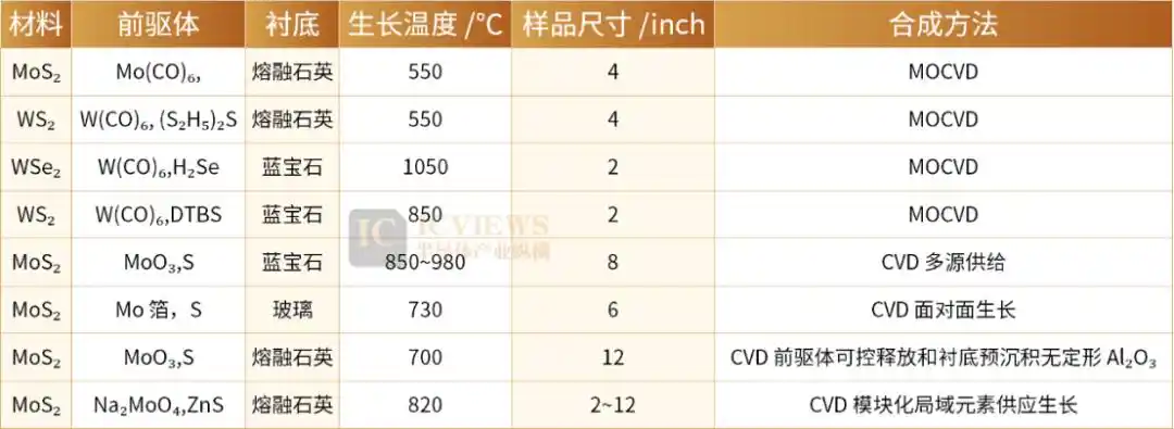
In the field of equipment and material growth, a team led by Professor Wang Xinran from Nanjing University, in collaboration with its industrial transformation platform Jimoxin Technology, has formed a deep closed-loop integration of "academic innovation—equipment development—process verification," achieving a series of advancements in wafer-scale 2D semiconductor single-crystal preparation. In October 2025, leveraging the Oxy-MOCVD 200 ultra equipment (with 100% domestic core components) independently developed by Jimoxin Technology, and through innovative substrate engineering techniques, the team reported for the first time globally the mass-production preparation of the world's first 6-inch 2D transition metal dichalcogenide semiconductor single crystal, compatible with materials like MoS2, WS2, and WSe2, with a unidirectional domain alignment rate exceeding 99% on a 150 mm wafer. In January 2026, collaborating with Professor Wang Jinlan's team from Southeast University, they developed a novel Oxygen-assisted Metal-Organic Chemical Vapor Deposition (oxy-MOCVD) technology, breaking through the bottleneck of growth kinetics control. This not only increased the average domain size of MoS2 crystals from the hundred-nanometer scale to hundreds of micrometers, solving the mass-production challenge of large-area uniform growth, but also fundamentally suppressed carbon contamination issues. Based on this process, Jimoxin Technology completed in-depth customization and upgrades of its equipment, enabling plug-and-play process capabilities for downstream users. The current technology system covers mainstream 2D semiconductor materials like MoS2, MoSe2, WS2, and WSe2. Building on this, Jimoxin Technology has further achieved a global first by realizing mass production of 8-inch 2D semiconductor single crystals. Its products have entered top research institutions like the University of Cambridge and Fudan University, and collaborations have been established with downstream chip manufacturers, bridging the critical step from lab samples to production-grade materials.

Beyond mainstream n-type materials, the shortcoming in wafer-level preparation of p-type 2D semiconductors has also been addressed. Similar to silicon-based electronic devices, wafer-level n-type and p-type 2D semiconductor single crystals are the foundation and prerequisite for building 2D CMOS integrated circuits. To date, researchers have developed various n-type 2D semiconductor materials, among which MoS2 and WS2 have achieved wafer-scale single-crystal preparation. However, p-type 2D semiconductors combining high mobility and excellent stability remain scarce, and achieving wafer-level single-crystal growth of such materials is even more challenging. In July 2026, a team from the Institute of Metal Research, Chinese Academy of Sciences, made a breakthrough by successfully preparing large-area, high-performance p-type MoSi2N4 monolayer single-crystal wafers. This material system was pioneered by this team, previously only achievable as polycrystalline films where grain boundary gaps would significantly degrade device performance and cause damage during transfer processes. This research, through the step-guided effect of a special single-crystal substrate, achieved directional growth and seamless splicing of the material, finally filling the core gap of long-missing high-quality p-type materials for 2D CMOS circuits.

In the direction of specialty materials, a research team led by Professor Peng Hailin from Peking University achieved, for the first time, the controlled preparation of ultra-thin, uniform ferroelectric thin films and their heterostructures at the wafer scale. They constructed high-speed ferroelectric transistors with ultra-low operating voltage (0.8V) and extremely high endurance (surviving over 1.5×10^12 cycles). Their overall performance significantly surpasses existing industrial hafnium-based ferroelectric systems, representing the currently known ferroelectric transistor with the smallest operating voltage, lowest energy consumption, and best endurance. This marks the first international demonstration of a high-performance wafer-level 2D ferroelectric material system, providing a breakthrough material foundation and feasible technological pathway for developing high-efficiency advanced chips.

02 Engineering Ecosystem Gradually Forms, Bridging the Gap from Lab to Fab

Breakthroughs in materials and devices ultimately need to be integrated into standardized manufacturing systems.

On July 9, 2026, the 8-inch Two-Dimensional Semiconductor Engineering Demonstration Pilot Line, built by Yuanyiwei Technology, was fully operational in Pudong, becoming a milestone for China's 2D semiconductor transition from research to industrialization. This pilot line achieved first light in January 2026 and, in just over half a year, completed full-process equipment debugging and process optimization. Differentiating itself from small-scale lab trial platforms, it now possesses complete tape-out and engineering trial production capabilities, establishing a full engineering chain from material preparation to chip integration. Prior to this, domestic 2D semiconductor research was mostly concentrated in university labs, with device preparation relying on small-batch manual trials, leaving a significant gap from industrial standards. The Yuanyiwei team, after ten years of dedicated effort, has mastered the complete manufacturing process encompassing wafer growth, integration processes, device modeling, circuit design, and packaging/testing.

The accompanying Process Design Kit (PDK) has also been deployed, further bridging the gap between design and manufacturing. The PDK 0.1 version for 500 nm nodes based on the 8-inch pilot line, released by Yuanyiwei, is the first process IP in the 2D semiconductor field compatible with mainstream EDA toolchains. It includes a complete set of tools like Pcells, DRC, LVS, and PEX, with a process yield exceeding 99.99%. Various performance metrics break international records, basically approaching the level of silicon-based processes at equivalent nodes. In the future, it can support the design and wafer-level manufacturing of 2D circuits with up to 100,000 gates.

Accompanying the line's operation and PDK release, foundry services and the industrial ecosystem have been simultaneously launched. University teams from Peking University, Tsinghua University, Shanghai Jiao Tong University, Nanjing University, and others have completed R&D collaboration agreements with Yuanyiwei, officially opening wafer foundry services to the research community. Companies like Xi'an XianDao Institute and Shanghai 2D Star Technology have also formed strategic industry chain partnerships, engaging in deep collaboration around shared process platforms, technology transfer, and ecosystem co-construction. Local industrial support is also advancing in sync. Shanghai Chuansha New Town is leveraging the Yuanyiwei pilot line as a core carrier to attract upstream and downstream companies. At the Shanghai municipal level, 2D semiconductors have been incorporated as a key cultivation direction for future industries, with comprehensive efforts from R&D and collaborative innovation to ecosystem nurturing, aiming to form a complete industrial loop of "R&D—Pilot—Mass Production." Notably, approximately 70% of the equipment for a 2D semiconductor production line can be reused from existing silicon-based semiconductor equipment, meaning it will not overturn the existing industrial system. Instead, it will foster entirely new market increments in areas like materials, equipment, manufacturing, and advanced packaging.

03 Expanding Application Landscape: From Computing to Storage

With the maturation of the manufacturing system, 2D semiconductors are also expanding from logic computing to application scenarios like storage.

In the logic computing domain, China has completed the leap from devices to complex processors. In 2025, the world's first 32-bit RISC-V architecture microprocessor based on 2D semiconductor materials, named "Wuji," was released. It employs molybdenum disulfide (MoS2) material, integrates 5900 transistors, is only 0.7 nm thick, and achieves a single-stage inverter yield of 99.77%, realizing full-chain independent R&D from material and architecture to tape-out, verifying the feasibility of building complex logic circuits with 2D materials. This processor can serially execute 37 types of 32-bit RISC-V instructions at a 1kHz clock frequency, meeting the RV32I integer instruction set requirements. It features high single-stage gain and ultra-low off-state leakage current, suitable for scenarios like IoT and edge computing.

In 2026, teams led by Professors Wang Xinran and Qiu Hao from Nanjing University, in collaboration with Suzhou National Laboratory and Huawei, further integrated the full design-process-manufacturing flow for 2D semiconductor chips compatible with Fab production lines. They successfully developed the world's first MoS2 multi-bit parallel microprocessor, "Mengqi (MAGIC)-1000," setting a new record for transistor integration density in emerging non-silicon digital circuits. This marks China's entry into a new development stage of production line integration in 2D semiconductor research. Through cross-level co-optimization, the team integrated 1433 MoS2 transistors into an ultra-compact chip area using a 0.5μm industrial process, successfully developing the "MAGIC-1000" microprocessor. The chip employs a RISC instruction set and consists of four main modules: instruction decoder, register file, arithmetic logic unit, and multiplexer. Its integrated transistor density increased by an order of magnitude compared to the previous international record, reaching 9336/mm², comparable to mature silicon-based processes at the same node. The chip achieved multi-bit data parallel operation with 2D semiconductors for the first time, with a maximum operating frequency of 43 kHz. It also integrated an on-chip register file on the 2D chip, eliminating the access latency and bandwidth bottlenecks associated with off-chip memory.

In the storage domain, the ultra-low leakage characteristics of 2D semiconductors demonstrate unique strategic value. A joint team from Fudan University developed the 2D semiconductor transistor with the lowest leakage current to date. The team achieved a record-breaking ultra-low leakage current—equivalent to leaking only one electron every 9.15 seconds. Building on this, they created a novel DRAM memory chip that achieved an ultra-long data retention time exceeding 8500 seconds at zero hold voltage, while simultaneously maintaining high-speed read/write and multi-capacity storage capabilities. The optimized Capacitorless Two-Transistor DRAM (2T0C) achieved quasi-non-volatile memory operation, 5-bit storage precision, and nanosecond-level write speeds. Yuanyiwei has positioned DRAM as a key strategic direction. The ultra-low leakage of 2D semiconductors can significantly reduce refresh power consumption, promising early adoption in edge-side and high-compute-power scenarios, with future capacity enhancement through 3D stacking technology. In July 2026, the team of Professors Zhou Peng and Liu Chunsen from Fudan University went a step further. For the first time, they clearly observed non-volatile single-electron storage behavior at room temperature, successfully creating a device with the world's largest non-volatile quantum storage window—requiring the injection of only a single electron to achieve a storage window of 0.5 volts. This signifies that charge information storage technology has reached the pinnacle of "one electron, one bit."

Beyond computing and storage, 2D semiconductors possess irreplaceable advantages in more specialized scenarios. As an ultimate SOI material, 2D semiconductors have unique advantages in radio frequency (RF) analog circuits, radiation-hardened communications, brain-computer interfaces, etc. In January of this year, relying on the "Fudan-1" satellite platform, a 2D semiconductor radiation-hardened RF communication system achieved its first in-orbit space validation. Additionally, 2D semiconductors can be fabricated into flexible, transparent devices, supporting device R&D in cutting-edge fields like optoelectronic sensing and quantum computing.

04 Conclusion

Currently, 2D semiconductors have completely moved out of the laboratory, entering a new development stage of engineering verification and small-batch tape-outs. From wafer-level breakthroughs in material preparation, to the engineering operation of manufacturing lines, to application deployment in multiple fields like computing and storage, every link in China's domestic 2D semiconductor industry chain is accelerating. An initial complete industry chain covering materials, equipment, manufacturing, design, and application has taken shape.

In this emerging 2D semiconductor field, international competition is in full swing. The formation of this new industry chain not only provides new possibilities for chip technology in the post-Moore era but also opens a brand-new dimension of competition in the reshaping of the global semiconductor industry landscape.

This article is from the WeChat public account "Semiconductor Industry Review" (ID: ICViews), author: Peng Cheng


Трендовые криптовалюты

Связанные с этим вопросы

QWhat are 2D semiconductors and why are they considered a key material in the post-Moore era?

A2D semiconductors, also known as atomic-layer semiconductors, are materials with a core functional layer only one or a few atoms thick. Representative examples include transition metal dichalcogenides like molybdenum disulfide (MoS2). They are considered a key post-Moore material because, as silicon-based chip processes approach physical limits, 2D semiconductors offer natural advantages like atomic-level thickness and an atomically flat wafer-scale structure. This enables strong gate control at short channel lengths, positioning them as a highly promising non-silicon new material.

QWhat significant achievement did TSMC, ASML, and imec demonstrate regarding 2D semiconductor integration in 2026?

AIn June 2026, TSMC, in collaboration with ASML and imec, demonstrated the integration of 2D n/pFETs with a 50 nm contact gate pitch on a 300 mm wafer for the first time at the VLSI Symposium. This marked a significant step by international industry leaders in accelerating the transition of 2D transistors from laboratory research towards production lines.

QWhich company's team achieved the mass production of 6-inch single-crystal 2D semiconductor wafers using a domestically developed device?

AProfessor Wang Xinran's team from Nanjing University, in collaboration with its industrial transformation platform Jimo Xinke Technology, achieved this. Using their self-developed, 100% domestically sourced Oxy-MOCVD 200 ultra equipment, they reported the world's first mass-production preparation of 6-inch single-crystal 2D transition metal dichalcogenide semiconductors in October 2025.

QWhat major milestone did the 8-inch 2D semiconductor pilot line in Pudong represent for China's industry?

AThe full commissioning of the 8-inch 2D semiconductor engineering pilot line in Pudong, built by Yuanji Micro, in July 2026 represented a milestone for China's 2D semiconductor industry. It transitioned the technology from scientific research to industrialization, establishing complete wafer fabrication and engineering trial production capabilities. It bridged the gap from lab-scale, manual prototyping to a standardized industrial manufacturing system.

QBeyond logic computing, what promising application area for 2D semiconductors was highlighted, particularly regarding its ultra-low leakage characteristic?

AThe promising application area highlighted is memory, specifically DRAM. The ultra-low leakage current characteristic of 2D semiconductors is of unique strategic value. It can significantly reduce refresh power consumption, enabling ultra-long data retention times. For instance, a novel DRAM chip demonstrated a retention time exceeding 8500 seconds at zero holding voltage. This makes 2D semiconductors promising for deployment in edge-side and high-computing-power scenarios.

Похожее

Еженедельная подборка редакции Weekly Editor's Picks (25-31 июля)

Еженедельные выборы редактора (25-31 июля). В мире финансов и криптовалют продолжают доминировать темы макроэкономической неопределенности и технологических сдвигов. На фоне одного из самых неопределенных заседаний ФРС, где сохраняется риск повышения ставок, эксперты обсуждают долгосрочную ценность криптовалют. Акцент делается на стратегическом инвестировании в биткоин как «цифровое золото» и базовые смарт-контрактные платформы, а не на краткосрочных спекуляциях. На рынке акций наблюдается тенденция к «криптовализации»: нарративы и рычаги усиливают волатильность. При этом успешные платформы, такие как Hyperliquid и Polymarket, сталкиваются с трудностями при расширении за пределы своей основной специализации. В секторе AI и чипов сохраняется напряженность. Рост стоимости кредитных дефолтных свопов (CDS) Nvidia отражает опасения по поводу рисков финансирования инфраструктуры AI. Корейский гигант SK Hynix, несмотря на рекордную прибыль, не оправдал завышенных рыночных ожиданий, что подчеркивает споры между быками и медведями о будущем росте. Законодательная судьба американского билля Clarity Act остается под вопросом из-за политических разногласий, хотя рынок, вероятно, уже учел эту неопределенность. В экосистеме Ethereum начался масштабный переход стейкинга в сторону более эффективной архитектуры валидаторов после обновления Pectra. Также среди ключевых событий недели: выход на рынок акций Changxin Tech, мнения Сэма Олтмана и Тома Ли о будущем OpenAI и Ethereum, а также данные о крупных сделках южнокорейских производителей чипов с американскими технологическими гигантами.

marsbit19 мин. назад

Еженедельная подборка редакции Weekly Editor's Picks (25-31 июля)

marsbit19 мин. назад

Меньшие инвестиции — это не беспроигрышный билет для Apple

Название статьи «Малое вложение — не спасательный круг Apple». Хотя Apple избежала огромных расходов на ИИ по сравнению с Meta, Google и другими технологическими гигантами, что ранее считалось преимуществом, это не уберегло ее от негативных последствий всеобщей ИИ-лихорадки. Несмотря на впечатляющие финансовые показатели за третий квартал 2026 финансового года — выручка в $109,4 млрд (рост 16,4%) и рекордные продажи iPhone и Mac — прогнозы компании на следующий квардел оказались пессимистичными. Ожидается рост выручки лишь на 9-11%, что ниже рыночных ожиданий. Главные проблемы — серьезные ограничения в цепочке поставок, особенно для Mac, вызванные ажиотажным спросом и переходом мощностей TSMC на производство ИИ-чипов. Это привело к резкому росту цен на компоненты (например, память) и вынудило Apple повысить цены на свою продукцию. Даже сдержанные капитальные затраты Apple (всего $68 млрд за 9 месяцев, снижение на 28,2%) и рекордный операционный денежный поток не спасли ее от этой волны. В то же время затраты на НИОКР компании резко выросли (до $11,7 млрд за квартал, +32,3%), но ощутимых прорывов в области ИИ это не принесло. Таким образом, Apple, хотя и не «сжигала» деньги на ИИ, как конкуренты, все равно страдает от побочных эффектов бума инвестиций в эту сферу: роста цен на комплектующие и дефицита мощностей. Ожидается, что давление на поставки и дальнейший рост цен, в том числе на новые iPhone, сохранятся. Эта квартальная отчетность стала последней для гендиректора Тима Кука перед его уходом в сентябре.

marsbit1 ч. назад

Меньшие инвестиции — это не беспроигрышный билет для Apple

marsbit1 ч. назад

PA Графика | Всё главное в Web3 за август 2026 в одной схеме

Август 2026 года на рынке Web3 будет насыщен ключевыми событиями. Основное внимание будет сосредоточено на макроэкономических данных, регуляторных изменениях, разблокировках токенов и корректировках в проектах. **Основные события августа:** * **Макроэкономика:** Будут опубликованы данные по занятости (NFP) и индексу потребительских цен (CPI) в США за июль. Также ожидаются протокол заседания ФРС и ежегодный симпозиум в Джексон Хоул. * **Регуляторные изменения:** Сенат США планирует представить новый проект закона «CLARITY Act». В Евросоюзе вступят в силу расширенные запреты на криптовалютные операции с Беларусью. * **Разблокировка токенов:** Ожидается массовая разблокировка токенов таких проектов, как ENA, AVAX, CONX, ZRO, KAITO, что может повлиять на волатильность рынка. * **Изменения в проектах:** Ряд сервисов, включая Exchange Art, Ctrl Wallet, Zapper, NFTfi и Summer.fi, прекратят работу или внесут существенные изменения. Пользователям рекомендуется принять меры по сохранности активов. * **Корпоративные события:** Компании SpaceX, Circle и Nvidia опубликуют финансовые отчеты за второй квартал. Китайская компания Unitree Robotics начнет размещение акций на бирже STAR Market, а Moonshot AI планирует привлечь финансирование на предстоящее IPO. * **Отраслевые мероприятия:** Пройдут конференции Bitcoin Asia 2026 и Digital Expo 2026. Главными темами августа останутся макроэкономические ожидания, внедрение регуляторных норм, разблокировка токенов и консолидация в отрасли.

marsbit1 ч. назад

PA Графика | Всё главное в Web3 за август 2026 в одной схеме

marsbit1 ч. назад

«Голос в пустыне» с Уолл-Стрит вновь прицелился в Nvidia

Новая сделка Майкла Берри, известного как «пророк биржевого апокалипсиса» после успешного шорта во время ипотечного кризиса, вновь привлекла внимание. Через свой Substack он объявил о шорте акций Nvidia (по цене входа $198.09), Tesla, Applied Materials, Caterpillar и ETF SOXX, а позднее добавил Micron Technology ($1051.87). 25 июля он увеличил позиции против Nvidia, Micron и SOXX. Его аргументы против Nvidia сосредоточены на проблемах в цепочке поставок ИИ: завышенные сроки амортизации оборудования (6 лет вместо реалистичных 2-3 лет) у таких клиентов, как Microsoft и Meta, что искусственно завышает их прибыль, и риски «внебалансового циклического финансирования», когда спрос на чипы может быть поддержан самой Nvidia через гарантии для покупателей. Третий аргумент о выкупе акций был оспорен компанией как основанный на ошибочных данных. Цена акций Nvidia колебалась после заявлений Берри, в целом оставаясь вблизи его цены входа, что привело к небольшому убытку по его более поздним позициям. История Берри после 2008 года неоднозначна: были как провалы (шорт Tesla в 2021), так и успехи (предупреждение о мемных акциях). Его методология, основанная на анализе свободного денежного потока и первичных документов, хорошо выявляет структурные риски, но плохо определяет время кризиса. Другие известные инвесторы разделяют осторожность, но действуют иначе. Стив Эйсман («Большой шорт») пока не шортит Nvidia, отмечая сильные текущие показатели, но сократил позиции. Джим Чанос согласен с тезисом об «учетном несоответствии», но шортит не чипмейкеров, а частные фонды, сочетающие ставки на ИИ и коммерческую недвижимость. Общий вывод: опытные инвесторы признают признаки перегрева в секторе ИИ, но их конкретные ставки и сроки сильно различаются. Для рядового инвестора ценным является не копирование их сделок, а понимание их методов анализа — куда смотреть, чтобы выявить скрытые риски и завышенные оценки, особенно когда рынок убежден, что «на этот раз все по-другому».

marsbit1 ч. назад

«Голос в пустыне» с Уолл-Стрит вновь прицелился в Nvidia

marsbit1 ч. назад

Когда рынок начинает сомневаться в капитальных затратах на ИИ: полный анализ квартальных отчетов пяти технологических гигантов

В конце июля 2026 года ведущие технологические гиганты — Alphabet (Google), Intel, Microsoft, Meta и Apple — представили квартальные отчёты. Все компании показали рост выручки и прибыли, превысив ожидания рынка, однако реакция инвесторов сильно различалась из-за расхождений в подходах к капитальным затратам (CAPEX) на ИИ и ожиданиях относительно свободного денежного потока. **Alphabet** продемонстрировал рекордный 12-й квартал двузначного роста выручки, а облачный бизнес вырос на 82%. Однако акции упали более чем на 7% после новостей о рекордных квартальных CAPEX в $44,9 млрд и первом в истории отрицательном свободном денежном потоке. Компания также повысила годовой прогноз по CAPEX. **Intel** сообщил о самом сильном росте выручки за 15 лет (25%), во многом благодаря бизнесу центров обработки данных и ИИ. Несмотря на это, акции испытали волатильность после увеличения годового прогноза CAPEX с $18 млрд до более чем $20 млрд, что усилило опасения по поводу денежного потока. **Microsoft** стала фаворитом рынка: выручка Azure впервые превысила $100 млрд в годовом исчислении. Ключевым положительным сигналом стало *снижение* прогноза по CAPEX на 2026 год с $190 млрд до $175 млрд и обещание положительного свободного денежного потока в 2027 финансовом году. Акции выросли, показав лучший однодневный результат за 18 лет. **Meta**, несмотря на рост выручки на 28%, столкнулась с самым резким падением акций (почти 10%). Причина — рост расходов на 55%, резкое сокращение свободного денежного потока на 90% и повышение годового прогноза по CAPEX. Это уже второй квартал подряд, когда Meta наказывают за рост затрат. **Apple** отчиталась о рекордной выручке и прибыли за июньский квартал, но её акции упали более чем на 8%, а рыночная капитализация сократилась на $300 млрд. Это произошло из-за консервативного прогноза на следующий квартал, который оказался ниже ожиданий Уолл-стрит, и опасений по поводу ограничений в цепочке поставок. **Общий вывод:** Рынок смещает фокус с абсолютных показателей выручки и прибыли на **доходность капитальных вложений**. Компании, демонстрирующие контроль над расходами и путь к положительному свободному денежному потоку (как Microsoft), вознаграждаются. Те, кто агрессивно наращивает CAPEX без четких краткосрочных перспектив возврата денежных средств (как Google и Meta), сталкиваются с продажами. В следующем отчётном сезоне объяснение стратегии CAPEX и его окупаемости будет критически важным для котировок акций.

Odaily星球日报1 ч. назад

Когда рынок начинает сомневаться в капитальных затратах на ИИ: полный анализ квартальных отчетов пяти технологических гигантов

Odaily星球日报1 ч. назад

Торговля

Спот

Популярные статьи

Как купить LAYER

Добро пожаловать на HTX.com! Мы сделали приобретение Solayer (LAYER) простым и удобным. Следуйте нашему пошаговому руководству и отправляйтесь в свое крипто-путешествие.Шаг 1: Создайте аккаунт на HTXИспользуйте свой адрес электронной почты или номер телефона, чтобы зарегистрироваться и бесплатно создать аккаунт на HTX. Пройдите удобную регистрацию и откройте для себя весь функционал.Создать аккаунтШаг 2: Перейдите в Купить криптовалюту и выберите свой способ оплатыКредитная/Дебетовая Карта: Используйте свою карту Visa или Mastercard для мгновенной покупки Solayer (LAYER).Баланс: Используйте средства с баланса вашего аккаунта HTX для простой торговли.Третьи Лица: Мы добавили популярные способы оплаты, такие как Google Pay и Apple Pay, для повышения удобства.P2P: Торгуйте напрямую с другими пользователями на HTX.Внебиржевая Торговля (OTC): Мы предлагаем индивидуальные услуги и конкурентоспособные обменные курсы для трейдеров.Шаг 3: Хранение Solayer (LAYER)После приобретения вами Solayer (LAYER) храните их в своем аккаунте на HTX. В качестве альтернативы вы можете отправить их куда-либо с помощью перевода в блокчейне или использовать для торговли с другими криптовалютами.Шаг 4: Торговля Solayer (LAYER)С легкостью торгуйте Solayer (LAYER) на спотовом рынке HTX. Просто зайдите в свой аккаунт, выберите торговую пару, совершайте сделки и следите за ними в режиме реального времени. Мы предлагаем удобный интерфейс как для начинающих, так и для опытных трейдеров.

790 просмотров всегоОпубликовано 2025.02.11Обновлено 2026.06.02

Как купить LAYER

Обсуждения

Добро пожаловать в Сообщество HTX. Здесь вы сможете быть в курсе последних новостей о развитии платформы и получить доступ к профессиональной аналитической информации о рынке. Мнения пользователей о цене на LAYER (LAYER) представлены ниже.

活动图片