2026年,全球AI的发展迎来了一个标志性的拐点——超大规模云厂商的推理资本支出,历史上第一次超过训练资本支出。产业锚点从“炼大模型”向“用大模型”转移,算力需求的结构发生了根本性翻转。
在训练时代,算力的核心矛盾是“双精度浮点与集群规模”;而步入推理时代,核心矛盾变成了“内存带宽与通信延迟”。
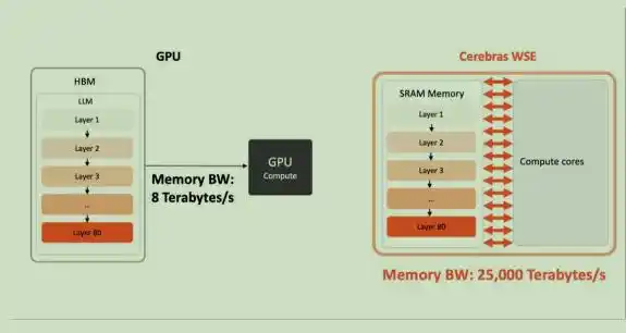
大模型推理的瓶颈不再仅仅是计算,而是数据搬运——模型权重、中间激活值和KV Cache需要在片外DRAM(如HBM)和GPU之间频繁交互,模型越大,数据搬移的能耗与延迟越高,最终远超计算本身的能耗,从而形成了内存墙。
英伟达GPU凭借CUDA和NVLink构筑了坚固堡垒,但仍然避免不了带宽瓶颈引发的GPU空转。
国内大模型公司智谱做了一个很简单的实验:一个512卡的推理集群,GPU不变、模型不变、代码不变,只把网络带宽上限从200GB/S换成400GGB/S,推理吞吐直接涨了10%,首token输出时延降了19%——道理很简单,只要把路拓宽,车就能跑得更快。
然而,以Cerebras为代表的非GPU架构,似乎正在内存墙上撕开一道口子。
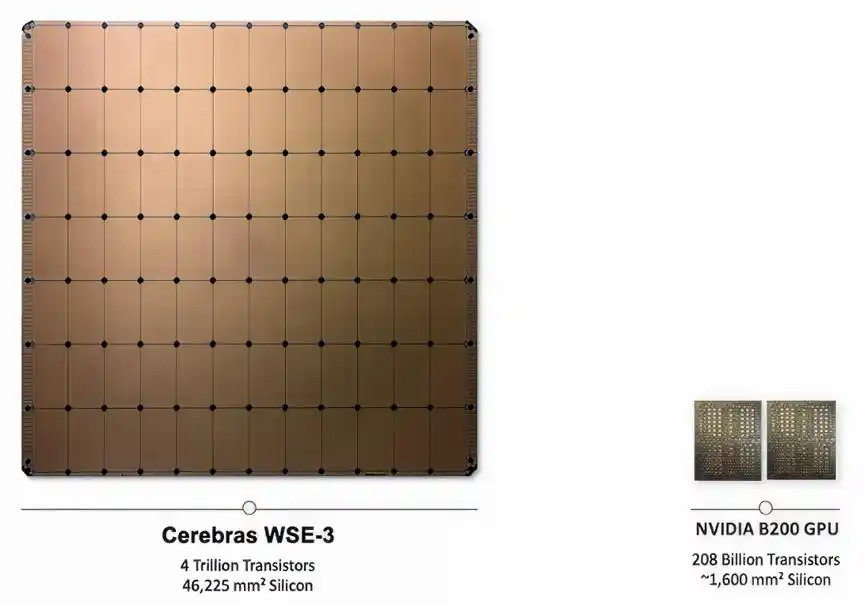
Cerebras WSE-3 芯片与英伟达B200 GPU 尺寸对比
Cerebras的本质:一台基于SRAM的近存计算机器
Cerebras Systems由 Andrew Feldman 等人在硅谷创立,早期的创始团队悉数来自一家叫SeaMicro的低功耗微服务器,这家公司后来被AMD收购,随后:
2015年,创始团队确立“晶圆级计算”路线;
2016年,完成注册、A轮融资,进入隐身研发阶段;
2019年,发布首款产品WSE-1 芯片和CS-1系统,基于台积电16nm工艺;
2021年,发布第二代产品,基于台积电7nm工艺;
2024年,发布第三代产品(WSE-3 / CS-3),基于台积电5nm工艺,芯片和系统均在美国完成制造,是地道的纯美国制造的芯片系统。
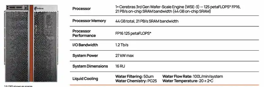
CS-3系统配置,包含1颗 WSE-3芯片
Cerebras的晶圆级引擎(Wafer-Scale Engine, WSE)架构哲学,简单粗暴却直击痛点:用物理空间的极致放大,换取对数据搬运延迟的极致压缩。
普通芯片是把一片晶圆切成很多小芯片,比如英伟达GPU就是这种思路。 Cerebras反过来:不切,直接把几乎整片晶圆做成一颗超大芯片,叫 Wafer-Scale Engine,WSE。
传统芯片是将一整块300mm直径晶圆,切割成数百个小芯片而形成;而Cerebras选择保留整片晶圆,直接作为整个芯片。最新的WSE-3拥有4万亿晶体管、90万个AI核心,每个核心配备48KB本地SRAM,从而让整个芯片的的片上SRAM达到44GB,提供21PB/秒的片上内存带宽(on‐chip memory bandwidth)和214Pb/秒的网络带宽(fabric bandwidth),这是传统HBM带宽的数千倍。
Cerebras WSE的内存带宽是英伟达B200封装芯片的2625倍,打破了大模型推理场景下的内存带宽瓶颈。
在Cerebras的架构中,模型权重从来都不会存在SRAM上,而是在片外存储MemoryX上,并逐层向大芯片上转移。实现方式是将神经网络模型的权重存储与计算单元相互分离。
所有模型权重均外置存放于内存扩展模块MemoryX中,网络每一层计算所需的权重,会按需逐层传输至CS-3系统。权重存储在MEMORY X的DRAM与闪存内,并以满带宽速率向CS-3系统传输。这些权重不会存入CS-3系统,就连临时缓存也不会留存,CS-3依靠核心底层的数据流机制完成运算。
Cerebras凭借晶圆级架构,在受限于内存带宽的LLM推理中,展现出降维打击般的壁垒。逐Token生成时,权重按层从片外MemoryX流式传输至CS-3,跑不同的模型,token速率是英伟达B200的1.5 - 5倍。
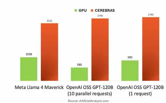
英伟达DGX B200 GPU versus Cerebras CS-3芯片,跑不同大模型的Token速率比较
其优势核心在于:CS-3的44GB片上SRAM提供21 PB/s(B200的2625倍)超高带宽与214 Pb/s互联,使权重流传输摆脱HBM接口限制。故在TTFT(Time To First Token,从请求发出到模型返回第一个token 的时间)、长上下文以及智能体工作负载上,表现尤为突出。
虽然权重外置于MemoryX按需逐层加载且不在片上缓存,CS-3依靠核心数据流机制在SRAM完成全FP16精度无损运算;凭借线性性能扩展,其在多用户并发推理下亦释放出惊人的总吞吐。
除了带宽,还有功耗的优势。近期,中际旭创董事长刘圣演讲中也提到,客户对于光模块的要求是1 pJ/bit,而当前是10 pJ/bit。在Cerebras芯片中,互联的功耗只有0.15 pJ/bit, 而当前GPU的互联功耗是10 pJ/bit。
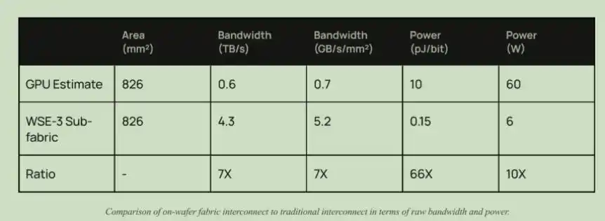
Cerebras互联与GPU互联架构的带宽和功耗对比
由此可见,如果Cerebras的晶圆级大芯片架构成为AI推理甚至训练的主流,也许将会对传统光模块和CPO(共封装光学)的出货量产生显著的抑制和结构性改变。核心逻辑在于:光模块和CPO的高需求,本质上是为了解决GPU集群中“芯片间互联”和“节点间互联”的带宽瓶颈;而Cerebras的架构恰恰是通过“消除分布式互联”来解决问题的。
反直觉:晶圆级大芯片的“真假”硬伤
芯片的核心永远在于Trade Off(取舍之道)。Cerebras为了片上SRAM的极致带宽,也带来一些问题。
良率低?
恰恰相反,单个AI核心尺寸减至0.05平方毫米(H100 单个运算核心尺寸的1%),因此良率反而更高。通过片上的路由,可关停和绕过有缺陷的核心,从而使得与传统多核处理器相比,缺陷容忍度提升了100倍。其实整个芯片有100万个AI核心,但是考虑了良率,对外声称是90万个AI核心。
只擅长推理,不擅长训练?
在Cerebras成立的数年之内,训练是主流课题,因此公司始终围绕着训练做了大量工作,只是推理需求火爆后,大家发现其在推理方面的优势更明显。
实际上简化的分布计算,也带来了代码复杂度降低、通信开销降低的一系列优势。
在4000块GPU上训练一个1750亿参数的模型,通常需要大约2万行分布式训练代码。
Cerebras 实现了565行代码的等效训练——整个模型可安装在晶圆上,且不需处理数据并行复杂性。
SRAM缩放已死,核心优势面临物理天花板。
第三代产品基于台积电5nm,其SRAM容量仅仅比基于台积电7nm的第二代产品增加了10%,在5nm之后,SRAM单元面积几乎不再随制程进步而缩小。
这意味着Cerebras无法再像过去那样,通过升级台积电制程(如从5nm走向3nm)来显著增加其核心优势(SRAM容量)。
受限于晶圆尺寸、散热能力及制造成本,片上SRAM等存储资源难以与计算核心同步线性扩展,资源配比遭遇瓶颈。这几乎堵死了其进化之路。
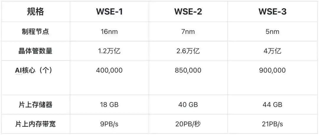
Cerebras 三代产品技术规格
散热、工艺与生态的三重炼狱。
整片晶圆集中发热,热流密度较高,必须依赖定制机房和专用液冷系统,此外,生态通用性意味着客户必须适应其定制化的软件栈,与现有CUDA等通用编程框架的兼容性弱,软件移植与适配成本高昂。
片外带宽低,成为扩展“孤岛”。
由于晶圆级物理设计的限制,WSE边缘能够引出的I/O引脚数量极其有限,导致其I/O带宽仅为150GB/s。这与英伟达NVLink动辄1.8TB/s的双向带宽相比,犹如蜗牛。这意味着WSE极难向外高速扩展。尽管Cerebras的SwarmX互联在多系统组合上做得尚可,但在需要多芯片高速互联的超大模型面前,极低的片外带宽成为了结构性的物理枷锁。
路线之争:大厂自研,Cerebras的窗口期还剩多久?
大厂解决“推理需要更高带宽+更低延迟”的方法,不止wafer-scale一条路,他们正在通过三条并行路径,对初创公司的技术红利进行围剿。
1 自研 ASIC芯片
Google TPU v8已经分裂为training-specific和inference-specific两个版本;AWS Trainium 4在路上;Microsoft Maia已在Azure内部使用,基于台积电 3nm 工艺构建,原生 FP8/FP4 张量核心,重新设计的内存系统,配备 216GB HBM3e,272MB 片上SRAM;甚至连Anthropic都开始评估自研inference chip。
这条路径的概率极高,它将直接导致“第三方inference采购”在2028年的TAM(总可达市场),上限被压缩10%到25%。
2 标准Packaging路线的工艺通用化
这是对Cerebras最直接的降维打击。
TSMC的SoW(System-on-Wafer)已经向客户广泛开放,CoWoS 9.5x interposer也将在2027年上线。
这两个产品做的事——把多颗die在wafer级别stitching——本质上就是把Cerebras的物理工艺通用化、平民化。
英伟达的Vera Rubin将在2026下半年进入这个生态。
Cerebras自家做的cross-reticle stitching虽是独占,但独占的窗口期最长只有2到3年,到2027 - 2028年之后,其工艺壁垒将被台积电的先进封装稀释。
3 光互联/光计算的突围
电子芯片的互联与内存墙已至极限,光子的高带宽、低延迟、零串扰是终极解法。
以Lumentum为代表的光学路线正在崛起。Wafer-scale的最大优势就是片上计算,但模型必然越来越大,wafer scale往上的高速互联是刚需。
随着CPO(共封装光学)和Optical Interconnects的成熟,未来我们极有可能看到光I/O直接引入WSE晶圆,打破电互联枷锁;而英伟达也可能通过收购LPU(如Groq)等具备特定架构优势的公司,结合光互联,开发兼容现有NV超节点软件的晶圆级系统。
悬崖上的狂奔:Cerebras的商业与交付
Cerebras目前正面临一场由巨额订单倒逼的悬崖式狂奔。
与OpenAI等头部大客户的交易,迫使Cerebras从一家芯片公司转型为新型云服务商。它不再只是卖硬件,而是需要在短期内锁定并建设海量的数据中心电力和设施。
根据合同要求,Cerebras需要在2026 - 2028年每年交付250MW的数据中心容量。然而,晶圆级系统对机房的要求极高,无法直接塞进传统的风冷IDC。目前,Cerebras在数据中心容量的筹备上进度已经明显落后于合同要求。
从流片到建厂,从电力审批到冷却系统部署,这是一个重资产、长周期的泥潭。
尾声:向左还是向右?
回到最初的命题,当推理算力拐点已至,算力架构的核心永远在于取舍。
没有绝对的对错,只有在最重要负载下的相对最优解。负载其实已经在变。
Cerebras向左,选择了极致的物理优化,用整片晶圆和海量SRAM换取单任务下的极致低延迟,这对首token延迟极度敏感的场景下是无敌的。
英伟达向右,选择了保持通用性,用HBM + NVLink + 超大集群吞吐,应对负载的千变万化,以不变应万变。
风起云涌,前路未卜。正是这种技术与商业的双重不确定性,才孕育着颠覆的可能。在通往AGI的算力洪流中,现在下定论还为时尚早——因为不确定,才有机会。
本文来自微信公众号“大蒜粒机研所”,作者:霹雳游侠