From Sand to Chips: Hefei's Semiconductor Alchemy

marsbitPublished on 2026-07-28Last updated on 2026-07-28

Abstract

From Sand to Chips: Hefei's Semiconductor "Alchemy" On July 27, 2026, a memory chip maker from Hefei made history by surpassing the market capitalization of Industrial and Commercial Bank of China on its Shanghai Stock Exchange debut. This marks the culmination of Hefei's two-decade industrial transformation, often summarized in three strategic leaps: "Screen, Chip, Vehicle." The journey began in 2008 with a bold investment in BOE, establishing China's first 6th-generation LCD panel line. The second leap was the "Project 506" in 2016, which gave birth to ChangXin Memory Technologies (CXMT). With initial backing of 14.4 billion RMB from Hefei's state-owned investment platform, CXMT aimed to break into the global DRAM market, then over 95% controlled by three overseas giants. CXMT achieved a breakthrough in 2019 by producing China's first 8GB DDR4 DRAM chip, employing "generational leapfrog" R&D to catch up. After years of significant losses, the company turned profitable in 2025. A dramatic surge followed in 2026, driven by AI-driven demand and full capacity utilization, propelling CXMT to become the world's fourth-largest DRAM manufacturer. CXMT's success is not isolated. It anchors a dense, localized semiconductor ecosystem in Hefei. Within its vicinity are numerous supporting companies for equipment, materials, and packaging & testing. This cluster has fueled the regional economy, with Hefei's integrated circuit industry output growing over sevenfold between 2016 and 20...

On July 27, 2026, when the gong sounded at the Shanghai Stock Exchange, the history of China's capital markets was rewritten.

A company making memory chips closed its first trading day with a market capitalization of 3.28 trillion yuan, surpassing Industrial and Commercial Bank of China (ICBC).

This was not a financial stock, not an energy giant, not an internet platform, but a manufacturing enterprise that extracts silicon from sand, etches circuits onto silicon wafers, and turns those circuits into memory chips.

Its headquarters are not in Shenzhen, not in Shanghai, not in Beijing.

It's in Hefei.

How did an inland city, mocked twenty years ago as "China's largest county seat," hatch the world's fourth-largest memory chip manufacturer? How did a company founded in 2016 surpass ICBC in market value just ten years later?

The more crucial question is: With such a large enterprise landing in Hefei, what has grown around it? How did sand transform step by step into chips? And who are the companies that became its neighbors?

Project 506

On May 6, 2016, a codename was born.

Zhu Yiming ("Lao Zhu"), then Chairman and General Manager of GigaDevice, sat down with Hefei city leaders to discuss building a DRAM project. This day later became known as "506," and the project was named "Project 506."

The backdrop was alarming: Samsung Electronics, SK Hynix, and Micron controlled over 95% of the global DRAM market, while mainland China had almost no large-scale DRAM manufacturing capability. The core technology in every memory stick inside every mobile phone, computer, and server worldwide was held by these three overseas giants.

Lao Zhu wanted to do this. But he couldn't do it alone. DRAM is a capital-intensive industry; a single 12-inch wafer production line requires investment of tens of billions, has extremely high technical barriers, and yield ramp-up cycles are measured in years.

Hefei made the decision.

In 2017, GigaDevice and Hefei Industry Investment formally signed a cooperation agreement. The initial project budget was 18 billion yuan, with GigaDevice contributing 3.6 billion yuan (20%) and Hefei Industry Investment contributing 14.4 billion yuan (80%).

And this was just Phase One. The total investment for the entire ChangXin Memory (CXMT) dynamic random-access memory chip base reached 150 billion yuan, making it Anhui's largest single industrial investment project at the time.

Why would Hefei invest so heavily?

The answer lies in a plan from three years earlier. In 2013, Hefei issued the "Integrated Circuit Industry Development Plan (2013–2020)," proposing for the first time to build a "Chinese Silicon Valley." CXMT was the most critical piece on this chessboard.

China's First Domestically Produced DRAM Chip

In September 2019, the CXMT 12-inch wafer fab began production.

What came off the production line that day was an 8GB DDR4 memory chip—a breakthrough from 0 to 1 for mainstream domestic DRAM chips.

From the project launch in May 2016 to the first product off the line in September 2019: three years and four months. During this period, CXMT completed "skip-generation R&D" from its first- to fourth-generation process technology platforms, achieving product coverage and iteration from DDR4 and LPDDR4X to DDR5 and LPDDR5/5X.

What does "skip-generation R&D" mean? Samsung and Hynix spent twenty years, generation by generation, progressing from DDR1 to DDR5, with three to five years between each generation. CXMT didn't have a twenty-year window; it had to skip intermediate generations and directly catch up to mainstream manufacturing processes.

After the first DDR4 chip came off the line in 2019, CXMT's products gradually iterated to DDR5 and LPDDR5/5X, which are the mainstream configurations for global AI servers and flagship smartphones today.

But technological breakthroughs don't equal profitability. The following years were far more difficult for CXMT than outsiders imagined.

From a 16.3 Billion Loss to Quarterly Profits of 24.7 Billion

The financial data of ChangXin Memory Technology (CXMT's listed entity) is like a roller coaster.

2023: Revenue of 9.087 billion yuan, net profit attributable to shareholders: a loss of 16.340 billion yuan.

2024: Net profit attributable to shareholders: a loss of 7.145 billion yuan.

But in 2025, the plot reversed. Annual revenue reached 61.799 billion yuan, a year-on-year increase of 155.62%; net profit attributable to shareholders was 1.875 billion yuan, achieving profitability for the first time. Non-GAAP net profit was 5.316 billion yuan, and gross profit margin from main business rose to 41.02%.

By the first quarter of 2026, the data exploded: Revenue of 50.8 billion yuan, up 719.13% year-on-year; net profit attributable to shareholders of 24.762 billion yuan, up 1688.30% year-on-year.

A single quarter's profit of 24.7 billion yuan covered the combined losses of 23.5 billion yuan from 2023 and 2024, with money left over.

The company forecast revenue for the first half of 2026 to be between 110 and 120 billion yuan, with net profit attributable to shareholders between 50 and 57 billion yuan. At this rate, annual net profit could exceed 100 billion yuan.

Why the explosion? Two reasons: First, AI is driving global DRAM supply shortages, with prices continuously rising. Second, CXMT's own capacity and yield ramp-up reached target levels, with capacity utilization reaching 95.73% in 2025.

Changes in global market share are even more telling. According to Counterpoint data, CXMT's global DRAM market share was 3% in Q1 2025, rising to 4% in Q2, 6% in Q3, and surging to 8% in Q4. More than doubling in a year. By Q1 2026, it stabilized at 8%, ranking fourth globally, following Samsung, SK Hynix, and Micron.

But CXMT's explosion is not a one-man show.

The Supporting Ecosystem from Sand to Chip

A DRAM chip goes from nothing to something through this process:

Silicon purification - Crystal pulling into silicon ingots - Slicing into silicon wafers - Photolithography - Etching - Thin-film deposition - Chemical mechanical polishing (CMP) - Cleaning - Dicing - Packaging - Testing - Finished product.

Each step requires specialized companies and equipment. CXMT handles the midstream wafer manufacturing, but without upstream equipment, materials, and downstream packaging and testing support, it would be an isolated island.

Hefei's industrial ecosystem precisely connects these islands into a continent.

In July 2026, a Securities Times reporter visited CXMT's core factory area and discovered an astonishing phenomenon: surrounding CXMT's facility were densely packed semiconductor equipment, materials, and testing companies, all providing nearby support.

Hefei Powertech Semiconductor, just across the road from CXMT, primarily provides packaging and testing services for CXMT's memory chips. With an investment of about 10 billion yuan, construction started in March 2021, formal production began in December of the same year. In May 2026, the company stated its Hefei packaging and testing plant was currently operating at full capacity and actively expanding based on customer demand.

The Xinqiao Integrated Circuit Technology Park is also adjacent to CXMT. This 172-acre park was planned simultaneously with CXMT's "Project 506" in 2016, opened in 2019, and has gathered over 20 semiconductor upstream and downstream enterprises.

Who's in the park?

Equipment: Hefei Naura Microelectronics Equipment Co., Ltd. (a subsidiary of Naura), providing key equipment like etching and thin-film deposition; Hefei Jingzhida Integrated Circuit Technology Co., Ltd. (under Jingzhida); ACM Research (Shanghai) has offices here; Kaiyue Semiconductor independently develops coater/developers, having upgraded from refurbishing imported second-hand equipment to independent innovation; Wanweikelin provides semiconductor equipment.

Packaging & Testing: Xinfeng Technology represents semiconductor packaging and testing projects.

Materials & Components: Hemeng Precision, Sanyue Vacuum provide semiconductor components and materials.

Supporting Services: Qichuan Technology, Huahai Qingke provide semiconductor supporting services.

Beyond this, across Hefei's broader landscape, there are even more supporting companies. Among upstream equipment suppliers, Naura, AMEC, Piotech, and Huahai Qingke already supply key equipment like etching, thin-film deposition, and CMP to CXMT.

In high-end materials: Yoke Technology supplies precursor products; Guanggang Gas, Jinhong Gas provide electronic specialty gases;彤程新材 (Red Avenue New Materials) and晶瑞电材 (Jingrui Electric Materials) have entered the photoresist supply chain.

The downstream client roster is equally impressive: Alibaba Cloud, Tencent, ByteDance, Lenovo, Xiaomi, Honor, OPPO.

In this IPO's strategic placement, semiconductor industry chain companies like AMEC and Piotech, as well as downstream enterprises like Xiaomi, TCL, Kuaishou, NIO, and Alibaba Cloud, all received allocated shares, creating deep ties through equity investment and business synergy.

According to incomplete statistics, CXMT involves over 30 A-share listed companies. Hefei's integrated circuit industry output value grew from about 18 billion yuan in 2016 to 151.4 billion yuan in 2025, an increase of over 7 times, with a CAGR exceeding 26%. The city now has over 400 integrated circuit enterprises.

This isn't one company; it's an entire industrial chain.

One Factory Ignites a Whole Street

CXMT's industrial ripple effect even extends to roadside snack stalls.

The CXMT factory area is located near Hefei Xinqiao Airport in the Changgang community. A Securities Times reporter's visit found the most bustling area around the factory is along Shuofang Road, jokingly called the "Changgang CBD" by locals.

Both sides of Shuofang Road are densely packed with restaurants, supermarkets, hotels, pharmacies, hair salons, entertainment venues, etc., some operating 24/7. The night market stays open until 2-3 AM. A skewer stall owner said at least half the business comes from CXMT employees or clients.

Even more exaggerated are the hotels. A Hampton by Hilton on Shuofang Road with over 170 rooms is basically fully booked on weekdays, with over 80% of guests traveling on CXMT business. Some long-term, high-frequency business clients directly book rooms for extended stays.

Frequent travel by CXMT's upstream and downstream clients creates severe accommodation shortages; not being able to book a room on weekdays is the norm.

A supplier's on-site personnel told the reporter he rented an apartment nearby, brought his wife and child, and had been stationed there for over half a year. At 10 PM, delivery vehicles were still coming and going on the Xinhua Avenue freight route. A truck driver from Beijing said one truckload of equipment was worth hundreds of millions of yuan.

South of the factory, the second-phase project of the 12-inch memory wafer manufacturing base is under construction through the night, with tower cranes operating and machines rumbling. The production lines run 24/7 without stopping.

The busyness of one factory area reflects the vibrancy of an entire industrial chain.

Hefei's Three Leaps

CXMT was not Hefei's first big gamble, nor its last.

Hefei's industrial rise has been summarized by outsiders as three leaps: Screen, Chip, Vehicle.

First Leap: Screen. In 2008, Hefei postponed subway construction, allocated about one-third of its local fiscal revenue to introduce BOE, which was losing over 1 billion yuan at the time, to build China's first 6th-generation LCD panel line. BOE later became China's panel leader, building multiple production lines in Hefei, driving the Xinzhan High-tech Zone's new display industry output value to exceed 120 billion yuan.

Hefei surpassed Shenzhen to top the list of China's top ten cities for new display industry.

Second Leap: Chip. Launching "Project 506" in 2016, CXMT landed. Hefei Industry Investment contributed 14.4 billion yuan, an 80% stake. Total investment of 150 billion yuan made it Anhui's largest single industrial investment project then.

Third Leap: Vehicle. In 2020, Hefei Construction Investment joined forces with three state-owned capital platforms to raise 7 billion yuan and introduce the nearly bankrupt NIO. After NIO China's headquarters settled in Hefei,整车龙头 (vehicle leaders) like BYD, Volkswagen, and supporting enterprises followed. In 2025, Hefei's new energy vehicle output reached 1.376 million units, ranking first among Chinese cities for two consecutive years, with industrial cluster revenue exceeding 600 billion yuan.

Three leaps pieced together Hefei's "Chip, Screen, Auto, Home Appliance, and AI" industrial skeleton, with chips, displays, automobiles, home appliances, and artificial intelligence supporting each other.

In 2025, Hefei's GDP reached 1.42 trillion yuan, ranking 18th nationally. Its GDP growth rate topped the list among China's top 20 cities by economic size in both 2024 and 2025. In Q1 2026, GDP was 322.96 billion yuan, a year-on-year increase of 6.8%, the highest growth rate among 29 cities with trillion-yuan GDP.

From a GDP of only 58.97 billion yuan in 2005, mocked as "China's largest county seat," to today's "Double Ten-Thousand City" (trillion-yuan GDP, ten-million population), Hefei took twenty years, advancing 70 places in ranking.

Is Hefei Suitable for Employment and Living?

After CXMT's listing, a practical question was repeatedly raised: Is Hefei a city suitable for ordinary people to work and live in?

First, employment.

Hefei plans to create 200,000 job positions in key industry sectors in 2026. Since 2023, it holds an annual "Hefei Invites You, 200,000 Positions for You to Choose" series of job fairs, facilitating 278,000 employment intentions over three years. It attracts over 350,000 university graduates annually.

Regarding salaries, semiconductor technicians who moved from Shanghai to Hefei reported salaries decreased by only about 10%, but job stability is stronger, with far less risk of mid-career unemployment compared to first-tier cities.

Now, cost of living.

In June 2026, the average price for new homes in Hefei was about 17,900 yuan/m2. By district: Zhengwu District averaged 31,767 yuan/m2, the city's highest; Binhu District 24,405 yuan/m2; High-tech Zone 24,373 yuan/m2; Economic Development Zone 23,678 yuan/m2; Baohe District 23,084 yuan/m2. Outlying areas ranged from 7,000-8,000 yuan/m2.

Compared to the Yangtze River Delta: Nanjing's average new home price is around 30,000+; Hangzhou 35,000+. Hefei is only half to two-thirds of those. The house price-to-income ratio is about 10.2, not low, but far lower than first-tier cities' 15-20.

For commute, the average commute within Hefei's urban area is 38 minutes, nearly a quarter-hour less than the 45-50 minutes in Beijing, Shanghai, Guangzhou, and Shenzhen. A resident who returned from Beijing said: "My income in Hefei is similar to what it was in Beijing, but my happiness is much higher. No need to squeeze onto subways, it's 20-30 minutes to get anywhere, and things are cheaper."

Education and healthcare are also upgrading. In 2026, Hefei plans to newly build, renovate, or expand 43 primary/secondary schools and kindergartens, adding 38,000 new student places, aiming to increase the普通高中 (普通高中) admission rate to 85%. The Hefei Public Health Clinical Medical Center will open for operation, 5 smart hospitals will be completed, 5 national regional medical centers will be enhanced, and 20 new名医工作室 (renowned doctor studios) will be established.

Consumer-wise: Sam's Club's first Anhui store opened in Hefei in April 2025, with over 50,000 member registrations on opening day. Aldi is即将落地 (soon to land).高端户外品牌 (High-end outdoor brands) like Arc'teryx and Salomon have achieved布局密度 (distribution density) in Hefei comparable to Suzhou and Wuxi. Non-standard commercial streets like新粮仓 (New Granary) and瑶海天地 (Yaohai Tiandi) are called "Hefei's新天地 (Xintiandi)."

Annually, about 30% of University of Science and Technology of China (USTC) graduates choose to stay in Hefei to start businesses or work. Among Hefei's STAR Market-listed companies, USTC-affiliated enterprises account for over 30%; among unicorn companies, USTC-affiliated enterprises account for over 40%.

...

From sand to chips, from county seat to trillion-yuan city, this road took Hefei twenty years.

Turning sand into chips requires over a thousand processes. Turning a county seat into a trillion-yuan city requires twenty years of staying the course.

This requires extreme long-termism and the ability to endure solitude.

This article is from the WeChat public account "Washu66" (ID: washu66), author: Washu

Trending Cryptos

Related Questions

QWhat was the project codename for the DRAM initiative established by GigaDevice and Hefei in 2016, and what is its significance?

AThe project codename was '506 Engineering', derived from the date of May 6, 2016, when the discussions were held. It is significant as it marked the launch of Changxin Technology's DRAM project, a massive investment by Hefei to build domestic DRAM manufacturing capabilities and break the monopoly of three overseas giants (Samsung, SK Hynix, Micron) that controlled over 95% of the global market at the time.

QAccording to the article, what were the key factors behind Changxin Technology's dramatic financial turnaround from heavy losses to massive profits between 2023-2026?

AThe key factors were: 1. AI-driven global demand leading to a supply shortage and rising prices for DRAM chips. 2. Changxin's own capacity and yield rates reaching optimal levels, with capacity utilization hitting 95.73% in 2025. This combination allowed the company to move from significant annual losses to achieving a quarterly net profit of 247.62 billion yuan in Q1 2026.

QHow did the article describe the industrial ecosystem supporting Changxin Technology in Hefei?

AThe article describes a dense, localized semiconductor ecosystem. Changxin's core manufacturing is supported by numerous nearby companies providing upstream equipment (etching, deposition, CMP), materials (specialty gases, photoresists), and downstream services like packaging and testing (e.g., Hefei沛顿存储). The Xinqiao Integrated Circuit Science Park, planned alongside Changxin, hosts over 20 such companies. This cluster transforms Hefei from having an isolated factory into a complete, interconnected industrial chain.

QWhat are the 'three leaps' in Hefei's industrial development strategy as summarized in the article?

AHefei's industrial strategy is summarized as three major leaps: 1. The 'Screen' leap: Investing in BOE in 2008 to establish a liquid crystal panel industry. 2. The 'Chip' leap: Launching the '506 Engineering' with Changxin in 2016 to build a semiconductor memory industry. 3. The 'Vehicle' leap: Investing in NIO in 2020 to cultivate a new energy vehicle industry. These leaps collectively form the city's 'Core, Screen, Vehicle, and Convergence' industrial framework.

QBased on the article, what are some arguments presented for Hefei being a suitable city for employment and living, especially for professionals?

AArguments for Hefei's suitability include: 1. Employment: Strong job creation (200,000 planned positions in 2026), high graduate retention, and competitive salaries for tech professionals (e.g., only ~10% less than Shanghai with greater job stability). 2. Living Costs: Lower housing prices (average ~17,900 RMB/m²) compared to major eastern cities like Nanjing and Hangzhou. 3. Convenience: Shorter average commute (38 minutes) than first-tier cities. 4. Amenities: Improving education, healthcare, and consumer retail options, including international brands. Overall, it offers a high quality of life with lower pressure than mega-cities.

Related Reads

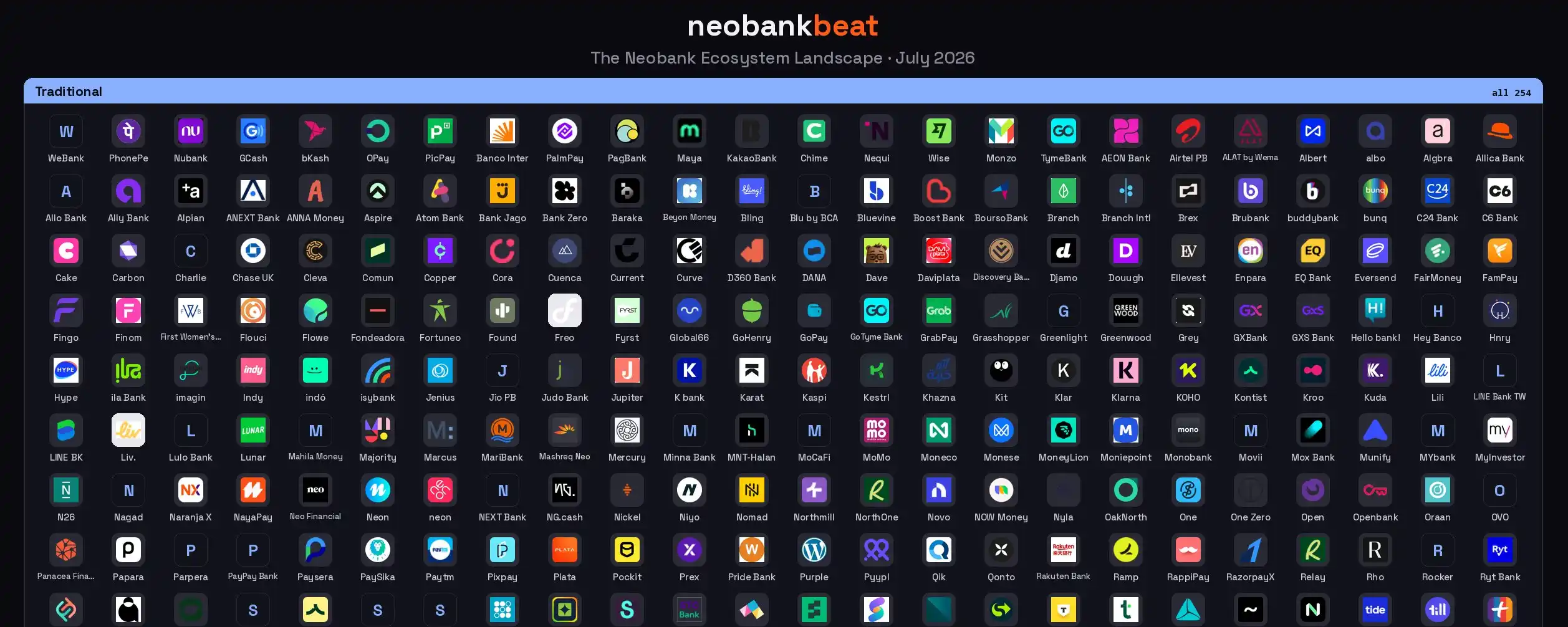
The Truth Behind Digital Banking: The Fragile Ecosystem Supporting 1.46 Billion Users

The article "The Truth About Digital Banks: The Fragile Ecosystem Behind 1.46 Billion Users" provides a data-driven analysis of the digital banking sector based on a verified list of 368 active neobanks as of July 2026. While these platforms collectively serve 1.46 billion users, with Asia (817 million users) and institutions like WeBank and Nubank dominating the landscape, the sector faces significant structural vulnerabilities. A key finding is that only 127 of the 368 neobanks hold full banking licenses. The majority operate atop third-party infrastructure providers like Banking-as-a-Service (BaaS) platforms, creating systemic risk where the failure of a single provider, as seen in past cases like Wirecard and Synapse, can jeopardize multiple consumer brands. Furthermore, the industry experiences a steady, quiet stream of failures, mergers, and shutdowns that often go unreported. The analysis also examines the adoption of artificial intelligence (AI), finding only 67 platforms (18%) have deployed AI at scale, with many innovators based in emerging markets like Nigeria and the Philippines. The infrastructure layer is highly concentrated, with 106 providers supporting the entire ecosystem of 368 consumer-facing brands. The article concludes with three predictions: the unlicensed gap will close through acquisitions or exits; an AI credit model is likely to fail in the next economic downturn; and a nascent but significant trend is the emergence of financial services designed for AI agents rather than humans.

marsbit16m ago

The Truth Behind Digital Banking: The Fragile Ecosystem Supporting 1.46 Billion Users

marsbit16m ago

Digital Asset Trading Platform Uphold Cuts 17% of Global Workforce Amid 'Crypto Winter'

Cryptocurrency trading platform Uphold has laid off approximately 17% of its global workforce, affecting 85 full-time employees and contractors. The cuts are part of a strategic shift to reallocate resources towards its rapidly growing corporate services business, as retail cryptocurrency trading activity has declined amid the ongoing market downturn. CEO Simon McLaughlin stated the company is restructuring after years of significant growth and remains confident in the long-term prospects of digital assets and blockchain technology. Founded in 2015, Uphold offers trading and custody services for cryptocurrencies, fiat, stocks, and precious metals. It has recently expanded to provide infrastructure for banks, fintech firms, and broker-dealers to integrate crypto services. The layoffs occur against a backdrop of a prolonged crypto market slump, with total market capitalization falling to around $2.1 trillion by Q2 2024. Factors include weakened trading volumes, reduced retail participation, interest rate hikes, geopolitical uncertainty, and net outflows from U.S. spot Bitcoin ETFs. Uphold clarified it is not shutting down its UK operations or any international offices. The company highlighted strong growth in its corporate platform and announced plans to evolve its consumer app into a broader blockchain-based financial assistant by 2026, offering U.S. stocks, tokenized securities, lending, credit cards, and DeFi yield opportunities.

cryptonews.ru16m ago

Digital Asset Trading Platform Uphold Cuts 17% of Global Workforce Amid 'Crypto Winter'

cryptonews.ru16m ago

Has the Crypto Utopia Collapsed? The Industry Reaches an Inflection Point After the Frenzy Subsides

Has the crypto utopia collapsed? The industry is at an inflection point as the hype fades. The prevailing view is that crypto has become an outlet for excess liquidity, with many participants leaving as financial returns have fallen short of past-decade expectations. The 2021 boom has been revealed as an illusion, placing the industry in the "trough of disillusionment" on Gartner's Hype Cycle. This forces a return to first principles: re-evaluating token value, securing DeFi protocols, and finding real-world applications. The core failure is a repetitive cycle of reflexive speculation, driven by the premature liquidity of tokens. The industry's incentives prioritized short-term gains over genuine innovation. While curiosity drives invention, recent DeFi hacks signal a need for engineering and iteration, including token models. The culture is shifting; the industry is no longer in its early stages. Positioned at a turning point on the technology adoption curve, crypto faces the immense challenge of rebuilding finance from scratch, a process of inevitable iteration and failure. Regarding crypto VC, claims of its death are overstated. The exceptional returns of 2016-2021 were an anomaly. The initial crypto-anarchist ethos has largely been co-opted by Wall Street and regulators. The utopian vision is over; the industry is being assimilated into the existing system, becoming a business. Current viable project categories include stablecoins, prediction markets, tokenized assets/RWA, perpetual contracts, and AI/agent integration. Crypto is converging with fintech, far from the envisioned DeFi revolution, and must find killer apps within regulatory boundaries. A reconciliation is possible: cryptocurrency may change value storage and transfer in subtle, imperceptible ways that integrate into existing systems, rather than through revolutionary fanfare. True creativity often emerges from adversity. There remains much to build for those driven by genuine curiosity.

marsbit30m ago

Has the Crypto Utopia Collapsed? The Industry Reaches an Inflection Point After the Frenzy Subsides

marsbit30m ago

Trading

Spot

Hot Articles

What is SONIC

Sonic: Pioneering the Future of Gaming in Web3 Introduction to Sonic In the ever-evolving landscape of Web3, the gaming industry stands out as one of the most dynamic and promising sectors. At the forefront of this revolution is Sonic, a project designed to amplify the gaming ecosystem on the Solana blockchain. Leveraging cutting-edge technology, Sonic aims to deliver an unparalleled gaming experience by efficiently processing millions of requests per second, ensuring that players enjoy seamless gameplay while maintaining low transaction costs. This article delves into the intricate details of Sonic, exploring its creators, funding sources, operational mechanics, and the timeline of significant events that have shaped its journey. What is Sonic? Sonic is an innovative layer-2 network that operates atop the Solana blockchain, specifically tailored to enhance the existing Solana gaming ecosystem. It accomplishes this through a customised, VM-agnostic game engine paired with a HyperGrid interpreter, facilitating sovereign game economies that roll up back to the Solana platform. The primary goals of Sonic include: Enhanced Gaming Experiences: Sonic is committed to offering lightning-fast on-chain gameplay, allowing players and developers to engage with games at previously unattainable speeds. Atomic Interoperability: This feature enables transactions to be executed within Sonic without the need to redeploy Solana programmes and accounts. This makes the process more efficient and directly benefits from Solana Layer1 services and liquidity. Seamless Deployment: Sonic allows developers to write for Ethereum Virtual Machine (EVM) based systems and execute them on Solana’s SVM infrastructure. This interoperability is crucial for attracting a broader range of dApps and decentralised applications to the platform. Support for Developers: By offering native composable gaming primitives and extensible data types - dining within the Entity-Component-System (ECS) framework - game creators can craft intricate business logic with ease. Overall, Sonic's unique approach not only caters to players but also provides an accessible and low-cost environment for developers to innovate and thrive. Creator of Sonic The information regarding the creator of Sonic is somewhat ambiguous. However, it is known that Sonic's SVM is owned by the company Mirror World. The absence of detailed information about the individuals behind Sonic reflects a common trend in several Web3 projects, where collective efforts and partnerships often overshadow individual contributions. Investors of Sonic Sonic has garnered considerable attention and support from various investors within the crypto and gaming sectors. Notably, the project raised an impressive $12 million during its Series A funding round. The round was led by BITKRAFT Ventures, with other notable investors including Galaxy, Okx Ventures, Interactive, Big Brain Holdings, and Mirana. This financial backing signifies the confidence that investment foundations have in Sonic’s potential to revolutionise the Web3 gaming landscape, further validating its innovative approaches and technologies. How Does Sonic Work? Sonic utilises the HyperGrid framework, a sophisticated parallel processing mechanism that enhances its scalability and customisability. Here are the core features that set Sonic apart: Lightning Speed at Low Costs: Sonic offers one of the fastest on-chain gaming experiences compared to other Layer-1 solutions, powered by the scalability of Solana’s virtual machine (SVM). Atomic Interoperability: Sonic enables transaction execution without redeployment of Solana programmes and accounts, effectively streamlining the interaction between users and the blockchain. EVM Compatibility: Developers can effortlessly migrate decentralised applications from EVM chains to the Solana environment using Sonic’s HyperGrid interpreter, increasing the accessibility and integration of various dApps. Ecosystem Support for Developers: By exposing native composable gaming primitives, Sonic facilitates a sandbox-like environment where developers can experiment and implement business logic, greatly enhancing the overall development experience. Monetisation Infrastructure: Sonic natively supports growth and monetisation efforts, providing frameworks for traffic generation, payments, and settlements, thereby ensuring that gaming projects are not only viable but also sustainable financially. Timeline of Sonic The evolution of Sonic has been marked by several key milestones. Below is a brief timeline highlighting critical events in the project's history: 2022: The Sonic cryptocurrency was officially launched, marking the beginning of its journey in the Web3 gaming arena. 2024: June: Sonic SVM successfully raised $12 million in a Series A funding round. This investment allowed Sonic to further develop its platform and expand its offerings. August: The launch of the Sonic Odyssey testnet provided users with the first opportunity to engage with the platform, offering interactive activities such as collecting rings—a nod to gaming nostalgia. October: SonicX, an innovative crypto game integrated with Solana, made its debut on TikTok, capturing the attention of over 120,000 users within a short span. This integration illustrated Sonic’s commitment to reaching a broader, global audience and showcased the potential of blockchain gaming. Key Points Sonic SVM is a revolutionary layer-2 network on Solana explicitly designed to enhance the GameFi landscape, demonstrating great potential for future development. HyperGrid Framework empowers Sonic by introducing horizontal scaling capabilities, ensuring that the network can handle the demands of Web3 gaming. Integration with Social Platforms: The successful launch of SonicX on TikTok displays Sonic’s strategy to leverage social media platforms to engage users, exponentially increasing the exposure and reach of its projects. Investment Confidence: The substantial funding from BITKRAFT Ventures, among others, emphasizes the robust backing Sonic has, paving the way for its ambitious future. In conclusion, Sonic encapsulates the essence of Web3 gaming innovation, striking a balance between cutting-edge technology, developer-centric tools, and community engagement. As the project continues to evolve, it is poised to redefine the gaming landscape, making it a notable entity for gamers and developers alike. As Sonic moves forward, it will undoubtedly attract greater interest and participation, solidifying its place within the broader narrative of blockchain gaming.

1.9k Total ViewsPublished 2024.04.04Updated 2024.12.03

What is SONIC

What is $S$

Understanding SPERO: A Comprehensive Overview Introduction to SPERO As the landscape of innovation continues to evolve, the emergence of web3 technologies and cryptocurrency projects plays a pivotal role in shaping the digital future. One project that has garnered attention in this dynamic field is SPERO, denoted as SPERO,$$s$. This article aims to gather and present detailed information about SPERO, to help enthusiasts and investors understand its foundations, objectives, and innovations within the web3 and crypto domains. What is SPERO,$$s$? SPERO,$$s$ is a unique project within the crypto space that seeks to leverage the principles of decentralisation and blockchain technology to create an ecosystem that promotes engagement, utility, and financial inclusion. The project is tailored to facilitate peer-to-peer interactions in new ways, providing users with innovative financial solutions and services. At its core, SPERO,$$s$ aims to empower individuals by providing tools and platforms that enhance user experience in the cryptocurrency space. This includes enabling more flexible transaction methods, fostering community-driven initiatives, and creating pathways for financial opportunities through decentralised applications (dApps). The underlying vision of SPERO,$$s$ revolves around inclusiveness, aiming to bridge gaps within traditional finance while harnessing the benefits of blockchain technology. Who is the Creator of SPERO,$$s$? The identity of the creator of SPERO,$$s$ remains somewhat obscure, as there are limited publicly available resources providing detailed background information on its founder(s). This lack of transparency can stem from the project's commitment to decentralisation—an ethos that many web3 projects share, prioritising collective contributions over individual recognition. By centring discussions around the community and its collective goals, SPERO,$$s$ embodies the essence of empowerment without singling out specific individuals. As such, understanding the ethos and mission of SPERO remains more important than identifying a singular creator. Who are the Investors of SPERO,$$s$? SPERO,$$s$ is supported by a diverse array of investors ranging from venture capitalists to angel investors dedicated to fostering innovation in the crypto sector. The focus of these investors generally aligns with SPERO's mission—prioritising projects that promise societal technological advancement, financial inclusivity, and decentralised governance. These investor foundations are typically interested in projects that not only offer innovative products but also contribute positively to the blockchain community and its ecosystems. The backing from these investors reinforces SPERO,$$s$ as a noteworthy contender in the rapidly evolving domain of crypto projects. How Does SPERO,$$s$ Work? SPERO,$$s$ employs a multi-faceted framework that distinguishes it from conventional cryptocurrency projects. Here are some of the key features that underline its uniqueness and innovation: Decentralised Governance: SPERO,$$s$ integrates decentralised governance models, empowering users to participate actively in decision-making processes regarding the project’s future. This approach fosters a sense of ownership and accountability among community members. Token Utility: SPERO,$$s$ utilises its own cryptocurrency token, designed to serve various functions within the ecosystem. These tokens enable transactions, rewards, and the facilitation of services offered on the platform, enhancing overall engagement and utility. Layered Architecture: The technical architecture of SPERO,$$s$ supports modularity and scalability, allowing for seamless integration of additional features and applications as the project evolves. This adaptability is paramount for sustaining relevance in the ever-changing crypto landscape. Community Engagement: The project emphasises community-driven initiatives, employing mechanisms that incentivise collaboration and feedback. By nurturing a strong community, SPERO,$$s$ can better address user needs and adapt to market trends. Focus on Inclusion: By offering low transaction fees and user-friendly interfaces, SPERO,$$s$ aims to attract a diverse user base, including individuals who may not previously have engaged in the crypto space. This commitment to inclusion aligns with its overarching mission of empowerment through accessibility. Timeline of SPERO,$$s$ Understanding a project's history provides crucial insights into its development trajectory and milestones. Below is a suggested timeline mapping significant events in the evolution of SPERO,$$s$: Conceptualisation and Ideation Phase: The initial ideas forming the basis of SPERO,$$s$ were conceived, aligning closely with the principles of decentralisation and community focus within the blockchain industry. Launch of Project Whitepaper: Following the conceptual phase, a comprehensive whitepaper detailing the vision, goals, and technological infrastructure of SPERO,$$s$ was released to garner community interest and feedback. Community Building and Early Engagements: Active outreach efforts were made to build a community of early adopters and potential investors, facilitating discussions around the project’s goals and garnering support. Token Generation Event: SPERO,$$s$ conducted a token generation event (TGE) to distribute its native tokens to early supporters and establish initial liquidity within the ecosystem. Launch of Initial dApp: The first decentralised application (dApp) associated with SPERO,$$s$ went live, allowing users to engage with the platform's core functionalities. Ongoing Development and Partnerships: Continuous updates and enhancements to the project's offerings, including strategic partnerships with other players in the blockchain space, have shaped SPERO,$$s$ into a competitive and evolving player in the crypto market. Conclusion SPERO,$$s$ stands as a testament to the potential of web3 and cryptocurrency to revolutionise financial systems and empower individuals. With a commitment to decentralised governance, community engagement, and innovatively designed functionalities, it paves the way toward a more inclusive financial landscape. As with any investment in the rapidly evolving crypto space, potential investors and users are encouraged to research thoroughly and engage thoughtfully with the ongoing developments within SPERO,$$s$. The project showcases the innovative spirit of the crypto industry, inviting further exploration into its myriad possibilities. While the journey of SPERO,$$s$ is still unfolding, its foundational principles may indeed influence the future of how we interact with technology, finance, and each other in interconnected digital ecosystems.

194 Total ViewsPublished 2024.12.17Updated 2024.12.17

What is $S$

What is AGENT S

Agent S: The Future of Autonomous Interaction in Web3 Introduction In the ever-evolving landscape of Web3 and cryptocurrency, innovations are constantly redefining how individuals interact with digital platforms. One such pioneering project, Agent S, promises to revolutionise human-computer interaction through its open agentic framework. By paving the way for autonomous interactions, Agent S aims to simplify complex tasks, offering transformative applications in artificial intelligence (AI). This detailed exploration will delve into the project's intricacies, its unique features, and the implications for the cryptocurrency domain. What is Agent S? Agent S stands as a groundbreaking open agentic framework, specifically designed to tackle three fundamental challenges in the automation of computer tasks: Acquiring Domain-Specific Knowledge: The framework intelligently learns from various external knowledge sources and internal experiences. This dual approach empowers it to build a rich repository of domain-specific knowledge, enhancing its performance in task execution. Planning Over Long Task Horizons: Agent S employs experience-augmented hierarchical planning, a strategic approach that facilitates efficient breakdown and execution of intricate tasks. This feature significantly enhances its ability to manage multiple subtasks efficiently and effectively. Handling Dynamic, Non-Uniform Interfaces: The project introduces the Agent-Computer Interface (ACI), an innovative solution that enhances the interaction between agents and users. Utilizing Multimodal Large Language Models (MLLMs), Agent S can navigate and manipulate diverse graphical user interfaces seamlessly. Through these pioneering features, Agent S provides a robust framework that addresses the complexities involved in automating human interaction with machines, setting the stage for myriad applications in AI and beyond. Who is the Creator of Agent S? While the concept of Agent S is fundamentally innovative, specific information about its creator remains elusive. The creator is currently unknown, which highlights either the nascent stage of the project or the strategic choice to keep founding members under wraps. Regardless of anonymity, the focus remains on the framework's capabilities and potential. Who are the Investors of Agent S? As Agent S is relatively new in the cryptographic ecosystem, detailed information regarding its investors and financial backers is not explicitly documented. The lack of publicly available insights into the investment foundations or organisations supporting the project raises questions about its funding structure and development roadmap. Understanding the backing is crucial for gauging the project's sustainability and potential market impact. How Does Agent S Work? At the core of Agent S lies cutting-edge technology that enables it to function effectively in diverse settings. Its operational model is built around several key features: Human-like Computer Interaction: The framework offers advanced AI planning, striving to make interactions with computers more intuitive. By mimicking human behaviour in tasks execution, it promises to elevate user experiences. Narrative Memory: Employed to leverage high-level experiences, Agent S utilises narrative memory to keep track of task histories, thereby enhancing its decision-making processes. Episodic Memory: This feature provides users with step-by-step guidance, allowing the framework to offer contextual support as tasks unfold. Support for OpenACI: With the ability to run locally, Agent S allows users to maintain control over their interactions and workflows, aligning with the decentralised ethos of Web3. Easy Integration with External APIs: Its versatility and compatibility with various AI platforms ensure that Agent S can fit seamlessly into existing technological ecosystems, making it an appealing choice for developers and organisations. These functionalities collectively contribute to Agent S's unique position within the crypto space, as it automates complex, multi-step tasks with minimal human intervention. As the project evolves, its potential applications in Web3 could redefine how digital interactions unfold. Timeline of Agent S The development and milestones of Agent S can be encapsulated in a timeline that highlights its significant events: September 27, 2024: The concept of Agent S was launched in a comprehensive research paper titled “An Open Agentic Framework that Uses Computers Like a Human,” showcasing the groundwork for the project. October 10, 2024: The research paper was made publicly available on arXiv, offering an in-depth exploration of the framework and its performance evaluation based on the OSWorld benchmark. October 12, 2024: A video presentation was released, providing a visual insight into the capabilities and features of Agent S, further engaging potential users and investors. These markers in the timeline not only illustrate the progress of Agent S but also indicate its commitment to transparency and community engagement. Key Points About Agent S As the Agent S framework continues to evolve, several key attributes stand out, underscoring its innovative nature and potential: Innovative Framework: Designed to provide an intuitive use of computers akin to human interaction, Agent S brings a novel approach to task automation. Autonomous Interaction: The ability to interact autonomously with computers through GUI signifies a leap towards more intelligent and efficient computing solutions. Complex Task Automation: With its robust methodology, it can automate complex, multi-step tasks, making processes faster and less error-prone. Continuous Improvement: The learning mechanisms enable Agent S to improve from past experiences, continually enhancing its performance and efficacy. Versatility: Its adaptability across different operating environments like OSWorld and WindowsAgentArena ensures that it can serve a broad range of applications. As Agent S positions itself in the Web3 and crypto landscape, its potential to enhance interaction capabilities and automate processes signifies a significant advancement in AI technologies. Through its innovative framework, Agent S exemplifies the future of digital interactions, promising a more seamless and efficient experience for users across various industries. Conclusion Agent S represents a bold leap forward in the marriage of AI and Web3, with the capacity to redefine how we interact with technology. While still in its early stages, the possibilities for its application are vast and compelling. Through its comprehensive framework addressing critical challenges, Agent S aims to bring autonomous interactions to the forefront of the digital experience. As we move deeper into the realms of cryptocurrency and decentralisation, projects like Agent S will undoubtedly play a crucial role in shaping the future of technology and human-computer collaboration.

864 Total ViewsPublished 2025.01.14Updated 2025.01.14

What is AGENT S

Discussions

Welcome to the HTX Community. Here, you can stay informed about the latest platform developments and gain access to professional market insights. Users' opinions on the price of S (S) are presented below.

活动图片