For a long time, the semiconductor supply chain has exhibited a distinct pyramid structure in terms of pricing power. At the pinnacle are giants like Apple, Nvidia, Microsoft, Google, and Amazon, who control end-user demand, cloud computing orders, and system definition. Below them are manufacturing giants like TSMC, Samsung, SK hynix, and Micron, who dominate advanced manufacturing, advanced memory, and key capacity. In comparison, equipment suppliers, although located upstream in the manufacturing ecosystem and possessing high technical barriers in some areas, often face pressure within major customers' procurement systems, such as annual cost reductions, price cuts on repeat orders, and adjustments to acceptance schedules and periods.
An unwritten rule has therefore emerged in the semiconductor equipment industry: Introducing new equipment (Design-in) often requires suppliers to make significant price concessions. In the subsequent repeat order phase, fabs typically demand continuous price reductions from suppliers based on supply chain management practices. Especially during downturns in the memory cycle or when fabs contract capital expenditure, it is not uncommon for equipment suppliers to accept pressure for price cuts of around 10% in order to secure orders, maintain market share, and keep production lines running.
Now, this longstanding "iron rule" of the buyer's market is loosening.
Recently, several primary equipment suppliers to SK hynix have requested price increases of 3%-4% on their supplies. Korean media reported that SK hynix has requested relevant suppliers to submit materials justifying the price adjustments and is currently evaluating them. This would have been almost unthinkable in the past within the highly structured, buyer-dominated semiconductor equipment circle.
Behind this anomaly is an imbalance in equipment supply and demand triggered by the AI computing boom—when a fab's expansion speed directly determines its ability to secure major AI chip orders from big manufacturers, "acquiring equipment" becomes the most urgent arms race.
TCB Equipment Is Selling Out
A clear example is the recent surge in demand for TCB (Thermal Compression Bonding) equipment. As SK hynix is ramping up production for HBM4, two Korean TCB equipment manufacturers, Hanmi Semiconductor and Hanwha Semitech, have recently received orders for similar scales of TC Bonder equipment. In the complex structure of AI chips, TCB equipment plays a crucial "threading the needle" role.
In the TCB equipment market, Korea's Hanmi Semiconductor, Hanwha Semitech, and ASMPT are the three main players.
Among them, Hanmi Semiconductor is the current leader in the HBM TC Bonder market. TechInsights reports show that as of the first three quarters of 2025, Hanmi held 71.2% of the HBM TC Bonder market by revenue, leading over SEMES, ASMPT, Yamaha Robotics, and Hanwha Semitech. Hanmi's advantage lies in its early partnership with SK hynix and its coverage of both NCF and MR-MUF production routes for HBM.
According to a June 10 report by The Elec, on June 8, Hanmi Semiconductor disclosed receiving a 44.2 billion won TC Bonder order from SK hynix for HBM4 production, with the equipment model being TC Bonder 4.5 Griffin and a delivery schedule set for early September. Estimating about 3 billion won per unit, the market believes this order corresponds to roughly 15 units.
However, Hanmi Semiconductor also faces clear risks as its customers are diversifying their supplier base. SK hynix has already introduced ASMPT and Hanwha, and Micron may also introduce more alternative suppliers.
Hanwha Semitech is transitioning from a challenger to a key alternative supplier for SK hynix. Recently, Hanwha Semitech also secured an order from SK hynix. It not only supplied SK hynix with a D2W hybrid bonding cluster system but also received an additional HBM4 TC Bonder order from SK hynix. Therefore, Hanwha is competing with Hanmi on two fronts: one, competing for SK hynix's HBM4 TC Bonder orders, and two, expanding into hybrid bonding. The Elec reported that its SHB2 Nano hybrid bonding cluster system entered SK hynix's production line in April for quality evaluation and optimization.
TrendForce stated that this order is seen as easing market concerns about cautious capital expenditure and potential delays in capacity ramp-up during the transition from HBM3E to HBM4. SK hynix ordering from multiple TCB equipment suppliers simultaneously clearly indicates a multi-supplier strategy: Hanmi, Hanwha, and ASMPT are all entering its TCB supply chain. As early as 2025, The Elec reported that SK hynix planned to purchase up to 80 TC Bonders that year, higher than the initial plan of 50; simultaneously, Hanmi also received an order for about 50 TC Bonders from Micron.
ASMPT operates in a somewhat different market than Hanmi and Hanwha. Its market share in HBM is not very high, but it is very strong in C2S/C2W. Its publicly disclosed orders are mainly focused on C2S for AI chips and C2W for logic chips. ASMPT claims to have installed over 500 TCB units globally and expects the TCB TAM to exceed $1 billion by 2027, targeting a 35% to 40% market share. ASMPT resembles more of an advanced packaging platform player rather than a single HBM equipment vendor.
In December 2025, ASMPT sequentially received orders for 19 and then 15 C2S TCB units. The customer was a major OSAT partner serving a leading foundry's AI chip business. ASMPT claimed to be the sole supplier and POR (Process of Record) for this customer's C2S TCB solution.
On June 8, 2026, ASMPT announced it had received a repeat order from a leading global IDM for 8 C2W TCB units, to be used in the production of advanced client and data center CPUs. ASMPT specifically emphasized that Chiplet architecture is entering client and data center processors, driving C2W TCB demand.
Therefore, looking at the overall picture, this wave of TCB order frenzy is essentially a three-pronged resonance: HBM stacking + AI chip C2S + logic Chiplet C2W.
Is Hybrid Bonding Not Here Yet?
The market once believed that as line widths and bump pitches shrank further, more advanced Hybrid Bonding would replace TCB. However, it now appears this replacement timeline is being extended.
First, in the HBM4 stage, TCB remains the more practical path for mass production.
HBM4 requires higher stacking, higher bandwidth, and better thermal performance, but Hybrid Bonding demands higher surface planarity, particle control, cleanliness, and yield ramp-up. Therefore, memory and logic fabs are continuing to use TCB bonding while also preparing their production lines for Hybrid Bonding.
Although in April of this year, SK hynix purchased a Hybrid Bonding inline system jointly developed by Applied Materials and BESI (Applied Materials acquired a 9% stake in Besi in 2025, and the two collaborate on die-based hybrid bonding systems). However, according to The Elec, this equipment order of about 20 billion won is primarily for next-generation HBM R&D preparation, not for immediately and fully replacing TCB in mass production. This inline system integrates Applied Materials' Chemical Mechanical Planarization (CMP) and plasma processing equipment with BESI's hybrid die bonder. It is expected to be installed on an R&D production line for use soon. This system is also already in mass production at TSMC.
Applied Materials' own Kinex system also emphasizes that Hybrid Bonding requires integration of modules like wet cleaning, plasma activation, in-situ metrology, and queue time control, indicating it's not merely a pick-and-place machine but more akin to a complex system merging front-end and back-end processes.
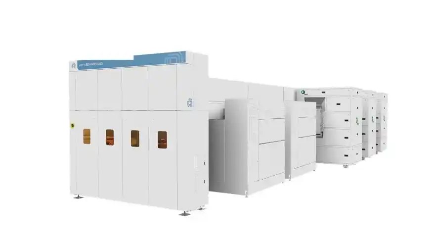
Kinex System (Source: Applied Materials)
Fabs' bets on Hybrid Bonding are also driving BESI's rapid growth. BESI's Q1 2026 orders grew 104.5% year-over-year to 269.7 million euros. Reuters reported the growth was primarily driven by Hybrid Bonding demand, with a second customer from the memory market entering HBM-related qualification.
Second, relaxed standards are also giving TCB a longer lease on life.
According to a TrendForce report in April, JEDEC is reportedly discussing relaxing the next-generation HBM height specification from 775 microns to about 900 microns. This could slow the adoption of Hybrid Bonding. Once the stacking height limit is relaxed, manufacturers can continue using the mature TCB path to support more layers of stacking without immediately taking on the yield risks of Hybrid Bonding.
Finally, TCB equipment is also being upgraded, not standing still.
For example, ASMPT recently launched its AOR TCB technology, focusing on fluxless bonding, active oxide removal, reducing residue contamination, and improving bonding uniformity. The goal is to address challenges in stacking height, precision, and yield for next-generation HBM.
Therefore, a more reasonable industry assessment currently is: In the HBM4/HBM4E stage, TCB and Hybrid Bonding will coexist; by the HBM5 and higher-layer era, Hybrid Bonding's share will likely see a significant increase.
Overall, TCB is not a small trend; it represents a structural change in backend equipment. A related report by Yole points out that backend equipment is transforming from a supporting role in traditional packaging to a strategic equipment market for advanced packaging; among these, TCB and Hybrid Bonding are the two fastest-growing directions. Yole forecasts the TCB market to reach $936 million by 2030, with a CAGR of about 11.6% from 2025-2030; the Hybrid Bonding equipment market is expected to reach $397 million by 2030, with a CAGR of about 21.1%.
Counterpoint's related data also shows that AI GPUs and custom AI ASICs are driving growth in advanced manufacturing and advanced packaging. It predicts that the industry's advanced packaging capacity could expand by about 80% year-over-year in 2026, stating that advanced packaging has become a "gating factor" for AI deployment.
Because of AI, Test Equipment Is Also Facing Bottlenecks
The AI expansion wave is not only causing fabs to scramble for equipment; the equipment suppliers' own supply chains are also being squeezed by shortages of critical components like FPGAs, CPUs, and Driver ICs.
The Elec reported on May 29 that Korean semiconductor test equipment manufacturers are experiencing their "most severe" component shortage ever, with an ironic phrase circulating in the industry: "You can't make semiconductor test equipment without semiconductors." The report stated that lead times for FPGAs used to run test equipment have extended from the past 8-10 weeks to up to 52 weeks at most; Driver ICs, which could previously be purchased immediately from distributors, now require at least a 10-week wait; x86 CPUs and GPUs are also in short supply, with prices for some models rising from around 1 million won to 3 million won, a spike of up to three times.
Because AI data centers are absorbing the production capacity, allocation priority, and inventory buffers for high-end chips, test equipment makers have become the "downstream of the downstream," squeezed out in the allocation of critical components. For example, Sourceability recently noted that FPGA lead times extending to 52+ weeks are mainly due to data center demand. Hyperscale cloud providers and AI infrastructure companies, with their larger orders and stronger bargaining power, are securing higher-priority supply allocations, pushing other industries reliant on similar components to the back of the line. The situation is similar for CPUs and GPUs. While test equipment makers are technologically important, their procurement volumes are difficult to compare with cloud providers and AI server manufacturers.
The shortage logic for Driver ICs differs from that of FPGAs, CPUs, and GPUs. Their scarcity is essentially due to the poor supply elasticity of niche, high-performance analog/mixed-signal devices encountering a surge in test equipment demand. ADI's website lists Automatic Test Equipment as a dedicated product direction, indicating that such chips are specialized critical components within the test equipment supply chain.
The shortage of these critical components is already affecting equipment deliveries. The Elec mentioned that a semiconductor inspection equipment manufacturer recently signed a supply contract worth over 10 billion won with Samsung Electronics but was forced to postpone the delivery by three months due to component shortages. The report also stated that equipment makers have begun discussing equipment quantities and delivery schedules with customers months before the formal PO is issued, in order to secure components early.
Thus, a paradoxical chain has emerged in the AI era: AI chip shortages → fab expansion → need for more test equipment → test equipment requires FPGAs/CPUs/Driver ICs → these chips are prioritized by AI data centers → test equipment delivery delays.
Behind the Frenzied Expansion: Equipment Enters a New Upward Cycle
If the shortages in TCB and test equipment are explosive at individual nodes, zooming out the perspective reveals that the entire semiconductor equipment industry has already entered a new, sweeping, comprehensive upward macro-cycle driven by AI hardware strength.
SEMI forecasts that global semiconductor manufacturing equipment sales will grow from $133 billion in 2025 to $145 billion in 2026 and reach a new historical high of $156 billion in 2027. SEMI specifically noted that this growth is primarily driven by AI-related investments, especially in advanced logic, memory, and advanced packaging.
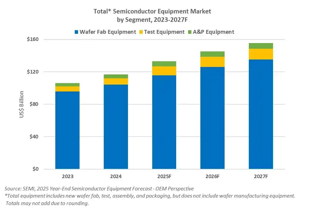
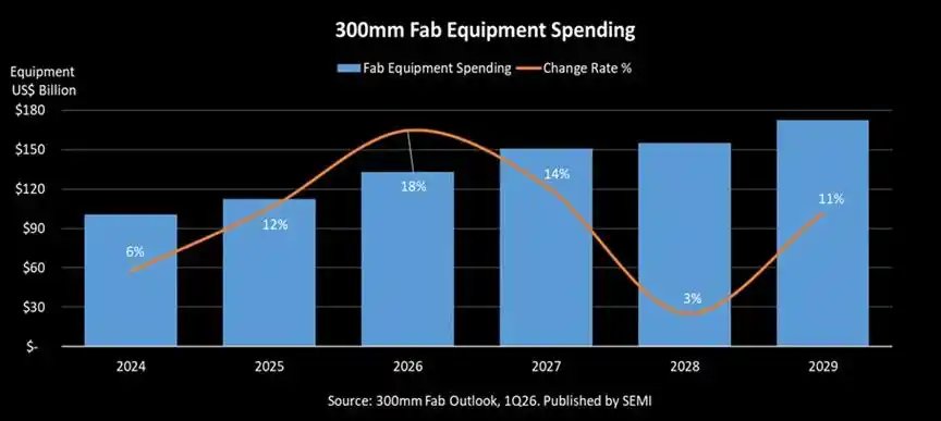
Furthermore, SEMI expects global 300mm fab equipment spending to grow 18% to $133 billion in 2026 and another 14% to $151 billion in 2027, stating that AI is resetting the scale of semiconductor manufacturing investment.
This wave of equipment opportunity mainly stems from three expansion fronts:
First, advanced logic manufacturers TSMC, Intel, and Samsung are all expanding for AI accelerators; TSMC forecasts the global semiconductor market will exceed $1.5 trillion by 2030, with AI and HPC accounting for 55%. Concurrently, TSMC plans to construct nine stages of fabs and advanced packaging facilities in 2026, with 2nm and A16 capacity expected to grow at a 70% CAGR from 2026-2028.
Second, in the memory sector, HBM has reignited the DRAM expansion cycle; SK hynix Chairman Choi Tae-won stated in Taipei in June that SK hynix plans to double its overall wafer capacity within the next five years and believes global memory supply bottlenecks may persist until 2030. According to Counterpoint data, SK hynix held a 58% share of the global HBM market in Q1 2026. In Q1 2026, SK hynix's profits surged significantly, stating that customer demand for HBM supply far exceeds its capacity for the next three years. The company also stated it would significantly increase investment, focusing on M15X expansion, the Yongin cluster construction, and key equipment.
In March of this year, SK hynix disclosed plans to purchase approximately 11.95 trillion won worth of EUV equipment from ASML, with transactions to be completed by the end of 2027 for new product mass production. Analysts believe this equipment will be used for the Yongin factory and the Cheongju M15X factory, covering HBM and advanced DRAM production.
Micron stated in its earnings materials that it is raising its FY2026 capital expenditure plan from $18 billion to approximately $20 billion, primarily to support HBM supply capabilities and 1-gamma DRAM supply, and that it is placing equipment orders ahead of schedule and accelerating installation.
Third, Advanced Packaging: CoWoS, C2S, and C2W are becoming bottlenecks for AI chip delivery; In the AI era, advanced packaging equipment is becoming one of the segments with the highest elasticity in this cycle. TSMC disclosed that CoWoS capacity is expected to grow at a CAGR exceeding 80% from 2022-2027, and wafer demand for AI accelerators is projected to increase 11-fold from 2022-2026.
Therefore, in the semiconductor equipment field, AI computing demand is reopening a major equipment cycle encompassing front-end, back-end, test, and facility equipment.
Conclusion
Today, leading semiconductor equipment companies are not merely selling cold machinery, precise optics, or complex algorithms. What they are selling is essentially the most scarce resource for fabs and tech giants—the capacity realization capability in the AI era.
In this reshuffling game of pricing power, not all equipment suppliers will share the spoils equally. The true winners are the absolute top players firmly positioned at critical process nodes such as advanced logic technology, HBM stacking, advanced packaging (e.g., CoWoS), and high-end chip testing. Holding irreplaceable technological barriers and the keys to capacity, they are rewriting the semiconductor industry's profit distribution landscape with unprecedented posture.
This article is from the WeChat public account "Semiconductor Industry Watch" (ID: icbank), author: Du Qin DQ