Glass Substrate Suddenly Accelerates

marsbitXuất bản vào 2026-06-25Cập nhật gần nhất vào 2026-06-25

Tóm tắt

The adoption of glass substrates in the semiconductor industry is accelerating unexpectedly. Following collaboration announcements between BOE and Corning in late May, and earlier moves by Intel and TSMC, the market for related upstream companies has surged. Intel's "Glass Core Substrate" aims to replace the IC substrate between the circuit board and the chip, primarily addressing thermal warping issues in large AI chips. TSMC's focus is on replacing the expensive silicon interposer layer within the chip package to significantly reduce costs. While initially cautious, with timelines stretching towards 2030, progress has been dramatically pulled forward. Key drivers are NVIDIA, whose ever-larger GPUs like the upcoming Rubin make glass substrates a necessity, and the display panel industry. Companies like Innolux and BOE, leveraging their extensive experience and production lines in panel-grade glass substrates, are rapidly retooling for semiconductor packaging. Innolux has already established production lines and secured orders, while BOE has built pilot lines and is sampling customers. Although technical hurdles remain, such as advanced multi-layer glass processing and copper electroplating, the path to commercialization is now clearer. Large-scale adoption is estimated to begin by late 2027, marking glass substrates as a critical next step in supporting advancing AI computing power.

The AI computing power market is advancing in waves, with gains moving from one segment to another, and now it's the turn of glass substrates.

In late May, BOE announced a memorandum of cooperation with Corning on glass substrates, completely igniting the market.

Not only did its own steady stock price suddenly spike "like a jolt from a heartbeat monitor," with two consecutive trading days of limit-up gains, but upstream companies like Rainbow Display and Wufang Optoelectronics also hit the daily limit-up, Dier Laser's stock price reached a record high, and Vogo Optoelectronics has surged nearly 300% over the past two months.

Institutions have identified 2026 as the first year for commercial validation of glass substrates. Besides the cooperation between BOE and Corning, Intel announced successful mass production of glass core substrates in its latest server CPUs, and TSMC revealed the establishment of a glass substrate CoPoS packaging trial production line.

The two giants are pushing hard, setting the stage perfectly for the bullish atmosphere.

It must be said that the commercialization speed of glass substrates has already exceeded most people's expectations.

Replacing the "Board" in Chips

Intel and TSMC are the current top promoters of glass substrates, but the "glass substrates" they refer to are not exactly the same thing.

A chip is composed of various components mounted on carrier substrates, forming functional units. These functional units are then mounted on the next layer of carrier substrate, creating a larger functional unit, and so on, presenting a hierarchical structure.

For example, the most familiar circuit board is the bottom-most carrier substrate. Further up, there are core substrates, IC substrates, and so on.
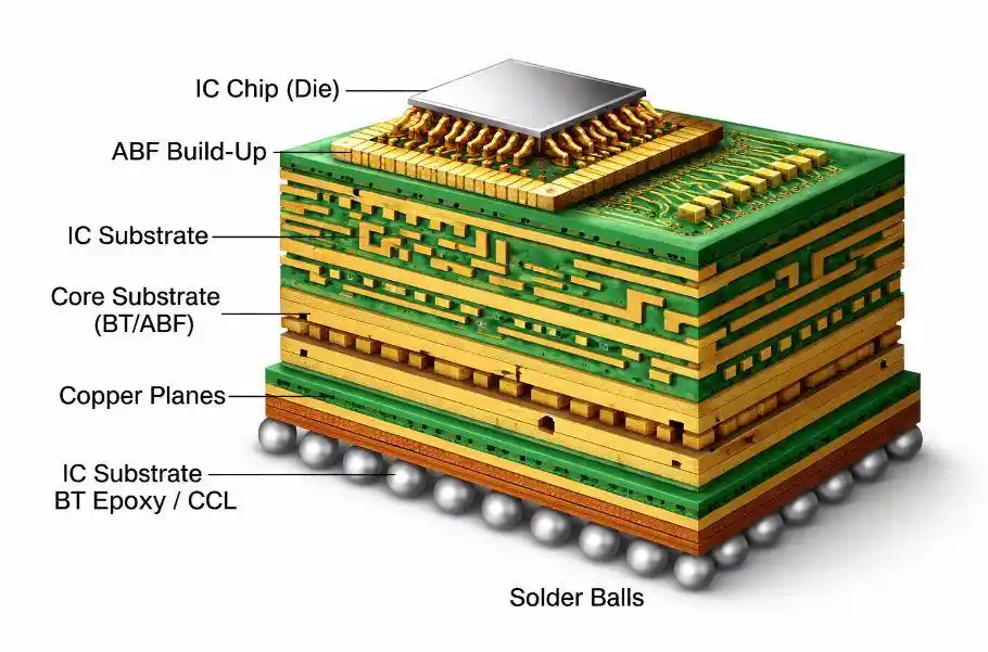
Different layers of "boards" inside a chip; Image source: IC Components

These carrier substrates were traditionally mostly made of materials like resin, fiberglass, copper foil, silicon, etc. As the name suggests, a glass substrate uses glass as the primary material for the substrate.

What Intel and TSMC aim to do is replace mainstream carrier substrates with glass substrates, but they are not targeting the same "board."

Intel's "advanced packaging glass substrate," officially named "Glass Core Substrate," replaces the IC substrate layer between the circuit board and the chip.
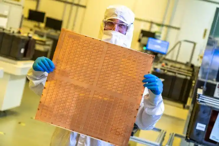
A test glass core substrate displayed by Intel

Currently, mainstream AI chips, including Nvidia GPUs, use substrates primarily made of ABF material. The biggest drawback is their tendency to warp and deform when heated. A one-meter-long ABF carrier substrate expands about 15 micrometers for every 1°C increase in temperature.

In contrast, the silicon chip placed on top of the ABF substrate shows almost no deformation when heated.

Thus, when heat is generated during chip operation, the bottom ABF substrate expands outward due to heat, while the upper silicon chip remains unchanged, causing the entire substrate to bend or "warp."

The larger the chip size, the more severe the warping becomes—imagine a credit card with all four corners curling up simultaneously. The consequences could be catastrophic.
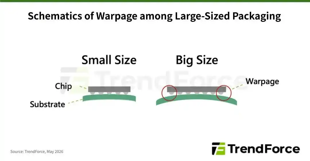
The larger the carrier substrate size, the more obvious the warping; Image source: TrendForce

This is why glass substrates are being considered. Due to their "heat resistance" being comparable to silicon chips, even if they deform at high temperatures, they can maintain synchronization with the silicon chip, effectively preventing warping.

Compared to Intel, TSMC wants to replace a carrier substrate located one layer higher—the bare die layer of the chip.

A GPU bare die consists of computing core units (CPU/GPU) and multiple HBM stacks, placed on a silicon interposer. This silicon interposer is the "board" TSMC most wants to replace.
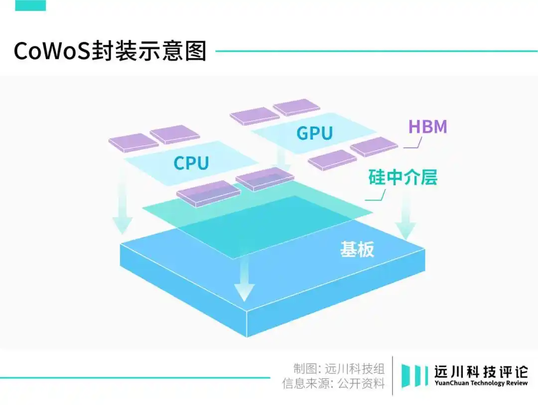
The manufacturing cost of a silicon interposer is extremely high, with a unit price exceeding $100 for a large-size silicon interposer [2]. For comparison, the A19 Pro chip in the iPhone 17 Pro Max costs only about $90 per unit for procurement.

Moreover, compared to these powerful computing SoCs for phones, the silicon interposer's main function is merely data transfer, akin to buying a scooter for the price of a sports car, which sounds even worse.

The size of the silicon interposer is directly related to the size of the AI chip and the number of HBM stacks used. As AI chips become larger and more HBM is used, the cost sinkhole for silicon interposers deepens.

For companies purchasing AI chips, it's like buying a car for $100,000 and having to spend an additional $50,000 on a license plate to drive it.

Replacing the silicon interposer with a glass substrate offers the biggest advantage: cost. For the same size, it costs less than half of the silicon counterpart [2].

The ideas from Intel and TSMC are both reasonable, but the implementation of new technology is never a simple order. Especially in the chip industry, new technology challenges not just the laws of physics.

Chip manufacturing is humanity's most complex activity to date, having solidified over the past half-century into an extremely strict set of rules. The upstream and downstream segments have meticulously built a standardized system where everything is tightly interlocked; a small adjustment can affect everything.

Even the slightest adjustment may lead to changes or complete overhauls in upstream equipment and materials.

Hence, while giants talk boldly about innovation, their actions remain conservative and cautious.

Intel proposed the glass core substrate concept in 2023, with mass production vaguely scheduled for sometime between 2026 and 2030. TSMC has been secretive about its CoPoS plan, only recently revealing for the first time that it would take 2-3 years to scale up to a certain size.

However, a few big hands have forcefully yanked the progress bar forward by a large margin.

Who is Pulling the Progress Bar?

The first big hand is Nvidia.

Just a few months after Intel announced the glass core substrate, Morgan Stanley released a report predicting that GB200 "might" use glass substrates for packaging.

This report was once overinterpreted as "Nvidia officially announced GB200 will use glass substrates," causing another surge in related concept stocks.

Putting the misunderstanding aside, the fact that an unsupported speculation could have such strong persuasive power is because, in the public's perception, Nvidia indeed has the greatest motivation to push glass substrate adoption.

Nine out of ten AI computing power chips are Nvidia GPUs. Bearing the weight of exponentially increasing computing demands, each GPU generation strives to pack more transistors, leading to larger and larger GPUs.

The B200's area is nearly double that of its predecessor, the H100, almost 10 times the size of Apple's M2 Ultra chip, roughly half the size of a bank card, already pushing the warping limits of ordinary IC substrates.

The upcoming Rubin, set for mass production in the second half of the year, is even larger than the B200. Changing materials is not an option but a necessity.
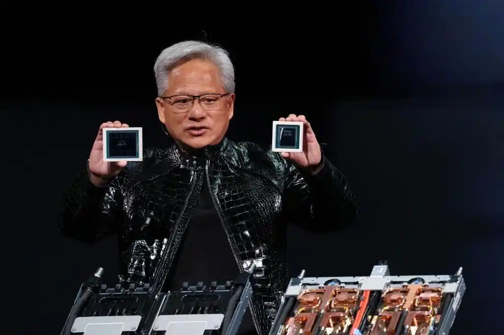
Jensen Huang holding B200 (left) and H100 (right)

In March this year, Nvidia announced a full shift to glass substrates, with Rubin leading the trial, fast-forwarding the commercialization timeline to the end of this year.

With Nvidia's big hand pulling from the front, an unexpected big hand is pushing from behind. It's not from the upstream chip industry, but from a neighboring sibling industry—display panels.

Before being used in chip packaging, the largest downstream application for glass substrates was display panels.

A display panel has a sandwich structure internally, with the two "slices of bread" being glass substrates—one controlling brightness, the other controlling color.
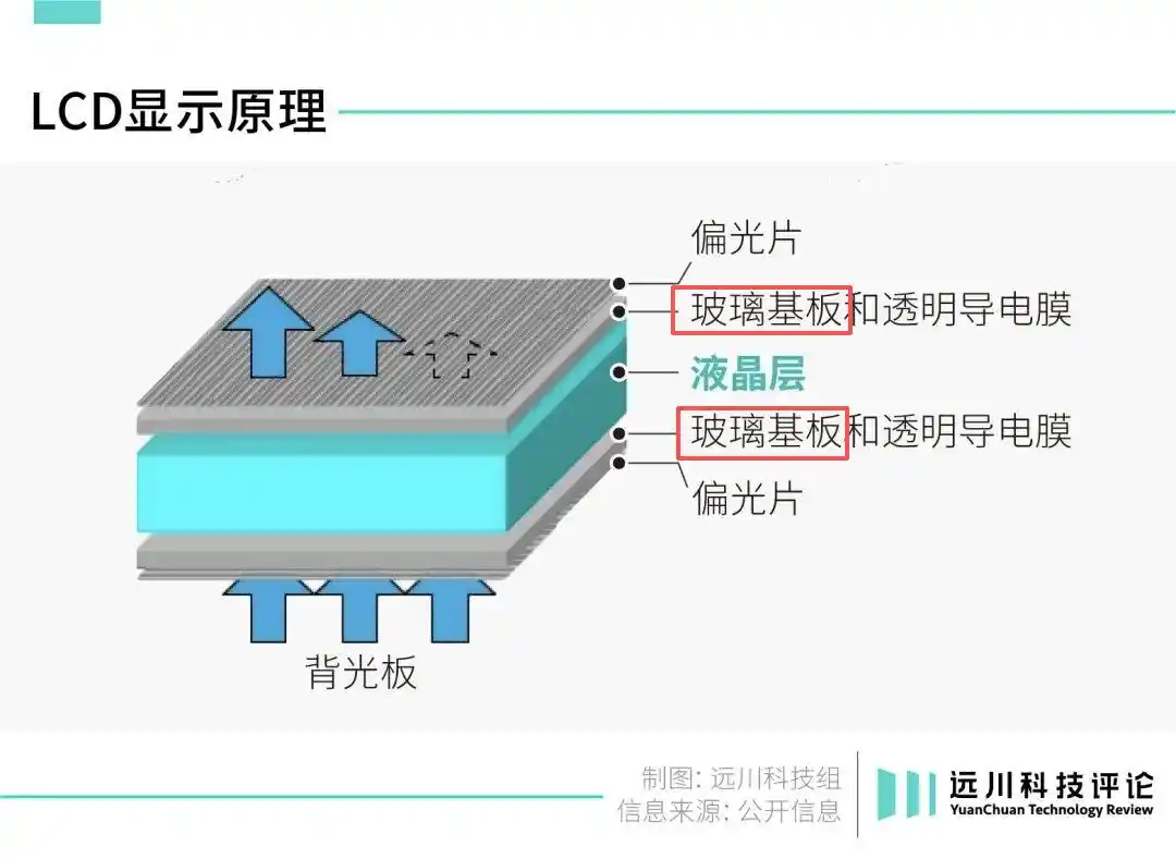
Glass substrates in an LCD panel

The precision processing technologies and equipment used here have extremely high overlap with those needed for glass substrates in chips. Exaggerating a bit, high-end production lines can be modified for use.

Therefore, regarding glass substrate implementation, the most enthusiastic are actually brothers from the panel industry.

For example, Taiwan's major panel maker Innolux plotted a transition to chip packaging as early as 2019.

With a global panel price war raging fiercely, Innolux, seeing it couldn't hold out, accepted an olive branch from Taiwan's Industrial Technology Research Institute (ITRI) to jointly develop glass substrate-based chip packaging technology, modifying its own panel production lines.

By the time Intel announced glass substrate technology in 2023, Innolux had already built the world's first FOPLP packaging production line converted from a panel line.

The following year, it secured major orders from chip giants NXP and STMicroelectronics, and sold an idle 5.5-generation panel line at a high price to TSMC to alleviate the latter's shortage of advanced packaging capacity.

By early this year, Innolux's FOPLP advanced packaging line had increased monthly production tenfold to tens of millions, not only firmly embracing TSMC's leg but reportedly also entering SpaceX's Starlink supply chain.

Taiwan's panel makers work fiercely hard, and progress on the mainland side is equally rapid.

BOE began researching and developing glass substrates in 2020, invested nearly 1 billion yuan in building a pilot line in 2024, and achieved fully automated equipment operation in the first half of this year [4].

It has already started sending samples to customers for testing and validation. The cooperation with Corning in May was to lock in future years of upstream specialty glass supply, with large-scale mass production imminent.

Mainland China holds over 60% of global panel capacity, especially in high-generation panels with the world's most mature and highly automated production lines. A bigger advantage lies in having a complete upstream industry chain for support.

Several companies currently of most interest in the secondary market, such as Dier Laser, Han's Laser, and Delong Laser, are upstream manufacturers of TGV (Through Glass Via) laser microvia equipment. Vogo Optoelectronics is midstream, handling glass substrate processing.

Beyond Chinese manufacturers, Korea's Samsung Electro-Mechanics, LG Innotek, Japan's Dainippon Printing, and Nippon Electric Glass are all active proponents of glass substrates—familiar faces from the panel wars.

With downstream demand secured by big spenders and upstream sibling industries providing warm support, glass substrates have quickly progressed from being seriously criticized as "concept hype" to the "eve of mass production." Securities firms have changed their cautious stance, drawing bigger and bigger pies.

Objectively speaking, there are still several technical hurdles to overcome before glass substrates achieve large-scale implementation.

For example, the core material—specialty glass—currently only Corning can process up to 11 layers without cracking, while the domestic supply chain can manage at most 3-4 layers [5]. Other issues include insufficient copper electroplating equipment and processes [5].

According to industry chain estimates, the earliest large-scale volume production for glass substrates will likely be by the end of 2027.

The end of computing power is electricity, but before reaching that end, the industry chain must cross another hurdle—perhaps one more glass substrate.

References

[1] Research on Warpage of 2.5D CoWoS Packaging Based on Glass Substrate, Shi Hangbo, Wang Xu, Fan Jilei, et al.

[2] Large Silicon Interposer Unit Price Exceeds $100, Accounting for Half the Cost; How Can AI Computing Chips Break Through the Packaging Cost Bottleneck? Yue Tou Gu

[3] Complete Breakdown of TGV Glass Via: After Intel's Glass Substrate Entry, Understanding the Hard Barriers, 2027 Mass Production Countdown, and Taiwan Supply Chain Investment Map, Sinopac Securities

[4] BOE: Glass Substrate Packaging Carrier Pilot Line Operational, Design Capacity 1000 Sheets/Month, Future Semiconductor

[5] Glass Substrate Industry Exchange, Summary Research Report

This article is from the WeChat public account "Yuanchuan Technology Review" (ID: kechuangych), author: He Lüheng, editor: Li Motian

Tiền kỹ thuật số thịnh hành

Câu hỏi Liên quan

QWhat are the two main applications of glass substrates in the chip industry, as promoted by Intel and TSMC respectively?

AIntel promotes the use of 'Glass Core Substrate' to replace the IC substrate layer (between the circuit board and the chip). TSMC aims to use glass substrates to replace the silicon interposer layer (within the chip's bare die layer).

QWhy is the transition to glass substrates becoming increasingly necessary for high-performance AI chips like NVIDIA's GPUs?

AAs AI GPUs become larger (e.g., B200, Rubin) to pack more transistors, the traditional organic ABF substrates are prone to warping due to heat. Glass substrates have thermal properties similar to silicon, preventing this warping and enabling larger chip designs.

QWhich non-semiconductor industry is playing a significant role in accelerating the adoption of glass substrates for chip packaging, and why?

AThe display panel industry is a key accelerator. Companies like Innolux and BOE are repurposing their mature, high-precision panel manufacturing lines and expertise for glass substrate processing, providing ready-made production capacity and supply chain support.

QWhat is the primary benefit for TSMC in replacing silicon interposers with glass substrates in its CoWoS packaging?

AThe primary benefit is significant cost reduction. Large silicon interposers are extremely expensive (over $100 each), while similarly sized glass substrates are estimated to cost less than half that amount.

QAccording to the article, what are some of the key technical challenges that still need to be overcome before glass substrates can achieve mass adoption?

AKey challenges include: 1) Developing special glass materials that can withstand multiple layers (e.g., 11+) of processing without breaking; 2) Improving copper electroplating equipment and processes for creating high-quality interconnects within the glass substrate.

Nội dung Liên quan

Đối thoại với đồng sáng lập Hyperdash: Tại sao Hyperliquid vẫn bị đánh giá thấp một cách nghiêm trọng?

Nguồn: The Rollup | Biên tập: Felix, PANews Hanson Birringer, đồng sáng lập kiêm Giám đốc Doanh thu của Hyperdash - nền tảng phân tích dữ liệu giao dịch trên Hyperliquid, gần đây đã chia sẻ trong podcast "The Rollup" về cách Hyperliquid xây dựng một tầng thanh khoản phi tập trung và hiệu quả thông qua việc kết hợp ba xu hướng lớn: hợp đồng vĩnh cửu (perp), Tài sản Thế giới Thực (RWA) và stablecoin. Ông nhấn mạnh Hyperliquid là một hệ sinh thái mã nguồn mở, không cần cấp phép và phi tập trung, kết hợp tinh thần của crypto với hiệu suất tài chính cao, thu hút cả vốn tổ chức. Hyperliquid được coi là biểu hiện thuần túy nhất của ba siêu xu hướng trên. Đặc biệt, việc tích hợp USDC làm tài sản định giá cốt lõi và cơ chế chia sẻ 90% doanh thu từ lãi suất trái phiếu kho bạc vào quỹ hỗ trợ để mua lại token HYPE một cách lập trình đã tạo ra áp lực mua hàng tỷ USD, bên cạnh phí giao dịch. Hyperliquid cũng đang chủ động đối mặt với thách thức quy định thông qua trung tâm chính sách, hợp tác với các ví như Phantom để vận động hành lang các cơ quan quản lý Mỹ (như CFTC), mở đường cho các nền tảng môi giới truyền thống kết nối trực tiếp. Sự ra mắt của sản phẩm ETF Hyperliquid bởi Grayscale, với sự hỗ trợ từ quỹ SPV Hyper Holdings Global, cung cấp kênh đầu tư phù hợp và dễ tiếp cận cho các tổ chức. Về tăng trưởng doanh thu, tiềm năng là rất lớn nếu các hợp đồng vĩnh cửu RWA có thể thu hút một phần nhỏ khối lượng giao dịch toàn cầu, kéo theo sự mở rộng quy mô ký quỹ và lợi ích từ stablecoin. Việc Hyperdash mua lại công ty dữ liệu Imperator giúp cung cấp công cụ và gói dữ liệu cấp doanh nghiệp mạnh mẽ hơn cho cả nhà giao dịch retail và các công ty quản lý quỹ truyền thống. Nhìn chung, lạc quan về tương lai của Hyperliquid dựa trên xu hướng phổ cập tài chính toàn cầu thông qua điện thoại thông minh. Khó có thể tìm thấy kịch bản tiêu cực trừ khi các xu hướng dài hạn về phổ cập internet và tài chính bị đảo ngược.

marsbit1 giờ trước

Đối thoại với đồng sáng lập Hyperdash: Tại sao Hyperliquid vẫn bị đánh giá thấp một cách nghiêm trọng?

marsbit1 giờ trước

Phiên bản ‘đầy đủ máu’ DeepSeek V4 đã lộ diện, có thể ra mắt sớm nhất vào ngày mai

DeepSeek V4 phiên bản đầy đủ (“Full Blood”) đã lộ diện và có thể được ra mắt sớm nhất vào ngày mai. Bài viết cho biết sau gần ba tháng chờ đợi, phiên bản chính thức của DeepSeek V4 (GA) sắp được phát hành, với hai biến thể: V4 Flash và V4 Pro. Hiện một số người dùng đã có quyền truy cập thử nghiệm. Một mẹo kiểm tra là xem lập luận (CoT) của mô hình bắt đầu bằng “I’m” thay vì “Let me” như phiên bản cũ. Theo đánh giá ban đầu từ các nhà phát triển, hiệu năng tổng thể của V4 tiếp cận mức Claude Opus 4.8, khả năng lập trình ngang ngửa GPT-5.6 Sol, và kỹ năng Agent, tạo 3D/SVG được cải thiện rõ rệt. Tuy nhiên, nó vẫn có thể không vượt mặt Kimi K3 mới ra mắt. Điểm đáng chú ý là chiến lược định giá. DeepSeek lần đầu giới thiệu cơ chế tính phí theo giờ cao điểm/thấp điểm. Cụ thể, V4 Pro có giá 0.87 USD cho triệu token xuất (cao điểm: 1.74 USD), còn V4 Flash chỉ 0.28 USD (cao điểm: 0.56 USD). Dù có tăng giá so với trước, mức giá này vẫn cạnh tranh mạnh so với các đối thủ như Fable 5 (50 USD/triệu token xuất). Như vậy, DeepSeek V4 có thể không phải là mô hình mạnh nhất mọi mặt, nhưng tiếp tục duy trì chiến lược “kẻ hủy diệt giá” bằng cách cung cấp hiệu năng cao với mức giá thấp đáng kể, tạo ra một cú hích lớn trong cộng đồng AI.

marsbit1 giờ trước

Phiên bản ‘đầy đủ máu’ DeepSeek V4 đã lộ diện, có thể ra mắt sớm nhất vào ngày mai

marsbit1 giờ trước

Quan sát hàng tuần của WEEX Labs: 'Tái cấu trúc quyền lực' trong cơ sở hạ tầng AI và 'cuộc vận động lặn sâu' vào kinh tế thực

Tháng 7 năm 2026 đánh dấu một bước ngoặt trong ngành công nghiệp AI: **quyền phân bổ năng lực tính toán chuyển dịch từ các gã khổng lồ đám mây sang các chủ sở hữu năng lực tính toán**, và **giá trị cốt lõi của AI tập trung hơn vào việc thâm nhập công nghiệp thực**, thay vì chỉ chạy đua về thông số mô hình. Các biến động chính trong tuần bao gồm: 1. **Bản đồ năng lực tính toán thay đổi:** Meta ra mắt dịch vụ đám mây "MetaCompute", mang đến cuộc cạnh tranh trực tiếp với AWS, Azure và đe dọa không gian sống còn của các nhà cho thuê năng lực tính toán cỡ vừa và nhỏ. 2. **Mô hình mã nguồn mở với chi phí tối ưu:** Các mô hình nền tảng Trung Quốc như DeepSeek-V4 đạt trình độ đỉnh cao và mở rộng mã nguồn, đẩy nhanh quá trình "tiện ích hóa" AI, giúp giảm đáng kể ngưỡng chi phí cho doanh nghiệp và giáo dục. 3. **Trí tuệ hiện thân bước vào nhà máy:** Robot hình người, dưới sự thúc đẩy của chính sách, chuyển từ phòng thí nghiệm sang đào tạo thực tế trong các dây chuyền sản xuất như hậu cần và lắp ráp ô tô. Giá trị đánh giá chuyển từ tính năng sang hiệu quả và sự ổn định trong môi trường công nghiệp. 4. **Quản trị toàn cầu đi vào thực chất:** Khái niệm "AI chủ quyền" trở thành khuôn khổ thực tế, đặt ra các yêu cầu tuân thủ địa chính trị cao hơn, buộc các mô hình AI phải tích hợp sẵn kiến trúc có thể kiểm toán và tôn trọng chủ quyền dữ liệu. **Góc nhìn sâu từ WEEX Labs:** Sự thịnh vượng của AI đang thâm nhập sâu vào cơ cấu sản xuất toàn cầu. Doanh nghiệp nên: - Tận dụng lợi thế mã nguồn mở để xây dựng kho kiến thức riêng tư, tránh phụ thuộc quá mức vào API bên ngoài. - Cảnh giác với rủi ro bị "khóa chặt" vào một nhà cung cấp năng lực tính toán duy nhất. - Tìm kiếm cơ hội trong hệ sinh thái "trí tuệ hiện thân", chẳng hạn như phần mềm mô phỏng công nghiệp hoặc dịch vụ cung cấp giải pháp thích ứng năng lực tính toán AI cho nhà máy.

marsbit1 giờ trước

Quan sát hàng tuần của WEEX Labs: 'Tái cấu trúc quyền lực' trong cơ sở hạ tầng AI và 'cuộc vận động lặn sâu' vào kinh tế thực

marsbit1 giờ trước

WEEX TradFi Có Đáng Tin Cậy Không? Những Điều Bạn Nên Biết Trước Khi Giao Dịch Mã Thông Báo Cổ Phiếu Mỹ Lần Đầu Tiên

Trong vài năm qua, người dùng Crypto ngày càng quan tâm đến các tài sản tài chính truyền thống (TradFi) như cổ phiếu Mỹ (Apple, Microsoft, NVIDIA, Tesla) hay chỉ số NASDAQ. Sự xuất hiện của các token cổ phiếu này trên các nền tảng giao dịch tiền số như WEEX TradFi làm mờ ranh giới giữa hai thị trường. Tuy nhiên, cần hiểu rõ: token cổ phiếu không phải là cổ phiếu thực tế. Người dùng giao dịch biến động giá của tài sản cơ sở, không sở hữu cổ phần hay có quyền biểu quyết, cổ tức. Ưu điểm chính là trải nghiệm quen thuộc cho người dùng Crypto: giao dịch 24/7, tiếp cận nhiều loại tài sản truyền thống chỉ trong một nền tảng. Để đánh giá độ tin cậy của sản phẩm TradFi, người dùng cần tìm hiểu cơ chế định giá, cách theo dõi tài sản cơ sở và các rủi ro đi kèm. Biến động vẫn tồn tại dù giao dịch suốt ngày đêm. Các tài sản như cổ phiếu công nghệ chịu ảnh hưởng từ kết quả kinh doanh, xu hướng ngành và kinh tế vĩ mô. Tóm lại, TradFi đang trở thành cầu nối, cho phép người dùng Crypto khám phá cơ hội toàn cầu trong môi trường quen thuộc. Điều quan trọng nhất trước khi giao dịch là hiểu rõ sản phẩm, cơ chế và quản lý rủi ro phù hợp.

marsbit1 giờ trước

WEEX TradFi Có Đáng Tin Cậy Không? Những Điều Bạn Nên Biết Trước Khi Giao Dịch Mã Thông Báo Cổ Phiếu Mỹ Lần Đầu Tiên

marsbit1 giờ trước

Giao dịch

Giao ngay

Bài viết Nổi bật

Làm thế nào để Mua WAVES

Chào mừng bạn đến với HTX.com! Chúng tôi đã làm cho mua Waves (WAVES) trở nên đơn giản và thuận tiện. Làm theo hướng dẫn từng bước của chúng tôi để bắt đầu hành trình tiền kỹ thuật số của bạn.Bước 1: Tạo Tài khoản HTX của BạnSử dụng email hoặc số điện thoại của bạn để đăng ký tài khoản miễn phí trên HTX. Trải nghiệm hành trình đăng ký không rắc rối và mở khóa tất cả tính năng. Nhận Tài khoản của tôiBước 2: Truy cập Mua Crypto và Chọn Phương thức Thanh toán của BạnThẻ Tín dụng/Ghi nợ: Sử dụng Visa hoặc Mastercard của bạn để mua Waves (WAVES) ngay lập tức.Số dư: Sử dụng tiền từ số dư tài khoản HTX của bạn để giao dịch liền mạch.Bên thứ ba: Chúng tôi đã thêm những phương thức thanh toán phổ biến như Google Pay và Apple Pay để nâng cao sự tiện lợi.P2P: Giao dịch trực tiếp với người dùng khác trên HTX.Thị trường mua bán phi tập trung (OTC): Chúng tôi cung cấp những dịch vụ được thiết kế riêng và tỷ giá hối đoái cạnh tranh cho nhà giao dịch.Bước 3: Lưu trữ Waves (WAVES) của BạnSau khi mua Waves (WAVES), lưu trữ trong tài khoản HTX của bạn. Ngoài ra, bạn có thể gửi đi nơi khác qua chuyển khoản blockchain hoặc sử dụng để giao dịch những tiền kỹ thuật số khác.Bước 4: Giao dịch Waves (WAVES)Giao dịch Waves (WAVES) dễ dàng trên thị trường giao ngay của HTX. Chỉ cần truy cập vào tài khoản của bạn, chọn cặp giao dịch, thực hiện giao dịch và theo dõi trong thời gian thực. Chúng tôi cung cấp trải nghiệm thân thiện với người dùng cho cả người mới bắt đầu và người giao dịch dày dạn kinh nghiệm.

Tổng lượt xem 401Xuất bản vào 2024.12.11Cập nhật vào 2026.06.02

Làm thế nào để Mua WAVES

Thảo luận

Chào mừng đến với Cộng đồng HTX. Tại đây, bạn có thể được thông báo về những phát triển nền tảng mới nhất và có quyền truy cập vào thông tin chuyên sâu về thị trường. Ý kiến ​​của người dùng về giá của WAVES (WAVES) được trình bày dưới đây.

活动图片