18 Months, Over 50x Surge: KIOXIA's Epic Comeback

marsbitXuất bản vào 2026-06-23Cập nhật gần nhất vào 2026-06-23

Tóm tắt

KIOXIA, a NAND flash memory giant, staged a dramatic comeback driven by AI demand. After a period of significant losses, a failed merger, and missed HBM opportunities, its 2024 IPO began modestly. However, fueled by explosive demand for AI data storage, its stock price skyrocketed over 50 times within 18 months, making it Japan's most valuable company, surpassing Toyota. Its Q1 FY2026 profit guidance soared 30-fold year-over-year, with 2026 NAND capacity already sold out. Key to its success is its 3D NAND technology, BiCS FLASH. As the inventor of NAND, KIOXIA advanced its technology through generations, reaching over 200 layers by 2023. Key innovations include CBA (CMOS directly Bonded to Array), which separately manufactures control circuits and memory arrays for better performance, and OPS (On Pitch Select Gate) to increase density. The company is now developing high-capacity packages like an 8TB solution stacking 32 dies. Looking beyond NAND, KIOXIA is exploring 3D DRAM with its OCTRAM technology, using oxide semiconductor transistors for ultra-low leakage to reduce power consumption. This fundamental research differs from HBM and represents a long-term bet to extend its 3D expertise from NAND into future DRAM architectures. KIOXIA's story highlights how technological assets and shifting market cycles can rapidly transform a company's fortunes. While questions remain about sustaining growth beyond the current AI boom, its resurgence demonstrates that in semiconductors,...

Author: Du Qin DQ

Previously, we have deeply analyzed this flash memory giant's regrettable trough period in another article: burdened by the past glory of Toshiba Memory but 'born at the wrong time'; cold-shouldered by the capital markets, leading to a last-minute IPO setback; suffering consecutive huge losses in an industry downturn, and unfortunately missing out on the enormous opportunity of HBM, with even its attempt to seek refuge through a merger with Western Digital falling through... At that time, KIOXIA seemed to have become a 'hot potato' in the eyes of outsiders amid the semiconductor industry reshuffle.

However, just over a year later, KIOXIA staged a comeback that can be described as epic. Driven by the frenzy of AI large models, the market logic for storage underwent a fundamental shift. KIOXIA not only successfully reversed its fortunes but also achieved a dual explosion in both capital markets and technology.
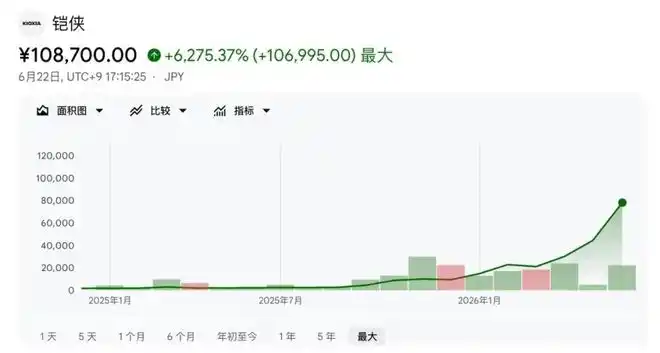
KIOXIA's stock price trend since listing

The Super Myth in the Capital Markets

KIOXIA successfully listed on the Tokyo Stock Exchange at the end of 2024, with its initial market capitalization hovering around only 800 billion yen (approximately $50 billion). However, with the comprehensive explosion of AI storage demand, KIOXIA performed an epic reversal in the 18 months following its listing: its stock price skyrocketed over 50 times within 18 months, rising 8-fold in 2026 alone.

Currently, KIOXIA's market capitalization has exceeded 51 trillion yen (approximately 481 trillion Korean won), repeatedly surpassing Toyota Motor, the symbol of Japanese manufacturing, to become the highest-valued company on the Japanese stock market.

According to KIOXIA's Q1 FY2026 (April–June) earnings forecast, its quarterly operating profit is expected to reach as high as 1.3 trillion yen (approximately $81 billion), a staggering increase of nearly 30 times year-over-year; the quarterly net profit guidance is 869 billion yen, a 48-fold increase year-over-year. The performance of a single quarter surpassed the full-year net profit forecast for FY2025.

As major customers scrambled to sign long-term supply contracts, KIOXIA's 2026 NAND capacity has been completely sold out, and the supply-demand imbalance is expected to persist until 2027. The market anticipates KIOXIA's operating profit margin this year to exceed 60%, setting a record for the highest profitability level in the global memory industry. Furthermore, with market expectations for shareholders to receive returns such as stock splits and dividends, its target stock price is hoped to rise to 200,000 yen.

This wave of soaring value has delivered investment returns beyond imagination to parent company Bain Capital, which held on during the downturn, and indirect major shareholder SK Hynix.

According to the Financial Times, the AI boom has made Bain's 2018 acquisition of Toshiba Memory (now KIOXIA) one of the most profitable private equity deals in history. Bain Capital has realized profits by selling most of its shares, with returns exceeding $150 billion, a near 20x return on investment. Its flagship private equity fund is estimated to have gained over $8 billion in profit.

SK Hynix invested a total of 395 billion yen (approximately 3.9 trillion Korean won at the time) in Toshiba Memory in 2018 through a consortium involving Korea, the US, and Japan, among other forms. Currently, this consortium still holds an 18% stake in KIOXIA. With the surge in KIOXIA's stock price, SK Hynix has seen enormous paper gains, and the market expects the consortium's eventual total profit to far exceed $70 billion.

The former 'hot potato' instantly transformed into a 'super ATM'.

In the past, the benefits of artificial intelligence were mainly concentrated in GPU and HBM companies like NVIDIA and SK Hynix. HBM was the star on the AI training side, while NAND became a scarce resource in AI inference, model storage, data lakes, enterprise SSDs, and nearline storage. The market expects KIOXIA's net profit for FY2027 to reach 2.8389 trillion yen, a 5.1-fold increase compared to the previous year.

3D NAND, The Foundation of KIOXIA's Existence

KIOXIA invented NAND flash memory over 35 years ago. In 2007, KIOXIA introduced BiCS FLASH 3D flash memory, a 3D flash memory technology system centered around vertical stacking, lateral scaling, wafer bonding, select gate optimization, and advanced packaging.

The basic idea of 3D NAND is: unlike 2D NAND, which only shrinks cells on a plane, it stacks memory cells vertically like building a skyscraper. KIOXIA's explanation is vivid: originally it was one floor with limited land area; 3D NAND is equivalent to turning a one-story building into a multi-story apartment, accommodating more 'residents' on the same area.

The core of BiCS FLASH is its batch processing technology. Its general process logic is: first, alternately stack plate-like electrodes and insulating layers; then drill a large number of holes along the vertical direction in one go; next, fill the holes with charge storage films and pillar-like electrodes; the intersection of the plate-like electrode and pillar-like electrode forms a memory cell. This shows that KIOXIA's BiCS FLASH is not the traditional 'create memory cells separately for each added layer,' but rather stacks the structure first, then forms memory cells by 'punching and plugging' through multiple layers at once. Therefore, when the number of layers increases, the manufacturing cost does not rise completely linearly, improving the economic viability of continued stacking for 3D NAND.

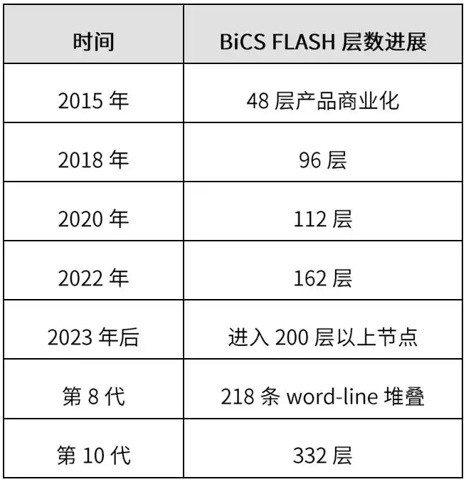
KIOXIA's officially disclosed commercialization timeline for BiCS FLASH is roughly as follows: BiCS FLASH products achieved commercialization with 48 layers in 2015, then progressed to 96 layers, 112 layers, 162 layers; as of March 2023, stacking of over 200 layers has been achieved.

Among these, the 8th-generation BiCS FLASH is a key milestone. KIOXIA states that the 8th-generation product uses 218 word-line stacks, achieves a storage density of 18.3Gb/mm² for the 1Tb TLC product, and supports a 3.2Gbps external data transfer speed, 40μs read time, and 205MB/s programming throughput.

KIOXIA's 8th-generation BiCS FLASH not only jumped from 162 layers to 218 layers but also introduced two key technologies:

CBA (CMOS directly Bonded to Array): CBA can be understood as manufacturing the peripheral CMOS control circuit and the memory array separately, followed by wafer bonding. In the past, CMOS circuits and the memory array were manufactured on the same wafer. However, the optimal process conditions for both are not identical: the memory array may require processes better suited for charge storage and stacked structures, while CMOS circuits focus more on logic control, electrical performance, and speed. Manufacturing them on the same wafer forces compromises.

CBA's approach is: manufacture the CMOS wafer separately, manufacture the memory array wafer separately, optimize the processes for each independently, and finally bond them together with high precision. The benefits are: improved bit density, increased NAND I/O speed, allowing the memory array to use high-temperature processes previously limited by CMOS constraints, and reduced electrical interference between adjacent memory cells.

OPS (On Pitch Select Gate): OPS solves the problem of wasted space within the memory array. In traditional structures, there exist 'dummy' areas between memory cells that are not used for data storage. These areas do not directly contribute to capacity but occupy area. KIOXIA's OPS technology, by rearranging select gates and insulating isolation structures, reduces or eliminates these ineffective areas, allowing more effective memory cells to be placed in the same area. KIOXIA's official explanation states that OPS removes unnecessary dummy regions, enabling more actual memory cells to be placed in the same space, significantly improving storage density.
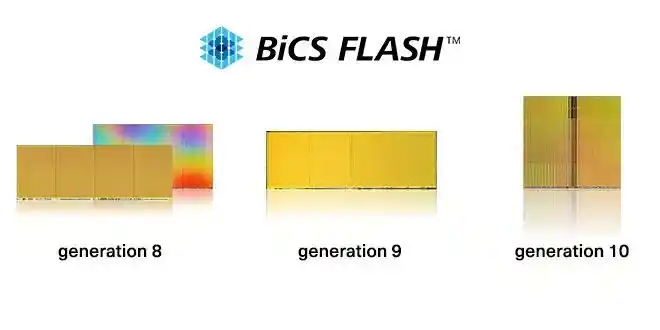
The 9th-generation BiCS FLASH primarily targets 512Gb and 1Tb TLC products, positioned to support applications in the mid-to-low capacity range that require high performance and low power consumption. It continues to use CBA and OPS technologies to improve production efficiency and provide more advanced flash memory solutions. The 9th generation does not follow the route of increasing layer count but emphasizes the balance between performance, power consumption, cost, and production efficiency.

The 10th-generation BiCS FLASH clearly leans more towards future high-capacity, high-performance demands. KIOXIA states that the 10th-generation product uses the same CMOS technology as the 9th generation while increasing the number of memory layers to 332, approximately 1.5 times that of the 8th generation, to enhance bit density and power efficiency.
Beyond front-end manufacturing processes, KIOXIA is also advancing back-end packaging capabilities. Official materials mention that KIOXIA developed a single-package 8TB flash memory, achieved by stacking 32 flash memory dies, each 2Tb, within one package. This relies on advanced back-end processes like wafer thinning, material design, and wire bonding. This 32-die stacking can assemble 32 pieces of 2Tb dies into a package with a height under 2mm, forming an 8TB flash memory solution.

From 3D NAND to 3D DRAM, KIOXIA's New Gambit

KIOXIA is also deploying a secret weapon to break through the single-product-line barrier of being a 'pure NAND vendor.' Why is KIOXIA venturing into 3D DRAM? This is because DRAM has also reached a planar scaling bottleneck similar to what NAND faced. As an established player in 3D NAND, KIOXIA also possesses process-validated advantages.

Continued scaling of traditional DRAM encounters several challenges: storage capacitors become increasingly difficult to shrink, access transistor leakage increases, data retention time shortens, refresh frequency rises, and higher capacity leads to higher refresh power consumption. Imec also mentioned in a technology review that the traditional DRAM 1T1C structure faces scaling, cost, and power efficiency challenges, especially as large capacitors limit the 3D integration path, and smaller transistors lead to more pronounced leakage paths, causing increased refresh power consumption.

In December 2024, KIOXIA announced the development of OCTRAM (Oxide-Semiconductor Channel Transistor DRAM) technology, a new 4F² DRAM composed of oxide semiconductor transistors, offering both high on-current and ultra-low off-current. This achievement was jointly developed by KIOXIA and Nanya Technology and presented at the 2024 IEEE IEDM.
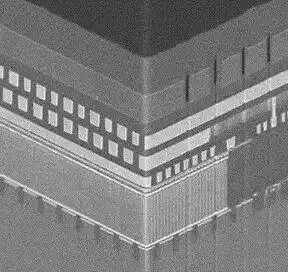
Panoramic view of OCTRAM (Source: KIOXIA, same below)

Traditional DRAM cells are generally 1T1C, meaning one access transistor plus one capacitor. Its problem is: as the cell continues to shrink, the capacitor becomes harder to make, and transistor leakage also increases refresh power consumption. KIOXIA's OCTRAM attempts to reduce leakage through InGaZnO transistors and push the cell structure towards higher density.
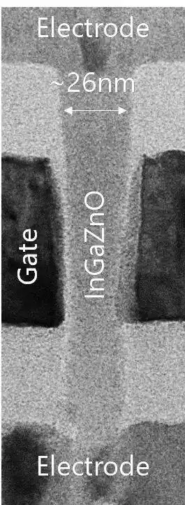
Cross-sectional TEM image of the InGaZnO vertical transistor

Due to its large bandgap and high electron mobility, InGaZnO transistors can theoretically achieve both ultra-low leakage and high on-current. KIOXIA, by optimizing contact electrode materials and spacer thickness, experimentally achieved over 15μA on-current while also realizing ultra-low leakage current below 10⁻¹⁸ A (as shown in the figure below). A significant portion of DRAM power consumption comes from refresh. Lower leakage leads to longer data retention time, reducing refresh pressure. Therefore, the core value of OCTRAM is using low-leakage oxide semiconductor transistors to reduce DRAM refresh power consumption.
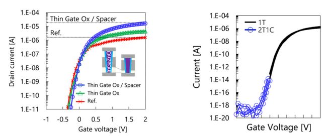
(a) On-current characteristics and (b) Off-current characteristics of the developed InGaZnO transistor

In September 2025, KIOXIA disclosed further reliability research on OCTRAM, focusing on TDDB lifetime issues of sub-25nm Gate-All-Around vertical InGaZnO transistors. TDDB stands for Time-Dependent Dielectric Breakdown. Simply put, it's whether the transistor's insulating layer gradually degrades and eventually fails under long-term electric field stress. KIOXIA stated they found lifetime degradation stems from two factors: intrinsic factors from scaling and extrinsic factors from the manufacturing process. By optimizing the process and reducing extrinsic degradation, KIOXIA achieved a projected TDDB lifetime exceeding 10 years.

In December 2025, KIOXIA announced progress closer to the core of 3D DRAM: developing oxide-semiconductor channel transistors capable of high stacking, having fabricated 8-layer horizontal transistor stacks with on-current exceeding 30μA and off-current below 1 aA, i.e., 10⁻¹⁸ A.

As of now, KIOXIA's 3D DRAM remains in the forefront R&D stage, not yet a commercial product.

KIOXIA is not a traditional DRAM giant, but its accumulated expertise in stacking processes, material integration, and array manufacturing from 3D NAND may give it an entry point in exploring next-generation 3D DRAM. Semiconductor Engineering also analyzed that KIOXIA's 3D DRAM path leverages mature oxide/nitride stacking capabilities from NAND to achieve lower-cost bit scaling, then uses IGZO to replace the channel to reduce thermal degradation issues.

However, one crucial point to emphasize is: KIOXIA's 3D DRAM is not HBM. HBM is packaging-level 3D; it stacks already manufactured DRAM dies to address high-bandwidth needs next to GPUs. KIOXIA's 3D DRAM is device/cell-level 3D; it aims to solve the problem of scaling the DRAM cell itself. Therefore, KIOXIA is not directly chasing HBM but is exploring a more fundamental 3D DRAM device path. If this path matures in the future, it may open a new technology branch for high-capacity, low-power working memory in the AI era.

Although 3D DRAM is still far from true commercialization. It currently resembles more of a future-facing technology ticket than an immediate revenue-contributing product line. But for KIOXIA, the significance of this ticket is not small. In the short term, KIOXIA can capitalize on the NAND recovery driven by AI; in the medium term, it advances high-layer BiCS FLASH; and in the long term, it bets on 3D DRAM, extending its 3D stacking capabilities from NAND to DRAM.

Conclusion

From massive losses and merger deadlock to the super myth of surpassing Toyota to become Japan's top-valued company in 2026, KIOXIA's rollercoaster trajectory is almost filled with the brutality and allure of the semiconductor memory industry. It was once cold-shouldered by capital markets for its single product line and missing the HBM wave, yet amid the tsunami of 'massive data flow' triggered by AI large models, it ushered in its own golden era by steadfastly adhering to NAND flash memory.

KIOXIA's comeback may not yet prove that Japanese semiconductors have truly revived. But at least it demonstrates one thing: in the semiconductor industry, a low point does not necessarily lead to exit. As long as technological assets remain, the realignment of cycles, capital, and demand can at any time bring a forgotten company back to the center of the table.

For KIOXIA, finding a long-term balance between fervent capital追捧 (pursuit) and the冷酷 (harsh) industry cycles moving forward will determine whether this lone sprout carrying the hopes of Japanese semiconductor revival is merely a fleeting flower in the AI supercycle or truly opens a new storage empire of its own.

*Disclaimer: This article was originally written by the author. The content represents the author's personal views. Semiconductor Industry Insights republishes it to convey a different perspective. This does not imply Semiconductor Industry Insights' agreement with or support for this view. If you have any objections, please contact Semiconductor Industry Insights.

Tiền kỹ thuật số thịnh hành

Câu hỏi Liên quan

QWhat triggered Kioxia's dramatic turnaround from a loss-making 'hot potato' to a stock market sensation in Japan?

AKioxia's dramatic turnaround was primarily triggered by the explosive demand for AI storage. The advent of large-scale AI models fundamentally shifted the market logic for memory. NAND flash, Kioxia's core product, became a scarce resource for AI inference, model storage, data lakes, enterprise SSDs, and nearline storage, leading to a supply shortage and surging profitability.

QWhat are the two key technologies (acronyms) introduced in Kioxia's 8th generation BiCS FLASH that significantly improved performance?

AThe two key technologies introduced in Kioxia's 8th generation BiCS FLASH are CBA (CMOS directly Bonded to Array) and OPS (On Pitch Select Gate). CBA improves density and speed by bonding separately optimized CMOS and array wafers, while OPS increases storage density by eliminating dummy areas within the memory array.

QWhat is the main technical advantage of Kioxia's OCTRAM (3D DRAM) technology over traditional DRAM?

AThe main technical advantage of Kioxia's OCTRAM technology is its use of InGaZnO (Oxide-Semiconductor) transistors, which offer extremely low leakage current (off-state current). This dramatically reduces refresh power consumption, a major challenge for traditional DRAM as it scales down, thereby enabling higher density and lower power 3D DRAM architectures.

QHow does Kioxia's approach to 3D DRAM (OCTRAM) fundamentally differ from High Bandwidth Memory (HBM)?

AKioxia's 3D DRAM (OCTRAM) is a device/cell-level 3D technology that aims to solve the fundamental scaling problems of the DRAM memory cell itself by stacking transistors vertically. In contrast, HBM is a package-level 3D technology that stacks pre-manufactured DRAM dies to achieve high bandwidth, primarily for GPU-adjacent memory. They address different layers of the memory hierarchy and scaling challenges.

QWhich major investors reaped enormous returns from Kioxia's stock surge, and what was the scale of one of their profits?

AThe major investors were Bain Capital (the parent company) and SK Hynix (an indirect major shareholder). Bain Capital's investment from the 2018 Toshiba Memory buyout became one of the most profitable private equity deals ever, with profits exceeding $15 billion and a return of nearly 20 times. The SK Hynix-led consortium is also expected to realize total profits far exceeding $70 billion.

Nội dung Liên quan

Vụ kiện 6,5 triệu USD của Polymarket có thể định hình lại tranh chấp thị trường dự đoán?

Hai nhà giao dịch của Polymarket, William Wood và Thomas Bush, đã kiện nền tảng thị trường dự đoán này vì vi phạm hợp đồng. Vụ tranh chấp liên quan đến thị trường dự đoán việc công ty Strategy có bán Bitcoin trước ngày 31/5 hay không. Theo đơn kiện, Wood và Bush nắm giữ cổ phần 'Có', đặt cược rằng Strategy sẽ bán BTC trong khung thời gian trên. Thực tế, công ty này đã xác nhận bán 32 BTC trong hồ sơ gửi Ủy ban Chứng khoán Mỹ (SEC) từ ngày 26 đến 31/5. Tuy nhiên, thay vì xác định kết quả thị trường là 'Có' dựa trên tiết lộ đó, Polymarket đã thêm ngôn ngữ "làm rõ" mới, hỏi lại liệu việc bán hàng có được xác nhận công khai trước ngày 31/5 hay không, và sau một cuộc bỏ phiếu xem xét cuối cùng bởi UMA, kết quả bị tuyên bố là 'Không'. Nguyên đơn cho rằng đây là hành vi vi phạm hợp đồng và thực hành lừa dối, gây thiệt hại tổng cộng 6,5 triệu USD cho 1.868 nhà giao dịch nắm giữ cổ phần 'Có'. Vụ kiện đã nhận chỉ trích từ giới nghiên cứu và có thể trở thành một trong những vụ kiện quan trọng nhất trong lĩnh vực thị trường dự đoán, với khả năng dẫn đến việc xem xét lại các thực hành giải quyết tranh chấp của UMA. Vụ việc diễn ra trong bối cảnh ngành này đang chịu sự giám sát ngày càng tăng và Ủy ban Giao dịch Hàng hóa Tương lai Mỹ (CFTC) đang xúc tiến một khuôn khổ pháp lý rõ ràng hơn.

ambcrypto15 phút trước

Vụ kiện 6,5 triệu USD của Polymarket có thể định hình lại tranh chấp thị trường dự đoán?

ambcrypto15 phút trước

Blockaid rút lại cảnh báo khai thác lỗ hổng cầu nối BTTC sau khi xác nhận hoạt động ngừng hoạt động

Công ty bảo mật blockchain Blockaid đã rút lại cảnh báo khai thác lỗ hổng liên quan đến Cầu BitTorrent Chain (BTTC) sau khi xác định rằng khoản rút 13,3 triệu USD tài sản là một phần của hoạt động nội bộ được ủy quyền, liên quan đến kế hoạch đóng cửa cầu của dự án. Sự việc diễn ra vào thứ Ba khi hệ thống giám sát của Blockaid phát hiện hoạt động trên chuỗi khả nghi, trông giống như một vụ xâm phạm cầu. Hoạt động bao gồm việc nâng cấp proxy đặc quyền và rút toàn bộ tài sản khỏi hợp đồng cầu, khiến Blockaid ban đầu phân loại đây là sự cố bảo mật tiềm ẩn. Tuy nhiên, ngay sau đó, Justin Sun, người sáng lập Tron, đã xác nhận rằng các giao dịch này là một phần của việc hoàn thành Chương trình Đóng cửa Cầu BTTC (BTTC Bridge Sunset Program). Ông khẳng định mọi quỹ của người dùng vẫn an toàn và việc gửi/rút tài sản đã qua cầu sẽ tiếp tục thông qua các sàn giao dịch tập trung đối tác. Thông báo này phù hợp với kế hoạch đã được BitTorrent công bố từ ngày 12 tháng 6 về việc đóng cửa cầu theo từng giai đoạn. Dự án cho biết họ sẽ chuyển trọng tâm sang các sáng kiến AI phi tập trung và duy trì giao thức phi tập trung BitTorrent.

ambcrypto24 phút trước

Blockaid rút lại cảnh báo khai thác lỗ hổng cầu nối BTTC sau khi xác nhận hoạt động ngừng hoạt động

ambcrypto24 phút trước

‘Chu kỳ thông thường’ bị gián đoạn? Hoskinson đổ lỗi chính trị Mỹ khiến tiền điện tử trì trệ

Charles Hoskinson, người sáng lập Cardano, đã chỉ trích sự can thiệp của chính trị Hoa Kỳ và đặc biệt là cựu Tổng thống Donald Trump vào thị trường tiền mã hóa. Ông cho rằng chu kỳ thị trường bình thường của crypto đã bị gián đoạn bởi sự bất ổn chính sách và sự phụ thuộc quá mức vào chính trị Mỹ, khiến các nhà đầu tư mất tập trung vào công nghệ và ứng dụng thực tế. Hoskinson tin rằng nếu không có yếu tố Mỹ, thị trường đã có một chu kỳ tăng trưởng thông thường và một mùa altcoin vào năm 2025. Ông cũng đề cập đến việc Trump công bố khoản thu nhập khổng lồ từ các dự án tiền mã hóa có liên quan đến gia đình, nhưng lo ngại rằng ngành công nghiệp này có thể bị "trừng phạt" thay vì các chính trị gia. Hoskinson so sánh giai đoạn hiện tại với "Gensler 2.0", cảnh báo về một đợt siết chặt quy định mới. Đồng quan điểm, Vitalik Buterin, nhà đồng sáng lập Ethereum, từng cảnh báo năm 2024 về việc không nên ủng hộ các ứng cử viên chính trị chỉ dựa trên lập trường "ủng hộ crypto", vì điều này tạo ra động cơ không lành mạnh. Bài viết kết thúc với thông tin về các rào cản pháp lý đối với kế hoạch dự trữ Bitcoin mà Trump đề xuất.

ambcrypto3 giờ trước

‘Chu kỳ thông thường’ bị gián đoạn? Hoskinson đổ lỗi chính trị Mỹ khiến tiền điện tử trì trệ

ambcrypto3 giờ trước

Giao dịch

Giao ngay

Bài viết Nổi bật

AGENT S là gì

Agent S: Tương Lai của Tương Tác Tự Động trong Web3 Giới thiệu Trong bối cảnh không ngừng phát triển của Web3 và tiền điện tử, các đổi mới đang liên tục định nghĩa lại cách mà cá nhân tương tác với các nền tảng kỹ thuật số. Một dự án tiên phong như vậy, Agent S, hứa hẹn sẽ cách mạng hóa tương tác giữa con người và máy tính thông qua khung tác nhân mở của nó. Bằng cách mở đường cho các tương tác tự động, Agent S nhằm đơn giản hóa các nhiệm vụ phức tạp, cung cấp các ứng dụng chuyển đổi trong trí tuệ nhân tạo (AI). Cuộc khám phá chi tiết này sẽ đi sâu vào những phức tạp của dự án, các tính năng độc đáo của nó và những tác động đối với lĩnh vực tiền điện tử. Agent S là gì? Agent S đứng vững như một khung tác nhân mở đột phá, được thiết kế đặc biệt để giải quyết ba thách thức cơ bản trong việc tự động hóa các nhiệm vụ máy tính: Thu thập Kiến thức Cụ thể theo Miền: Khung này học một cách thông minh từ nhiều nguồn kiến thức bên ngoài và kinh nghiệm nội bộ. Cách tiếp cận kép này giúp nó xây dựng một kho lưu trữ phong phú về kiến thức cụ thể theo miền, nâng cao hiệu suất của nó trong việc thực hiện nhiệm vụ. Lập Kế Hoạch Qua Các Tầm Nhìn Nhiệm Vụ Dài Hạn: Agent S sử dụng lập kế hoạch phân cấp tăng cường kinh nghiệm, một cách tiếp cận chiến lược giúp phân chia và thực hiện các nhiệm vụ phức tạp một cách hiệu quả. Tính năng này nâng cao đáng kể khả năng quản lý nhiều nhiệm vụ con một cách hiệu quả và hiệu suất. Xử Lý Các Giao Diện Động, Không Đều: Dự án giới thiệu Giao Diện Tác Nhân-Máy Tính (ACI), một giải pháp đổi mới giúp nâng cao tương tác giữa các tác nhân và người dùng. Sử dụng các Mô Hình Ngôn Ngữ Lớn Đa Phương Thức (MLLMs), Agent S có thể điều hướng và thao tác các giao diện người dùng đồ họa đa dạng một cách liền mạch. Thông qua những tính năng tiên phong này, Agent S cung cấp một khung vững chắc giải quyết các phức tạp liên quan đến việc tự động hóa tương tác giữa con người với máy móc, mở ra nhiều ứng dụng trong AI và hơn thế nữa. Ai là Người Tạo ra Agent S? Mặc dù khái niệm về Agent S là hoàn toàn đổi mới, thông tin cụ thể về người sáng lập vẫn còn mơ hồ. Người sáng lập hiện vẫn chưa được biết đến, điều này làm nổi bật giai đoạn sơ khai của dự án hoặc sự lựa chọn chiến lược để giữ kín các thành viên sáng lập. Bất chấp sự ẩn danh, sự chú ý vẫn tập trung vào khả năng và tiềm năng của khung này. Ai là Các Nhà Đầu Tư của Agent S? Vì Agent S còn tương đối mới trong hệ sinh thái mã hóa, thông tin chi tiết về các nhà đầu tư và những người tài trợ tài chính của nó không được ghi chép rõ ràng. Sự thiếu vắng thông tin công khai về các nền tảng đầu tư hoặc tổ chức hỗ trợ dự án dấy lên câu hỏi về cấu trúc tài trợ và lộ trình phát triển của nó. Hiểu biết về sự hỗ trợ là rất quan trọng để đánh giá tính bền vững và tác động tiềm năng của dự án. Agent S Hoạt Động Như Thế Nào? Tại cốt lõi của Agent S là công nghệ tiên tiến cho phép nó hoạt động hiệu quả trong nhiều bối cảnh khác nhau. Mô hình hoạt động của nó được xây dựng xung quanh một số tính năng chính: Tương Tác Giống Như Con Người: Khung này cung cấp lập kế hoạch AI tiên tiến, cố gắng làm cho các tương tác với máy tính trở nên trực quan hơn. Bằng cách bắt chước hành vi của con người trong việc thực hiện nhiệm vụ, nó hứa hẹn nâng cao trải nghiệm người dùng. Ký Ức Tường Thuật: Được sử dụng để tận dụng các trải nghiệm cấp cao, Agent S sử dụng ký ức tường thuật để theo dõi lịch sử nhiệm vụ, từ đó nâng cao quy trình ra quyết định của nó. Ký Ức Tình Huống: Tính năng này cung cấp cho người dùng hướng dẫn từng bước, cho phép khung này cung cấp hỗ trợ theo ngữ cảnh khi các nhiệm vụ diễn ra. Hỗ Trợ OpenACI: Với khả năng chạy cục bộ, Agent S cho phép người dùng duy trì quyền kiểm soát đối với các tương tác và quy trình làm việc của họ, phù hợp với tinh thần phi tập trung của Web3. Tích Hợp Dễ Dàng với Các API Bên Ngoài: Tính linh hoạt và khả năng tương thích với nhiều nền tảng AI khác nhau đảm bảo rằng Agent S có thể hòa nhập liền mạch vào các hệ sinh thái công nghệ hiện có, làm cho nó trở thành lựa chọn hấp dẫn cho các nhà phát triển và tổ chức. Những chức năng này cùng nhau góp phần vào vị trí độc đáo của Agent S trong không gian tiền điện tử, khi nó tự động hóa các nhiệm vụ phức tạp, nhiều bước với sự can thiệp tối thiểu của con người. Khi dự án phát triển, các ứng dụng tiềm năng của nó trong Web3 có thể định nghĩa lại cách mà các tương tác kỹ thuật số diễn ra. Thời Gian Phát Triển của Agent S Sự phát triển và các cột mốc của Agent S có thể được tóm tắt trong một dòng thời gian nêu bật các sự kiện quan trọng của nó: 27 tháng 9, 2024: Khái niệm về Agent S được ra mắt trong một bài nghiên cứu toàn diện mang tên “Một Khung Tác Nhân Mở Sử Dụng Máy Tính Như Một Con Người,” trình bày nền tảng cho dự án. 10 tháng 10, 2024: Bài nghiên cứu được công bố công khai trên arXiv, cung cấp một cái nhìn sâu sắc về khung và đánh giá hiệu suất của nó dựa trên tiêu chuẩn OSWorld. 12 tháng 10, 2024: Một video trình bày được phát hành, cung cấp cái nhìn trực quan về khả năng và tính năng của Agent S, thu hút thêm sự quan tâm từ người dùng và nhà đầu tư tiềm năng. Những dấu mốc trong dòng thời gian không chỉ minh họa sự tiến bộ của Agent S mà còn chỉ ra cam kết của nó đối với sự minh bạch và sự tham gia của cộng đồng. Những Điểm Chính Về Agent S Khi khung Agent S tiếp tục phát triển, một số thuộc tính chính nổi bật, nhấn mạnh tính đổi mới và tiềm năng của nó: Khung Đổi Mới: Được thiết kế để cung cấp cách sử dụng máy tính trực quan giống như tương tác của con người, Agent S mang đến một cách tiếp cận mới cho việc tự động hóa nhiệm vụ. Tương Tác Tự Động: Khả năng tương tác tự động với máy tính thông qua GUI đánh dấu một bước tiến tới các giải pháp tính toán thông minh và hiệu quả hơn. Tự Động Hóa Nhiệm Vụ Phức Tạp: Với phương pháp mạnh mẽ của nó, nó có thể tự động hóa các nhiệm vụ phức tạp, nhiều bước, làm cho các quy trình nhanh hơn và ít sai sót hơn. Cải Tiến Liên Tục: Các cơ chế học tập cho phép Agent S cải thiện từ các trải nghiệm trước đó, liên tục nâng cao hiệu suất và hiệu quả của nó. Tính Linh Hoạt: Khả năng thích ứng của nó trên các môi trường hoạt động khác nhau như OSWorld và WindowsAgentArena đảm bảo rằng nó có thể phục vụ một loạt các ứng dụng rộng rãi. Khi Agent S định vị mình trong bối cảnh Web3 và tiền điện tử, tiềm năng của nó để nâng cao khả năng tương tác và tự động hóa quy trình đánh dấu một bước tiến quan trọng trong công nghệ AI. Thông qua khung đổi mới của mình, Agent S minh họa cho tương lai của các tương tác kỹ thuật số, hứa hẹn một trải nghiệm liền mạch và hiệu quả hơn cho người dùng trên nhiều ngành công nghiệp khác nhau. Kết luận Agent S đại diện cho một bước nhảy vọt táo bạo trong sự kết hợp giữa AI và Web3, với khả năng định nghĩa lại cách chúng ta tương tác với công nghệ. Mặc dù vẫn còn ở giai đoạn đầu, những khả năng cho ứng dụng của nó là rộng lớn và hấp dẫn. Thông qua khung toàn diện của mình giải quyết các thách thức quan trọng, Agent S nhằm đưa các tương tác tự động lên hàng đầu trong trải nghiệm kỹ thuật số. Khi chúng ta tiến sâu hơn vào các lĩnh vực tiền điện tử và phi tập trung, các dự án như Agent S chắc chắn sẽ đóng một vai trò quan trọng trong việc định hình tương lai của công nghệ và sự hợp tác giữa con người với máy tính.

Tổng lượt xem 920Xuất bản vào 2025.01.14Cập nhật vào 2025.01.14

AGENT S là gì

Làm thế nào để Mua S

Chào mừng bạn đến với HTX.com! Chúng tôi đã làm cho mua Sonic (S) trở nên đơn giản và thuận tiện. Làm theo hướng dẫn từng bước của chúng tôi để bắt đầu hành trình tiền kỹ thuật số của bạn.Bước 1: Tạo Tài khoản HTX của BạnSử dụng email hoặc số điện thoại của bạn để đăng ký tài khoản miễn phí trên HTX. Trải nghiệm hành trình đăng ký không rắc rối và mở khóa tất cả tính năng. Nhận Tài khoản của tôiBước 2: Truy cập Mua Crypto và Chọn Phương thức Thanh toán của BạnThẻ Tín dụng/Ghi nợ: Sử dụng Visa hoặc Mastercard của bạn để mua Sonic (S) ngay lập tức.Số dư: Sử dụng tiền từ số dư tài khoản HTX của bạn để giao dịch liền mạch.Bên thứ ba: Chúng tôi đã thêm những phương thức thanh toán phổ biến như Google Pay và Apple Pay để nâng cao sự tiện lợi.P2P: Giao dịch trực tiếp với người dùng khác trên HTX.Thị trường mua bán phi tập trung (OTC): Chúng tôi cung cấp những dịch vụ được thiết kế riêng và tỷ giá hối đoái cạnh tranh cho nhà giao dịch.Bước 3: Lưu trữ Sonic (S) của BạnSau khi mua Sonic (S), lưu trữ trong tài khoản HTX của bạn. Ngoài ra, bạn có thể gửi đi nơi khác qua chuyển khoản blockchain hoặc sử dụng để giao dịch những tiền kỹ thuật số khác.Bước 4: Giao dịch Sonic (S)Giao dịch Sonic (S) dễ dàng trên thị trường giao ngay của HTX. Chỉ cần truy cập vào tài khoản của bạn, chọn cặp giao dịch, thực hiện giao dịch và theo dõi trong thời gian thực. Chúng tôi cung cấp trải nghiệm thân thiện với người dùng cho cả người mới bắt đầu và người giao dịch dày dạn kinh nghiệm.

Tổng lượt xem 1.7kXuất bản vào 2025.01.15Cập nhật vào 2026.06.02

Làm thế nào để Mua S

Thảo luận

Chào mừng đến với Cộng đồng HTX. Tại đây, bạn có thể được thông báo về những phát triển nền tảng mới nhất và có quyền truy cập vào thông tin chuyên sâu về thị trường. Ý kiến ​​của người dùng về giá của S (S) được trình bày dưới đây.

活动图片