# Сопутствующие статьи по теме Chip Design

Новостной центр HTX предлагает последние статьи и углубленный анализ по "Chip Design", охватывающие рыночные тренды, новости проектов, развитие технологий и политику регулирования в криптоиндустрии.
Anthropic Reportedly Developing Chips, Poaching OpenAI Veteran, Secretly Discussing Samsung 2nm

Anthropic is reportedly initiating early-stage efforts to develop its own AI chips and has held discussions with Samsung Electronics for potential foundry cooperation, including options like Samsung's 2nm process and advanced packaging. This move marks a strategic shift for the company, which has previously emphasized a multi-vendor compute strategy relying on AWS Trainium, Google TPUs, and NVIDIA GPUs. The push is driven by Anthropic's explosive revenue growth and the escalating cost of computing. Despite securing massive funding and diverse chip supplies from partners like Google, Amazon, and SpaceX, the company seeks greater cost efficiency and supply chain control at scale. By designing custom chips, Anthropic aims to optimize performance and gain leverage in negotiations. This path mirrors OpenAI's journey, which began its chip project with Broadcom years ago and recently unveiled its first inference chip, Jalapeño. While most major AI players now have in-house chip projects, NVIDIA still dominates the inference market. Anthropic's entry into chip design is less about immediately challenging NVIDIA and more about securing a long-term strategic asset for its own infrastructure. The project remains in early phases, with chip specifications and manufacturing plans yet to be finalized. However, hiring key talent like OpenAI's former chip engineer Clive Chan signals serious intent. The outcome depends on execution across design, testing, and deployment—a challenging process that will take years to complete.

marsbit07/03 07:55

Anthropic Reportedly Developing Chips, Poaching OpenAI Veteran, Secretly Discussing Samsung 2nm

marsbit07/03 07:55

Huawei's "Tao Law": A Comprehensive Overview of Core Companies

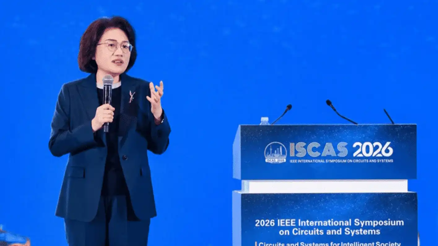
Huawei's "Tau Law": Core Companies Overview On May 25, 2026, Huawei's Director and President of the Semiconductor Business Division, He Tingbo, formally introduced the "Tau (τ) Law" at ISCAS 2026, marking a significant principle guiding industry development in the global semiconductor field from China. The Tau Law shifts focus from traditional Moore's Law, which pursues geometric transistor scaling, to "time scaling"—continuously compressing signal propagation delay (time constant τ) without solely relying on extreme feature size reduction. The core implementation path is "logic folding." This technique transforms circuit layouts from two-dimensional planes to multi-layer 3D stacks, using short vertical interconnects to replace long horizontal wiring, thereby drastically reducing τ. Huawei has already designed and mass-produced 381 chips following this principle over the past six years, with plans to launch a Kirin chip utilizing logic folding in Fall 2026. By 2031, high-end chips based on the Tau Law are expected to achieve performance levels equivalent to a 1.4nm process node. This development impacts several key industry segments, with related Chinese companies poised to benefit: 1. **EDA Design Software**: Essential for circuit-level optimization. Key players include: * **Empyrean Technology** (Huada Jiutian): China's largest full-flow EDA provider. * **Primarius Technologies** (Gailun Dianzi): Specializes in device modeling and verification. * **Semitronix** (Guangliwei): Focuses on yield enhancement and test chip EDA. 2. **Chiplet & Advanced Packaging**: Logic folding's 3D stacking necessitates advanced packaging (e.g., TSV, hybrid bonding). Core participants are: * **Tongfu Microelectronics**: A leader in advanced packaging and a key partner for AMD's Chiplet products. * **JCET Group** (Changdian Keji) & **Tianshui Huatian Technology**: Major OSATs with advanced packaging capabilities. * **VeriSilicon** (Xinyuan Gufen): Provides Chiplet-based design platforms and IP. 3. **Foundry Manufacturing**: Optimization must be implemented in transistor structures and process parameters. Potential foundries for Huawei's future chips include: * **SMIC**: China's leading foundry with advanced FinFET capabilities, the most likely candidate for next-gen Kirin chips. * **Hua Hong Semiconductor** (Huahong Gongsi): A leader in specialty processes (power, embedded memory). * **Nexchip Semiconductor** (Jinghe Jicheng): Major foundry for display driver ICs and MCUs. The Tau Law represents a strategic move towards architectural innovation and design-process co-optimization, driving demand across the domestic semiconductor supply chain.

marsbit05/25 11:33

Huawei's "Tao Law": A Comprehensive Overview of Core Companies

marsbit05/25 11:33

活动图片