Glass Substrate Suddenly Accelerates

marsbitОпубликовано 2026-06-25Обновлено 2026-06-25

Введение

The adoption of glass substrates in the semiconductor industry is accelerating unexpectedly. Following collaboration announcements between BOE and Corning in late May, and earlier moves by Intel and TSMC, the market for related upstream companies has surged. Intel's "Glass Core Substrate" aims to replace the IC substrate between the circuit board and the chip, primarily addressing thermal warping issues in large AI chips. TSMC's focus is on replacing the expensive silicon interposer layer within the chip package to significantly reduce costs. While initially cautious, with timelines stretching towards 2030, progress has been dramatically pulled forward. Key drivers are NVIDIA, whose ever-larger GPUs like the upcoming Rubin make glass substrates a necessity, and the display panel industry. Companies like Innolux and BOE, leveraging their extensive experience and production lines in panel-grade glass substrates, are rapidly retooling for semiconductor packaging. Innolux has already established production lines and secured orders, while BOE has built pilot lines and is sampling customers. Although technical hurdles remain, such as advanced multi-layer glass processing and copper electroplating, the path to commercialization is now clearer. Large-scale adoption is estimated to begin by late 2027, marking glass substrates as a critical next step in supporting advancing AI computing power.

The AI computing power market is advancing in waves, with gains moving from one segment to another, and now it's the turn of glass substrates.

In late May, BOE announced a memorandum of cooperation with Corning on glass substrates, completely igniting the market.

Not only did its own steady stock price suddenly spike "like a jolt from a heartbeat monitor," with two consecutive trading days of limit-up gains, but upstream companies like Rainbow Display and Wufang Optoelectronics also hit the daily limit-up, Dier Laser's stock price reached a record high, and Vogo Optoelectronics has surged nearly 300% over the past two months.

Institutions have identified 2026 as the first year for commercial validation of glass substrates. Besides the cooperation between BOE and Corning, Intel announced successful mass production of glass core substrates in its latest server CPUs, and TSMC revealed the establishment of a glass substrate CoPoS packaging trial production line.

The two giants are pushing hard, setting the stage perfectly for the bullish atmosphere.

It must be said that the commercialization speed of glass substrates has already exceeded most people's expectations.

Replacing the "Board" in Chips

Intel and TSMC are the current top promoters of glass substrates, but the "glass substrates" they refer to are not exactly the same thing.

A chip is composed of various components mounted on carrier substrates, forming functional units. These functional units are then mounted on the next layer of carrier substrate, creating a larger functional unit, and so on, presenting a hierarchical structure.

For example, the most familiar circuit board is the bottom-most carrier substrate. Further up, there are core substrates, IC substrates, and so on.
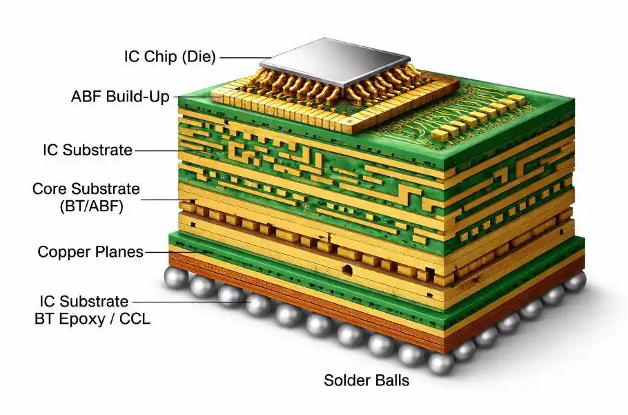
Different layers of "boards" inside a chip; Image source: IC Components

These carrier substrates were traditionally mostly made of materials like resin, fiberglass, copper foil, silicon, etc. As the name suggests, a glass substrate uses glass as the primary material for the substrate.

What Intel and TSMC aim to do is replace mainstream carrier substrates with glass substrates, but they are not targeting the same "board."

Intel's "advanced packaging glass substrate," officially named "Glass Core Substrate," replaces the IC substrate layer between the circuit board and the chip.
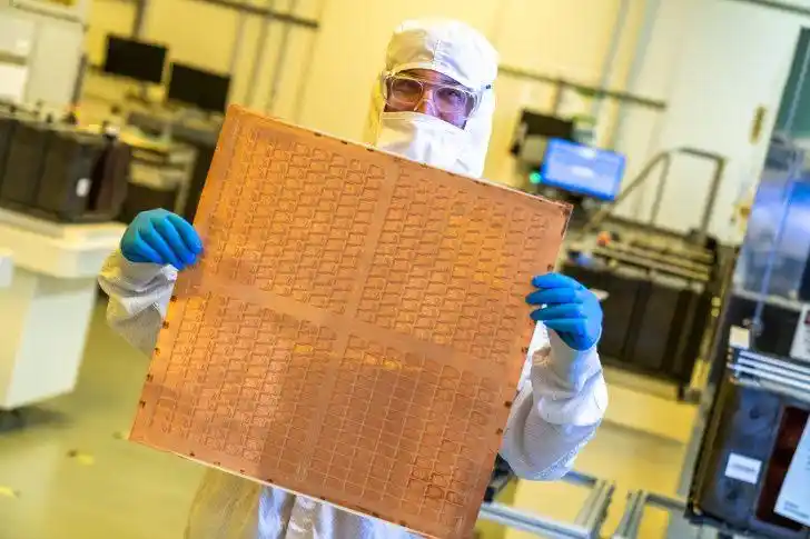
A test glass core substrate displayed by Intel

Currently, mainstream AI chips, including Nvidia GPUs, use substrates primarily made of ABF material. The biggest drawback is their tendency to warp and deform when heated. A one-meter-long ABF carrier substrate expands about 15 micrometers for every 1°C increase in temperature.

In contrast, the silicon chip placed on top of the ABF substrate shows almost no deformation when heated.

Thus, when heat is generated during chip operation, the bottom ABF substrate expands outward due to heat, while the upper silicon chip remains unchanged, causing the entire substrate to bend or "warp."

The larger the chip size, the more severe the warping becomes—imagine a credit card with all four corners curling up simultaneously. The consequences could be catastrophic.
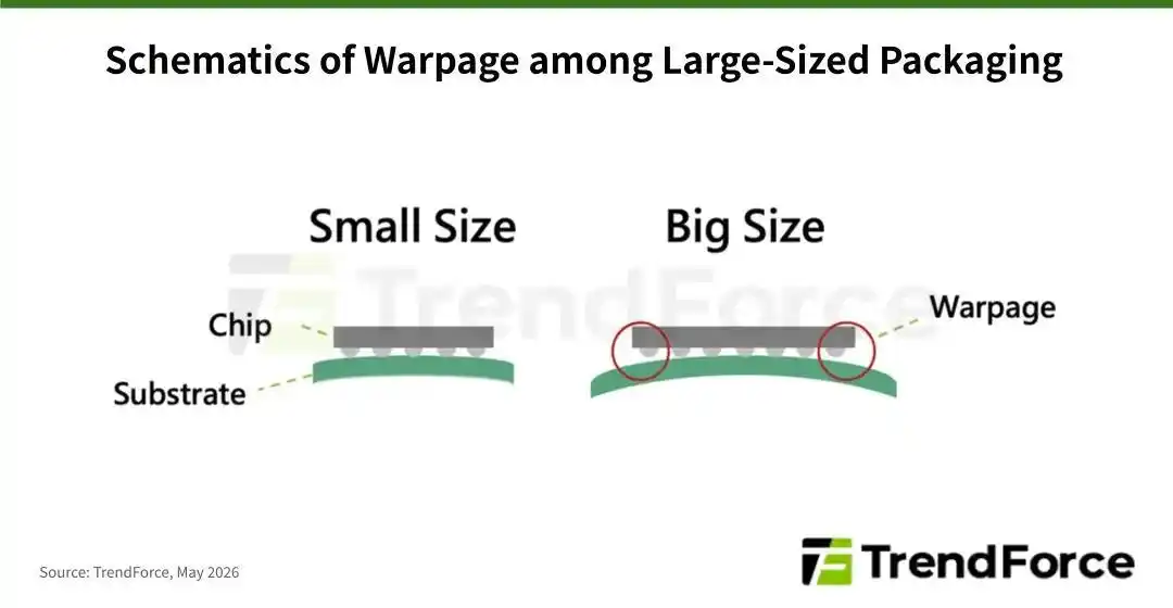
The larger the carrier substrate size, the more obvious the warping; Image source: TrendForce

This is why glass substrates are being considered. Due to their "heat resistance" being comparable to silicon chips, even if they deform at high temperatures, they can maintain synchronization with the silicon chip, effectively preventing warping.

Compared to Intel, TSMC wants to replace a carrier substrate located one layer higher—the bare die layer of the chip.

A GPU bare die consists of computing core units (CPU/GPU) and multiple HBM stacks, placed on a silicon interposer. This silicon interposer is the "board" TSMC most wants to replace.
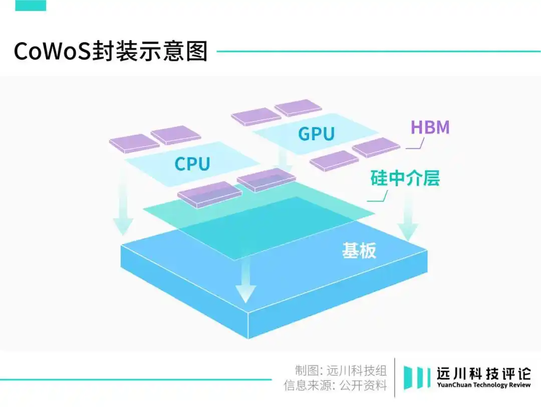
The manufacturing cost of a silicon interposer is extremely high, with a unit price exceeding $100 for a large-size silicon interposer [2]. For comparison, the A19 Pro chip in the iPhone 17 Pro Max costs only about $90 per unit for procurement.

Moreover, compared to these powerful computing SoCs for phones, the silicon interposer's main function is merely data transfer, akin to buying a scooter for the price of a sports car, which sounds even worse.

The size of the silicon interposer is directly related to the size of the AI chip and the number of HBM stacks used. As AI chips become larger and more HBM is used, the cost sinkhole for silicon interposers deepens.

For companies purchasing AI chips, it's like buying a car for $100,000 and having to spend an additional $50,000 on a license plate to drive it.

Replacing the silicon interposer with a glass substrate offers the biggest advantage: cost. For the same size, it costs less than half of the silicon counterpart [2].

The ideas from Intel and TSMC are both reasonable, but the implementation of new technology is never a simple order. Especially in the chip industry, new technology challenges not just the laws of physics.

Chip manufacturing is humanity's most complex activity to date, having solidified over the past half-century into an extremely strict set of rules. The upstream and downstream segments have meticulously built a standardized system where everything is tightly interlocked; a small adjustment can affect everything.

Even the slightest adjustment may lead to changes or complete overhauls in upstream equipment and materials.

Hence, while giants talk boldly about innovation, their actions remain conservative and cautious.

Intel proposed the glass core substrate concept in 2023, with mass production vaguely scheduled for sometime between 2026 and 2030. TSMC has been secretive about its CoPoS plan, only recently revealing for the first time that it would take 2-3 years to scale up to a certain size.

However, a few big hands have forcefully yanked the progress bar forward by a large margin.

Who is Pulling the Progress Bar?

The first big hand is Nvidia.

Just a few months after Intel announced the glass core substrate, Morgan Stanley released a report predicting that GB200 "might" use glass substrates for packaging.

This report was once overinterpreted as "Nvidia officially announced GB200 will use glass substrates," causing another surge in related concept stocks.

Putting the misunderstanding aside, the fact that an unsupported speculation could have such strong persuasive power is because, in the public's perception, Nvidia indeed has the greatest motivation to push glass substrate adoption.

Nine out of ten AI computing power chips are Nvidia GPUs. Bearing the weight of exponentially increasing computing demands, each GPU generation strives to pack more transistors, leading to larger and larger GPUs.

The B200's area is nearly double that of its predecessor, the H100, almost 10 times the size of Apple's M2 Ultra chip, roughly half the size of a bank card, already pushing the warping limits of ordinary IC substrates.

The upcoming Rubin, set for mass production in the second half of the year, is even larger than the B200. Changing materials is not an option but a necessity.
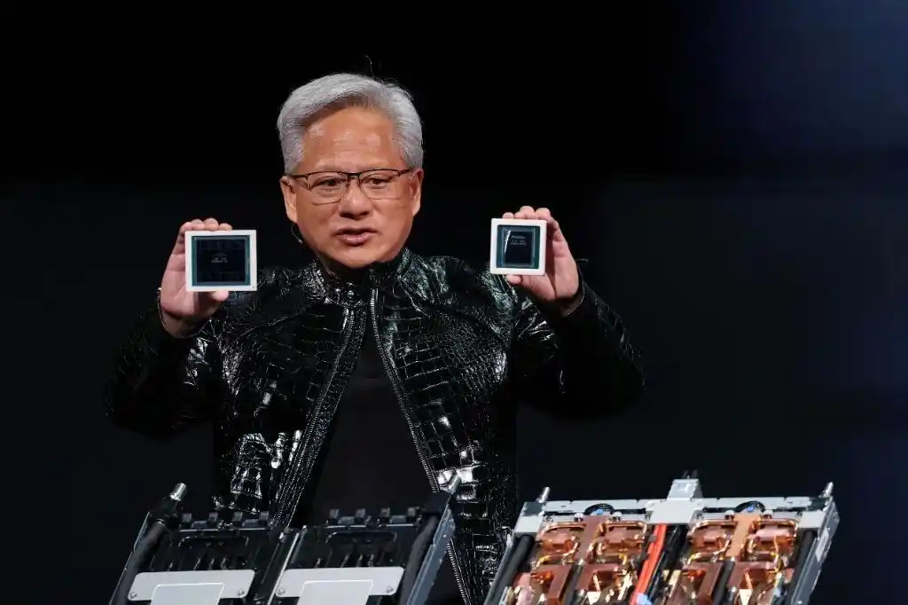
Jensen Huang holding B200 (left) and H100 (right)

In March this year, Nvidia announced a full shift to glass substrates, with Rubin leading the trial, fast-forwarding the commercialization timeline to the end of this year.

With Nvidia's big hand pulling from the front, an unexpected big hand is pushing from behind. It's not from the upstream chip industry, but from a neighboring sibling industry—display panels.

Before being used in chip packaging, the largest downstream application for glass substrates was display panels.

A display panel has a sandwich structure internally, with the two "slices of bread" being glass substrates—one controlling brightness, the other controlling color.
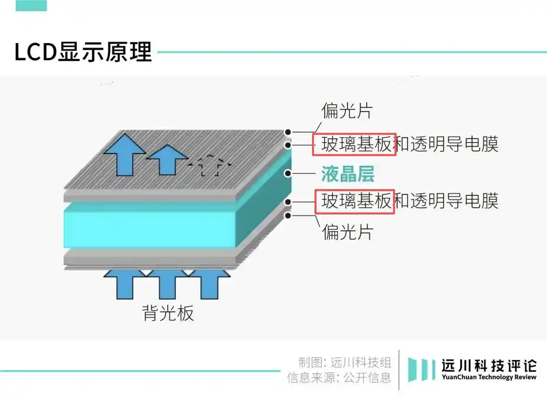
Glass substrates in an LCD panel

The precision processing technologies and equipment used here have extremely high overlap with those needed for glass substrates in chips. Exaggerating a bit, high-end production lines can be modified for use.

Therefore, regarding glass substrate implementation, the most enthusiastic are actually brothers from the panel industry.

For example, Taiwan's major panel maker Innolux plotted a transition to chip packaging as early as 2019.

With a global panel price war raging fiercely, Innolux, seeing it couldn't hold out, accepted an olive branch from Taiwan's Industrial Technology Research Institute (ITRI) to jointly develop glass substrate-based chip packaging technology, modifying its own panel production lines.

By the time Intel announced glass substrate technology in 2023, Innolux had already built the world's first FOPLP packaging production line converted from a panel line.

The following year, it secured major orders from chip giants NXP and STMicroelectronics, and sold an idle 5.5-generation panel line at a high price to TSMC to alleviate the latter's shortage of advanced packaging capacity.

By early this year, Innolux's FOPLP advanced packaging line had increased monthly production tenfold to tens of millions, not only firmly embracing TSMC's leg but reportedly also entering SpaceX's Starlink supply chain.

Taiwan's panel makers work fiercely hard, and progress on the mainland side is equally rapid.

BOE began researching and developing glass substrates in 2020, invested nearly 1 billion yuan in building a pilot line in 2024, and achieved fully automated equipment operation in the first half of this year [4].

It has already started sending samples to customers for testing and validation. The cooperation with Corning in May was to lock in future years of upstream specialty glass supply, with large-scale mass production imminent.

Mainland China holds over 60% of global panel capacity, especially in high-generation panels with the world's most mature and highly automated production lines. A bigger advantage lies in having a complete upstream industry chain for support.

Several companies currently of most interest in the secondary market, such as Dier Laser, Han's Laser, and Delong Laser, are upstream manufacturers of TGV (Through Glass Via) laser microvia equipment. Vogo Optoelectronics is midstream, handling glass substrate processing.

Beyond Chinese manufacturers, Korea's Samsung Electro-Mechanics, LG Innotek, Japan's Dainippon Printing, and Nippon Electric Glass are all active proponents of glass substrates—familiar faces from the panel wars.

With downstream demand secured by big spenders and upstream sibling industries providing warm support, glass substrates have quickly progressed from being seriously criticized as "concept hype" to the "eve of mass production." Securities firms have changed their cautious stance, drawing bigger and bigger pies.

Objectively speaking, there are still several technical hurdles to overcome before glass substrates achieve large-scale implementation.

For example, the core material—specialty glass—currently only Corning can process up to 11 layers without cracking, while the domestic supply chain can manage at most 3-4 layers [5]. Other issues include insufficient copper electroplating equipment and processes [5].

According to industry chain estimates, the earliest large-scale volume production for glass substrates will likely be by the end of 2027.

The end of computing power is electricity, but before reaching that end, the industry chain must cross another hurdle—perhaps one more glass substrate.

References

[1] Research on Warpage of 2.5D CoWoS Packaging Based on Glass Substrate, Shi Hangbo, Wang Xu, Fan Jilei, et al.

[2] Large Silicon Interposer Unit Price Exceeds $100, Accounting for Half the Cost; How Can AI Computing Chips Break Through the Packaging Cost Bottleneck? Yue Tou Gu

[3] Complete Breakdown of TGV Glass Via: After Intel's Glass Substrate Entry, Understanding the Hard Barriers, 2027 Mass Production Countdown, and Taiwan Supply Chain Investment Map, Sinopac Securities

[4] BOE: Glass Substrate Packaging Carrier Pilot Line Operational, Design Capacity 1000 Sheets/Month, Future Semiconductor

[5] Glass Substrate Industry Exchange, Summary Research Report

This article is from the WeChat public account "Yuanchuan Technology Review" (ID: kechuangych), author: He Lüheng, editor: Li Motian

Трендовые криптовалюты

Связанные с этим вопросы

QWhat are the two main applications of glass substrates in the chip industry, as promoted by Intel and TSMC respectively?

AIntel promotes the use of 'Glass Core Substrate' to replace the IC substrate layer (between the circuit board and the chip). TSMC aims to use glass substrates to replace the silicon interposer layer (within the chip's bare die layer).

QWhy is the transition to glass substrates becoming increasingly necessary for high-performance AI chips like NVIDIA's GPUs?

AAs AI GPUs become larger (e.g., B200, Rubin) to pack more transistors, the traditional organic ABF substrates are prone to warping due to heat. Glass substrates have thermal properties similar to silicon, preventing this warping and enabling larger chip designs.

QWhich non-semiconductor industry is playing a significant role in accelerating the adoption of glass substrates for chip packaging, and why?

AThe display panel industry is a key accelerator. Companies like Innolux and BOE are repurposing their mature, high-precision panel manufacturing lines and expertise for glass substrate processing, providing ready-made production capacity and supply chain support.

QWhat is the primary benefit for TSMC in replacing silicon interposers with glass substrates in its CoWoS packaging?

AThe primary benefit is significant cost reduction. Large silicon interposers are extremely expensive (over $100 each), while similarly sized glass substrates are estimated to cost less than half that amount.

QAccording to the article, what are some of the key technical challenges that still need to be overcome before glass substrates can achieve mass adoption?

AKey challenges include: 1) Developing special glass materials that can withstand multiple layers (e.g., 11+) of processing without breaking; 2) Improving copper electroplating equipment and processes for creating high-quality interconnects within the glass substrate.

Похожее

Диалог с сооснователем Hyperdash: Почему Hyperliquid все еще сильно недооценен?

Источник: The Rollup Сооснователь и CRO платформы анализа данных Hyperdash, Hanson Birringer, в подкасте The Rollup объяснил, почему Hyperliquid остается недооцененным. Он выделил три ключевых тренда, на которых строится экосистема: децентрализованные бессрочные фьючерсы (перпеты), токенизированные реальные активы (RWA) и стейблкоины. Hyperliquid — это децентрализованная платформа, которая объединяет высокую производительность, необходимую институциональным инвесторам, с открытостью и разрешениями криптовалютного пространства. Платформа уже является лидером среди DEX по объему открытого интереса и торговли перпетами, включая новые рынки, такие как товары и акции. Важным шагом стало внедрение USDC в качестве основного расчётного актива, что создает новую модель получения дохода. Часть доходов от стейблкоинов (которые размещаются в низкорисковые активы, например, казначейские облигации США) направляется в фонд для выкупа и сжигания собственного токена HYPE, создавая постоянный покупательский спрос. Для привлечения традиционных институциональных капиталов был создан фонд Hyper Holdings, который выступил посевным инвестором для ETF на Hyperliquid от Grayscale. Это дает институциям удобный и регулируемый доступ к экосистеме. Несмотря на текущие регуляторные сложности для прямого подключения традиционных брокерских платформ, команда активно работает с регуляторами, чтобы создать чёткие правила для децентрализованных торговых площадок. Приобретение Hyperdash компании Imperator укрепило инфраструктуру данных и нод, улучшив инструменты как для розничных, так и для институциональных трейдеров. По мнению Беррингера, основной бычий сценарий для Hyperliquid связан с глобальной финансовой инклюзией — предоставлением доступа к ликвидности миллиардам людей через смартфон. Медвежий сценарий, который мог бы остановить этот рост, маловероятен, так как соответствует долгосрочным трендам цифровизации и открытости финансов.

marsbit1 ч. назад

Диалог с сооснователем Hyperdash: Почему Hyperliquid все еще сильно недооценен?

marsbit1 ч. назад

Обнародована «полнокровная» версия DeepSeek V4, релиз, возможно, уже завтра

Весь Интернет ждал почти три месяца! Официальный релиз DeepSeek V4 ожидается уже завтра или в ближайшие дни. Некоторые пользователи уже получили доступ к предварительному тестированию. Будут выпущены две версии: DeepSeek V4 Flash и DeepSeek V4 Pro. По предварительным оценкам, общая производительность модели находится на уровне Opus 4.8, способности в области программирования сравнимы с GPT-5.6 Sol, а возможности Agent, генерации 3D и SVG значительно улучшились. Хотя, вероятно, она не превзойдёт недавно выпущенный Kimi K3, её цена будет заметно ниже. В первых демонстрациях уже видны возможности V4: создание 3D-игр, HTML-игр в стиле смеси Minecraft и No Man’s Sky, классической игры Cut the Rope и т.д. Важнейшим фактором станет цена. DeepSeek внедрит «пиковое ценообразование» для API. Стоимость миллиона выходных токенов для deepseek-v4-pro составит $0,87 в обычное время и $1,74 в пиковый период; для deepseek-v4-flash — $0,28 и $0,56 соответственно, при этом цена за кэшированные входные токены остаётся крайне низкой. По сравнению с Fable 5 ($50 за миллион выходных токенов), V4 сохраняет огромное преимущество в соотношении цены и производительности. Это следует проверенной стратегии DeepSeek: предложить возможности уровня Opus по значительно более низкой цене. С 24 июля модели deepseek-chat и deepseek-reasoner будут сняты с эксплуатации. Ожидается, что DeepSeek V4, сочетая высокую производительность и привлекательную стоимость, вновь создаст «момент DeepSeek» на рынке.

marsbit1 ч. назад

Обнародована «полнокровная» версия DeepSeek V4, релиз, возможно, уже завтра

marsbit1 ч. назад

WEEX Labs Еженедельный обзор: «Перераспределение власти» в инфраструктуре ИИ и «глубокое погружение» в реальную экономику

Июль 2026 года ознаменовал ключевой поворот в индустрии ИИ: **переход права распределения вычислительных мощностей от «облачных гигантов» к «владельцам вычислений» и смещение ценностного ориентира ИИ от «гонки параметров» к «интеграции в реальный сектор»**. Основные изменения недели: * **Реорганизация облака вычислений**: Meta анонсировала услугу «MetaCompute», бросая вызов традиционным провайдерам (AWS, Azure). Это усиливает конкуренцию и делает «экосистему больших моделей» ключевым фактором выбора для предприятий. * **Прорыв китайских моделей**: Открытый исходный код и запуск моделей (DeepSeek-V4, Tencent Hunyuan Hy-3) указывают на этап «коммунальности». Конкуренция смещается в сторону экстремального соотношения цены и качества, снижая порог входа. * **Воплощенный ИИ на практике**: Политика стимулирует переход человекоподобных роботов из лабораторий в реальные производственные условия (логистика, автомобилестроение). Ценность измеряется стабильностью данных и реальной эффективностью на фабрике. * **Глобальное управление**: Концепция «суверенного ИИ» становится практической основой для национальных стратегий, устанавливая более высокие барьеры соответствия и требования к архитектуре моделей. **Итог**: Процветание ИИ переходит от виртуального мира к интеграции в глобальную производственную ткань. Рекомендации для компаний: 1. Использовать открытые модели (например, DeepSeek) для создания частных корпоративных решений. 2. Избегать «блокировки поставщика» вычислительных мощностей, сохраняя разнообразие. 3. Искать возможности в инфраструктуре для воплощенного ИИ (сбор данных, промышленное ПО, сервисы адаптации), а не только в создании роботов.

marsbit1 ч. назад

WEEX Labs Еженедельный обзор: «Перераспределение власти» в инфраструктуре ИИ и «глубокое погружение» в реальную экономику

marsbit1 ч. назад

Надежен ли WEEX TradFi? Что вам следует знать перед первой торговлей токенизированными акциями США

В последние годы пользователи крипторынка все чаще обращают внимание на традиционные финансовые активы, такие как акции ведущих компаний (Nvidia, Apple и др.), индексы и товары. Это стирает границы между криптовалютными и традиционными рынками. Такие платформы, как WEEX TradFi, предлагают токенизированные версии этих активов (токены акций), позволяя торговать ими в привычной цифровой среде. Важно понимать, что торговля токенами акций (например, токеном NVDA) — это не то же самое, что владение реальными акциями. Пользователи получают доступ к ценовым движениям базового актива, но не становятся акционерами с правом голоса или получения дивидендов. Преимуществом является знакомый интерфейс и возможность торговли 24/7, в отличие от традиционных бирж с фиксированными часами работы. Перед началом торговли необходимо оценить надежность продукта: понять его механизм, как отслеживается цена базового актива, а также осознавать связанные риски. Традиционные активы также подвержены волатильности из-за корпоративных новостей, макроэкономических факторов и изменений ликвидности в нерабочее время основных бирж. Таким образом, TradFi становится новым мостом, соединяющим мир криптовалют с глобальными финансовыми рынками. Для пользователей ключевое значение имеют прозрачность правил торговли, управление рисками и четкое понимание того, чем они торгуют. Надежность платформы определяется не только ассортиментом активов, но и способностью пользователя ответственно подходить к торговле в этой новой, расширенной среде.

marsbit1 ч. назад

Надежен ли WEEX TradFi? Что вам следует знать перед первой торговлей токенизированными акциями США

marsbit1 ч. назад

Coinbase «немного отдалилась от пользователей», утверждает Cobie — Есть ли решение?

Известный криптоинфлюэнсер Rune спросил Джордана Фиша (Cobie), как он планирует увеличить использование приложения Base, учитывая, что руководство Base подорвало доверие криптосообщества. Фиш, отвечающий за торговые продукты Coinbase и недавно возглавивший Base App, признал, что Coinbase находилась в «башне из слоновой кости» и была дистанцирована от пользователей, особенно от криптоэнтузиастов. Его цель — сблизить разработчиков и пользователей, лучше представлять интересы ончейн-сообщества и создавать продукты, которые людям действительно нравятся. Ситуация усугубилась инцидентом с генеральным директором Coinbase Брайаном Армстронгом, который использовал в качестве аватара CryptoPunk, которым не владел. После критики он сменил аватар на мем с собой, что спровоцировало создание мемкоина «Brian» на Base, чья капитализация быстро достигла $20 млн. После покупки настоящего CryptoPunk за $200 000 и смены аватара интерес к мемкоину угас, и его стоимость рухнула. В итоге, Jordan Fish признает необходимость восстановления доверия, а инцидент с Армстронгом добавил напряженности в и без того сложную ситуацию вокруг Coinbase и Base.

ambcrypto1 ч. назад

Coinbase «немного отдалилась от пользователей», утверждает Cobie — Есть ли решение?

ambcrypto1 ч. назад

Торговля

Спот

Популярные статьи

Как купить WAVES

Добро пожаловать на HTX.com! Мы сделали приобретение Waves (WAVES) простым и удобным. Следуйте нашему пошаговому руководству и отправляйтесь в свое крипто-путешествие.Шаг 1: Создайте аккаунт на HTXИспользуйте свой адрес электронной почты или номер телефона, чтобы зарегистрироваться и бесплатно создать аккаунт на HTX. Пройдите удобную регистрацию и откройте для себя весь функционал.Создать аккаунтШаг 2: Перейдите в Купить криптовалюту и выберите свой способ оплатыКредитная/Дебетовая Карта: Используйте свою карту Visa или Mastercard для мгновенной покупки Waves (WAVES).Баланс: Используйте средства с баланса вашего аккаунта HTX для простой торговли.Третьи Лица: Мы добавили популярные способы оплаты, такие как Google Pay и Apple Pay, для повышения удобства.P2P: Торгуйте напрямую с другими пользователями на HTX.Внебиржевая Торговля (OTC): Мы предлагаем индивидуальные услуги и конкурентоспособные обменные курсы для трейдеров.Шаг 3: Хранение Waves (WAVES)После приобретения вами Waves (WAVES) храните их в своем аккаунте на HTX. В качестве альтернативы вы можете отправить их куда-либо с помощью перевода в блокчейне или использовать для торговли с другими криптовалютами.Шаг 4: Торговля Waves (WAVES)С легкостью торгуйте Waves (WAVES) на спотовом рынке HTX. Просто зайдите в свой аккаунт, выберите торговую пару, совершайте сделки и следите за ними в режиме реального времени. Мы предлагаем удобный интерфейс как для начинающих, так и для опытных трейдеров.

623 просмотров всегоОпубликовано 2024.03.29Обновлено 2026.06.02

Как купить WAVES

Обсуждения

Добро пожаловать в Сообщество HTX. Здесь вы сможете быть в курсе последних новостей о развитии платформы и получить доступ к профессиональной аналитической информации о рынке. Мнения пользователей о цене на WAVES (WAVES) представлены ниже.

活动图片