18 Bulan Naik Lebih dari 50 Kali Lipat, Kioxia Melakukan Kebangkitan Epik

marsbitPublished on 2026-06-23Last updated on 2026-06-23

Abstract

Pabrik memori flash NAND asal Jepang, Kioxia, mengalami kebangkitan dramatis dalam 18 bulan terakhir. Didorong oleh ledakan permintaan AI untuk penyimpanan data dan inferensi, harga saham Kioxia melonjak lebih dari 50 kali lipat sejak IPO akhir 2024, bahkan sempat melampaui Toyota sebagai perusahaan dengan kapitalisasi pasar terbesar di Jepang. Laba operasional kuartal pertama tahun fiskal 2026 diperkirakan melonjak 30 kali lipat secara tahunan. Kesuksesan ini berakar pada teknologi 3D NAND BiCS FLASH andalan perusahaan. Generasi terbaru, seperti BiCS FLASH generasi ke-8 dengan 218 lapisan dan teknologi CBA serta OPS, meningkatkan kepadatan dan kinerja secara signifikan. Kioxia juga mengembangkan kemasan canggih untuk membuat paket flash 8TB. Tidak hanya berpuas diri dengan NAND, Kioxia sedang menjelajahi masa depan dengan mengembangkan 3D DRAM, yang disebut OCTRAM. Berbeda dengan HBM, teknologi ini menggunakan transistor semikonduktor oksida (InGaZnO) untuk menciptakan sel memori yang lebih padat dan hemat daya, meski masih dalam tahap penelitian. Kebangkitan Kioxia menunjukkan bagaimana aset teknologi yang kuat, ketika diselaraskan dengan gelombang permintaan baru seperti AI, dapat mengubah nasib sebuah perusahaan, meski pertanyaan tentang keberlanjutan dalam siklus industri yang keras tetap ada.

Penulis: Du Qin DQ

Sebelumnya, dalam artikel kami sebelumnya, kami telah menganalisis secara mendalam periode rendah yang mengecewakan dari raksasa memori flash ini: membawa warisan kejayaan Toshiba Memory di masa lalu namun "terlahir di waktu yang salah"; mendapat pandangan dingin dari pasar modal, menyebabkan IPO tertunda; menderita kerugian besar beruntun di tengah musim dingin industri, dan tidak beruntung kehilangan kesempatan HBM yang luar biasa, bahkan upaya kerja sama dengan Western Digital pun gagal...... Saat itu, Kioxia di mata orang luar sepertinya telah menjadi "aset panas" dalam perombakan besar-besaran industri semikonduktor.

Namun, hanya dalam waktu lebih dari setahun, Kioxia telah melakukan kebangkitan balik yang luar biasa. Didorong oleh gila-gilaan model AI besar, logika pasar memori telah mengalami perubahan mendasar. Kioxia tidak hanya berhasil bangkit kembali, tetapi juga mencapai ledakan ganda di pasar modal dan teknologi.
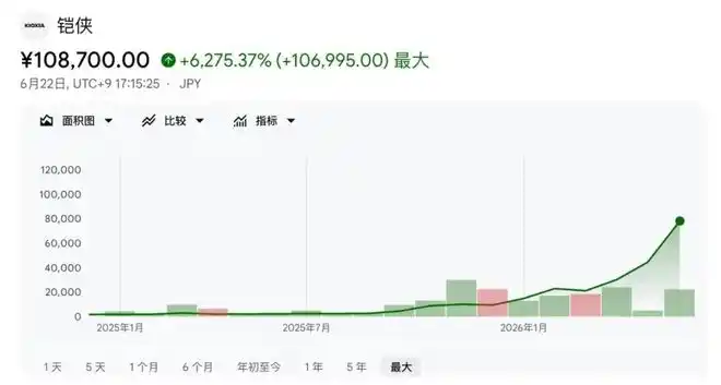
Perjalanan harga saham Kioxia sejak listing

Mitos Super di Pasar Modal

Kioxia berhasil listing di Bursa Efek Tokyo pada akhir tahun 2024, dengan kapitalisasi pasar awal hanya berkisar di 800 miliar yen (sekitar 50 miliar USD). Namun, seiring dengan ledakan penuh permintaan memori AI, Kioxia melakukan kebangkitan epik dalam 18 bulan setelah listing: harga sahamnya melonjak lebih dari 50 kali lipat dalam 18 bulan, hanya dalam tahun 2026 saja naik 8 kali lipat.

Saat ini, kapitalisasi pasar Kioxia telah menembus 51 triliun yen (setara dengan 481 triliun won), beberapa kali melampaui simbol manufaktur Jepang - Toyota Motor, menjadi perusahaan dengan kapitalisasi pasar terbesar di pasar saham Jepang.

Berdasarkan perkiraan kinerja Kioxia untuk kuartal pertama tahun fiskal 2026 (April-Juni), laba operasional kuartal tunggalnya diperkirakan mencapai 1,3 triliun yen (sekitar 81 miliar USD), meningkat hampir 30 kali lipat secara tahunan; panduan laba bersih kuartal tunggal mencapai 869 miliar yen, meningkat 48 kali lipat, kinerja satu kuartal saja telah melampaui perkiraan laba bersih tahunan tahun fiskal 2025.

Karena klien besar berebut menandatangani kontrak pasokan jangka panjang, kapasitas NAND Kioxia tahun 2026 telah habis terjual, situasi permintaan melebihi pasokan diperkirakan akan berlanjut hingga tahun 2027. Pasar memperkirakan, margin laba operasional Kioxia tahun ini akan melebihi 60%, menciptakan tingkat profitabilitas tertinggi dalam industri memori global. Selain itu, dengan harapan pasar bahwa pemegang saham akan menerima pemecahan saham dan dividen, harga saham targetnya diharapkan naik hingga 200.000 yen.

Gelombang kenaikan ini membuat perusahaan induk Bain Capital yang bertahan di periode rendah serta pemegang saham besar tidak langsung SK Hynix meraih imbal hasil investasi di luar dugaan.

Menurut Financial Times, demam AI telah membuat akuisisi Bain tahun 2018 terhadap Toshiba Memory (sekarang Kioxia) menjadi salah satu transaksi ekuitas swasta paling menguntungkan dalam sejarah. Bain Capital telah merealisasikan keuntungan dengan menjual sebagian besar saham, laba melebihi 15 miliar USD, tingkat pengembalian mendekati 20 kali lipat, dana ekuitas swasta andalannya diperkirakan telah memperoleh laba lebih dari 8 miliar USD.

SK Hynix pada tahun 2018 berinvestasi total 395 miliar yen (saat itu sekitar 3,9 triliun won) ke Toshiba Memory melalui konsorsium Korea-AS-Jepang dll. Saat ini, konsorsium tersebut masih memegang 18% saham Kioxia. Dengan kenaikan harga saham Kioxia yang drastis, SK Hynix mendapatkan keuntungan buku yang sangat besar, pasar memperkirakan total laba akhir yang akan diperoleh konsorsium ini jauh melebihi 70 miliar USD.

"Aset panas" yang semula menjadi "mesin penarikan super".

Di masa lalu, dividen kecerdasan buatan terutama terkonsentrasi pada perusahaan GPU dan HBM seperti Nvidia dan SK Hynix. HBM adalah bintang di sisi pelatihan AI, sementara NAND menjadi sumber daya langka dalam inferensi AI, penyimpanan model, danau data, SSD tingkat perusahaan, dan penyimpanan nearline. Pasar memperkirakan, laba bersih Kioxia tahun fiskal 2027 akan mencapai 2,8389 triliun yen, meningkat 5,1 kali lipat dibandingkan tahun sebelumnya.

3D NAND, Fondasi Hidup Kioxia

Kioxia (KIOXIA) menemukan memori flash NAND lebih dari 35 tahun yang lalu. Pada tahun 2007, Kioxia meluncurkan memori flash 3D BiCS FLASH, yang merupakan sistem teknologi memori flash 3D yang berpusat pada penumpukan vertikal, penskalaan lateral, bonding wafer, optimisasi select gate, dan kemasan lanjutan.

Ide dasar 3D NAND adalah: berbeda dengan 2D NAND, tidak hanya mengecilkan sel pada bidang datar, tetapi seperti membangun gedung tinggi, menumpuk sel memori ke arah vertikal. Penjelasan Kioxia sangat gamblang: sebelumnya hanya satu lantai, luas tanah terbatas; 3D NAND setara dengan mengubah satu lantai menjadi apartemen bertingkat, menampung lebih banyak "penghuni" di area yang sama.

Sedangkan inti dari BiCS FLASH adalah teknologi pemrosesan massalnya. Logika prosesnya kurang lebih: pertama, menumpuk lapisan elektroda pelat dan lapisan isolasi secara bergantian; kemudian mengebor banyak lubang sekaligus ke arah vertikal; lalu mengisi film penyimpanan muatan dan elektroda kolom di dalam lubang; titik persilangan antara elektroda pelat dan elektroda kolom membentuk satu sel memori. Dari sini dapat dilihat, BiCS FLASH Kioxia bukanlah "membuat sel memori secara terpisah setiap kali menambah satu lapisan" dalam arti tradisional, melainkan membangun struktur terlebih dahulu, kemudian melalui cara "punch and plug" menembus banyak lapisan sekaligus dan membentuk sel memori. Oleh karena itu, ketika jumlah lapisan bertambah, biaya produksi tidak akan naik secara linear sepenuhnya, sehingga meningkatkan kelayakan ekonomi penumpukan 3D NAND lebih lanjut.

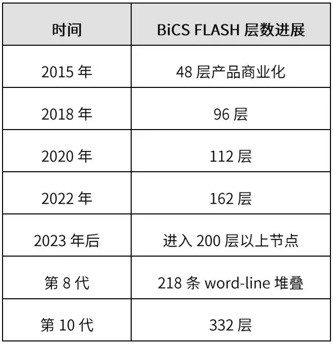
Ritme komersialisasi BiCS FLASH yang diungkapkan resmi oleh Kioxia kurang lebih sebagai berikut, produk BiCS FLASH telah dikomersialkan dengan 48 lapisan pada tahun 2015, kemudian dilanjutkan ke 96 lapisan, 112 lapisan, 162 lapisan; hingga Maret 2023, telah mencapai penumpukan di atas 200 lapisan.

Di antaranya, BiCS FLASH generasi ke-8 adalah titik kritis. Kioxia menyatakan, produk generasi ke-8 menggunakan penumpukan 218 word-line, densitas penyimpanan produk TLC 1Tb mencapai 18,3Gb/mm2, dan mendukung kecepatan transfer data eksternal 3,2Gbps, waktu baca 40μs, dan throughput pemrograman 205MB/s.

BiCS FLASH generasi ke-8 Kioxia tidak hanya melonjak dari 162 lapisan menjadi 218 lapisan, tetapi juga memperkenalkan dua teknologi kunci:

CBA (CMOS Directly Bonded to Array): CBA dapat dipahami sebagai memisahkan pembuatan sirkuit kontrol CMOS periferal dan array memori, kemudian melakukan bonding wafer. Sebelumnya, sirkuit CMOS dan array memori diproduksi pada wafer yang sama. Namun, kondisi proses terbaik yang dibutuhkan keduanya tidak sepenuhnya sama: array memori mungkin membutuhkan proses yang lebih cocok untuk penyimpanan muatan dan struktur penumpukan, sementara sirkuit CMOS lebih fokus pada kontrol logika, performa listrik, dan kecepatan. Meletakkan keduanya pada wafer yang sama akan saling mengkompromikan.

Cara kerja CBA adalah: wafer CMOS dibuat terpisah, wafer array memori dibuat terpisah, keduanya mengoptimalkan proses masing-masing, akhirnya dibonding bersama dengan presisi tinggi. Manfaat yang didapat adalah: meningkatkan bit density, meningkatkan kecepatan I/O NAND, memungkinkan array memori menggunakan proses suhu tinggi yang sebelumnya sulit digunakan karena keterbatasan CMOS, mengurangi interferensi listrik antar sel memori yang berdekatan.

OPS (On Pitch Select Gate): OPS memecahkan masalah pemborosan ruang di dalam array memori. Dalam struktur tradisional, akan ada area "dummy" di antara sel memori yang tidak digunakan untuk menyimpan data. Area ini tidak secara langsung berkontribusi pada kapasitas, tetapi memakan area. Teknologi OPS Kioxia dengan mengatur ulang struktur select gate dan isolasi, mengurangi atau menghilangkan area tidak efektif ini, memungkinkan lebih banyak sel memori efektif dimasukkan ke dalam area yang sama. Penjelasan resmi Kioxia menyatakan, OPS menghilangkan area dummy yang tidak perlu, sehingga lebih banyak sel memori aktual dapat dimasukkan ke dalam ruang yang sama, secara signifikan meningkatkan densitas penyimpanan.
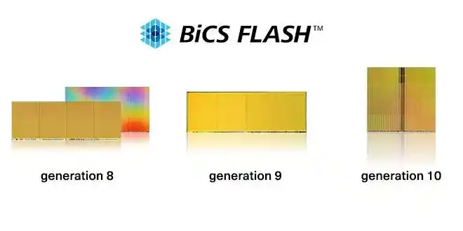
BiCS FLASH generasi ke-9 terutama ditujukan untuk produk TLC 512Gb dan 1Tb, dengan posisi mendukung aplikasi yang memerlukan performa tinggi dan konsumsi daya rendah dalam rentang kapasitas menengah-rendah. Ia terus menggunakan teknologi CBA dan OPS, untuk meningkatkan efisiensi produksi dan menyediakan solusi memori flash yang lebih canggih. Generasi ke-9 tidak mengambil rute peningkatan jumlah lapisan, tetapi lebih menekankan keseimbangan performa, daya, biaya, dan efisiensi produksi.

Sedangkan BiCS FLASH generasi ke-10 jelas lebih condong ke kebutuhan kapasitas besar dan performa tinggi di masa depan. Kioxia menyatakan, produk generasi ke-10 menggunakan teknologi CMOS yang sama dengan generasi ke-9, sekaligus memperluas jumlah lapisan penyimpanan, mencapai 332 lapisan, sekitar 1,5 kali generasi ke-8, untuk meningkatkan bit density dan efisiensi daya.
Selain proses depan, Kioxia juga mengembangkan kemampuan kemasan belakang. Dokumen resmi menyebutkan, Kioxia mengembangkan memori flash 8TB dalam satu paket, dicapai dengan menumpuk 32 die memori flash, masing-masing 2Tb, dalam satu kemasan. Ini mengandalkan proses belakang lanjutan seperti penipisan wafer, desain material, dan bonding kawat. Penumpukan 32-die ini dapat memasang 32 die 2Tb ke dalam kemasan dengan ketinggian di bawah 2mm, membentuk solusi memori flash 8TB.

Dari 3D NAND Menuju 3D DRAM, Taruhan Baru Kioxia

Kioxia juga sedang memecahkan hambatan lini produk tunggal "produsen NAND murni" dengan senjata rahasia. Mengapa Kioxia membuat 3D DRAM? Ini karena, DRAM juga mencapai bottleneck penskalaan planar yang serupa dengan NAND di masa lalu. Dan sebagai pemain lama 3D NAND, Kioxia juga memiliki keunggulan proses yang telah terverifikasi.

DRAM tradisional yang terus mengecil, akan menghadapi beberapa tantangan: kapasitor penyimpanan semakin sulit mengecil, kebocoran transistor akses meningkat, waktu retensi data memendek, frekuensi refresh meningkat, semakin besar kapasitas, semakin tinggi konsumsi daya refresh. imec dalam sebuah tinjauan teknologi juga menyebutkan, struktur 1T1C DRAM tradisional menghadapi tantangan penskalaan, biaya, dan efisiensi daya, terutama kapasitor besar yang membatasi jalur integrasi 3D, dan semakin kecil transistor, jalur kebocoran semakin jelas, menyebabkan konsumsi daya refresh naik.

Pada Desember 2024, Kioxia mengumumkan pengembangan teknologi OCTRAM (Oxide-Semiconductor Channel Transistor DRAM, yaitu "DRAM Transistor Saluran Semikonduktor Oksida"), ini adalah DRAM 4F2 baru, terdiri dari transistor semikonduktor oksida, sekaligus memiliki arus ON tinggi dan arus OFF sangat rendah. Hasil ini dikembangkan bersama oleh Kioxia dan Nanya Technology, dan dipublikasikan pada IEEE IEDM 2024.
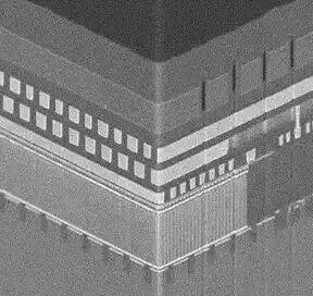
Gambar panorama OCTRAM (Sumber: Kioxia, sama di bawah)

Sel DRAM tradisional umumnya 1T1C, yaitu satu transistor akses ditambah satu kapasitor. Masalahnya adalah: ketika sel terus mengecil, kapasitor semakin sulit dibuat, kebocoran transistor juga akan membuat konsumsi daya refresh menjadi tinggi. OCTRAM Kioxia mencoba mengurangi kebocoran melalui transistor InGaZnO, dan mendorong struktur sel ke densitas yang lebih tinggi.
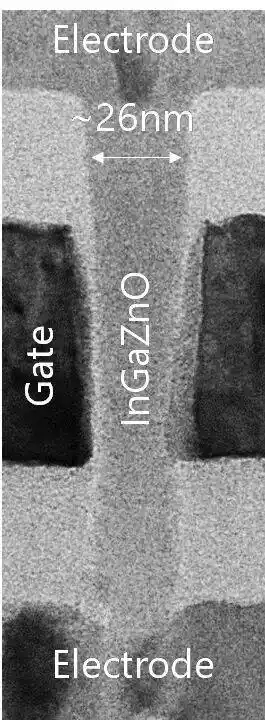
Gambar TEM penampang melintang transistor vertikal InGaZnO

Transistor InGaZnO karena celah pita besar, mobilitas elektron tinggi, secara teoritis dapat mencapai kebocoran sangat rendah dan arus ON tinggi secara bersamaan. Kioxia melalui optimisasi material elektroda kontak dan ketebalan spacer, secara eksperimen mencapai arus ON lebih dari 15μA, sekaligus mencapai kebocoran sangat rendah di bawah 10-18A (seperti gambar di bawah). Konsumsi daya DRAM sebagian besar berasal dari refresh. Semakin rendah kebocoran, semakin panjang waktu retensi data, tekanan refresh semakin kecil. Oleh karena itu, nilai inti OCTRAM adalah menggunakan transistor semikonduktor oksida dengan kebocoran rendah, untuk mengurangi konsumsi daya refresh DRAM.
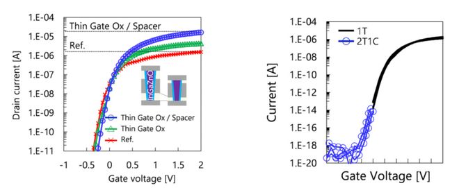
(a) Karakteristik arus ON transistor InGaZnO yang dikembangkan dan (b) Karakteristik arus OFF

Pada September 2025, Kioxia kembali mengungkap penelitian reliabilitas terkait OCTRAM, fokus pada masalah masa pakai TDDB transistor vertikal InGaZnO Gate-All-Around sub-25nm. TDDB adalah Time-Dependent Dielectric Breakdown, yaitu kerusakan dielektrik tergantung waktu. Singkatnya, apakah lapisan isolasi transistor akan secara bertahap terdegradasi dan akhirnya gagal di bawah tekanan medan listrik jangka panjang. Kioxia menyatakan, mereka menemukan degradasi masa pakai berasal dari dua faktor: satu adalah faktor intrinsik akibat penskalaan ukuran, dua adalah faktor ekstrinsik akibat proses manufaktur. Dengan mengoptimalkan proses dan mengurangi degradasi ekstrinsik, Kioxia mencapai perkiraan masa pakai TDDB lebih dari 10 tahun.

Pada Desember 2025, Kioxia mengumumkan kemajuan inti yang lebih mendekati 3D DRAM: mengembangkan transistor saluran semikonduktor oksida yang dapat ditumpuk tinggi, telah mempersiapkan penumpukan transistor horizontal 8 lapis, arus ON melebihi 30μA, arus OFF di bawah 1aA, yaitu 10-18A.

Hingga saat ini, 3D DRAM Kioxia masih dalam tahap penelitian terdepan, bukan produk komersial.

Kioxia bukan raksasa DRAM tradisional, tetapi akumulasi kemampuan proses penumpukan, integrasi material, dan manufaktur array dari 3D NAND, mungkin memberikannya titik masuk dalam eksplorasi 3D DRAM generasi berikutnya. Semiconductor Engineering juga menganalisis, jalur 3D DRAM Kioxia ini meminjam kemampuan penumpukan oksida/nitrida yang matang dari NAND, untuk mencapai penskalaan bit yang lebih rendah biaya, kemudian melalui penggantian saluran IGZO mengurangi masalah degradasi termal.

Tetapi ada satu hal yang harus ditekankan, 3D DRAM Kioxia bukanlah HBM. HBM adalah 3D tingkat kemasan, ia menumpuk die DRAM yang sudah dibuat, menyelesaikan masalah bandwidth tinggi di samping GPU. 3D DRAM Kioxia adalah 3D tingkat perangkat/sel, ia ingin menyelesaikan masalah penskalaan sel DRAM itu sendiri. Jadi Kioxia tidak secara langsung mengejar HBM, tetapi mengeksplorasi jalur perangkat 3D DRAM yang lebih mendasar. Jika jalur ini matang di masa depan, ia mungkin membuka cabang teknologi baru untuk memori kerja kapasitas besar dan konsumsi daya rendah di era AI.

Meskipun 3D DRAM masih jauh dari komersialisasi nyata. Saat ini lebih seperti tiket teknologi menghadapi masa depan, bukan lini produk yang langsung berkontribusi pendapatan. Tetapi bagi Kioxia, makna tiket ini tidak kecil. Jangka pendek Kioxia dapat menikmati pemulihan NAND yang dibawa AI, jangka menengah memajukan BiCS FLASH lapisan tinggi, jangka panjang bertaruh pada 3D DRAM, meluaskan kemampuan penumpukan 3D dari NAND ke DRAM.

Kesimpulan

Dari kerugian besar, kebuntuan merger, hingga melampaui Toyota menjadi nomor satu kapitalisasi pasar Jepang tahun 2026, jalur roller coaster Kioxia, hampir dipenuhi dengan kekejaman dan pesona industri memori semikonduktor. Ia pernah diabaikan pasar modal karena lini produk tunggal dan kehilangan HBM, namun dalam tsunami "aliran data masif" yang dipicu model AI besar, dengan ketekunan pada memori flash NAND, menyambut era keemasan miliknya sendiri.

Kebangkitan Kioxia, mungkin belum bisa membuktikan semikonduktor Jepang telah benar-benar bangkit kembali. Tetapi setidaknya ia membuktikan satu hal: dalam industri semikonduktor, titik rendah tidak selalu menuju ke eliminasi. Selama aset teknologi masih ada, pengaturan ulang siklus, modal, dan permintaan, setiap saat dapat membuat perusahaan yang terlupakan kembali ke pusat meja.

Bagi Kioxia, selanjutnya bagaimana menemukan keseimbangan jangka panjang antara antusiasme modal yang memanas dan siklus industri yang kejam, akan menentukan apakah tunas tunggal yang membawa harapan kebangkitan semikonduktor Jepang ini, hanyalah sekuntum bunga yang mekar sebentar dalam siklus super AI, atau benar-benar membuka kerajaan memori baru miliknya.

*Penyangkalan: Artikel ini ditulis oleh penulis. Isi artikel merupakan pandangan pribadi penulis, Semiconductor Industry Watch hanya menyampaikan pandangan yang berbeda, tidak mewakili dukungan atau persetujuan Semiconductor Industry Watch terhadap pandangan tersebut, jika ada keberatan, silakan hubungi Semiconductor Industry Watch.

Trending Cryptos

Related Questions

QBagaimana cara KIOXIA melakukan lompatan besar dalam 18 bulan setelah IPO?

AKIOXIA mengalami lonjakan harga saham lebih dari 50 kali lipat dalam 18 bulan setelah IPO, terutama didorong oleh ledakan permintaan penyimpanan AI. Model AI besar mengubah logika pasar, membuat NAND flash KIOXIA sangat dibutuhkan untuk inferensi AI, penyimpanan model, dan SSD perusahaan. Ini membalikkan keadaan dari periode kerugian sebelumnya.

QApa teknologi kunci di balik BiCS FLASH generasi ke-8 KIOXIA?

ABiCS FLASH generasi ke-8 KIOXIA menggunakan 218 lapisan word-line dan memperkenalkan dua teknologi kunci: CBA (CMOS directly Bonded to Array) untuk memisahkan dan mengoptimalkan fabrikasi sirkuit CMOS dan array memori sebelum penggabungan wafer, dan OPS (On Pitch Select Gate) untuk menghilangkan area dummy dan meningkatkan kepadatan sel memori yang efektif.

QApa itu OCTRAM dan bagaimana perbedaannya dengan HBM?

AOCTRAM (Oxide-Semiconductor Channel Transistor DRAM) adalah teknologi DRAM 3D yang dikembangkan KIOXIA menggunakan transistor kanal semikonduktor oksida (seperti InGaZnO) untuk mencapai kebocoran arus yang sangat rendah dan mengurangi daya refresh. Berbeda dengan HBM yang merupakan integrasi 3D tingkat paket dari die DRAM yang sudah jadi, OCTRAM adalah pendekatan 3D tingkat perangkat/unit yang bertujuan menskalakan sel DRAM itu sendiri.

QApa dampak keberhasilan KIOXIA terhadap investor awalnya seperti Bain Capital dan SK Hynix?

AKeberhasilan KIOXIA menghasilkan keuntungan luar biasa bagi investor awal. Bain Capital, melalui penjualan sebagian besar saham, memperoleh keuntungan lebih dari $15 miliar dengan pengembalian hampir 20x. SK Hynix, yang berinvestasi melalui konsorsium, memegang 18% saham KIOXIA dan diantisipasi akan mendapatkan keuntungan total lebih dari $70 miliar dari kenaikan harga saham yang dramatis.

QMenurut artikel, apa tantangan utama dan peluang masa depan bagi KIOXIA?

ATantangan utama KIOXIA adalah menemukan keseimbangan berkelanjutan antara antusiasme pasar modal dan siklus industri yang keras. Peluangnya terletak pada melanjutkan kepemimpinan teknologi dalam NAND 3D (seperti BiCS FLASH gen 10 dengan 332 lapisan) dan mengembangkan taruhan jangka panjang pada DRAM 3D (OCTRAM), sehingga memperluas keahlian penumpukan 3D-nya dari NAND ke DRAM untuk era AI.

Related Reads

Trading

Spot

Hot Articles

What is SONIC

Sonic: Pioneering the Future of Gaming in Web3 Introduction to Sonic In the ever-evolving landscape of Web3, the gaming industry stands out as one of the most dynamic and promising sectors. At the forefront of this revolution is Sonic, a project designed to amplify the gaming ecosystem on the Solana blockchain. Leveraging cutting-edge technology, Sonic aims to deliver an unparalleled gaming experience by efficiently processing millions of requests per second, ensuring that players enjoy seamless gameplay while maintaining low transaction costs. This article delves into the intricate details of Sonic, exploring its creators, funding sources, operational mechanics, and the timeline of significant events that have shaped its journey. What is Sonic? Sonic is an innovative layer-2 network that operates atop the Solana blockchain, specifically tailored to enhance the existing Solana gaming ecosystem. It accomplishes this through a customised, VM-agnostic game engine paired with a HyperGrid interpreter, facilitating sovereign game economies that roll up back to the Solana platform. The primary goals of Sonic include: Enhanced Gaming Experiences: Sonic is committed to offering lightning-fast on-chain gameplay, allowing players and developers to engage with games at previously unattainable speeds. Atomic Interoperability: This feature enables transactions to be executed within Sonic without the need to redeploy Solana programmes and accounts. This makes the process more efficient and directly benefits from Solana Layer1 services and liquidity. Seamless Deployment: Sonic allows developers to write for Ethereum Virtual Machine (EVM) based systems and execute them on Solana’s SVM infrastructure. This interoperability is crucial for attracting a broader range of dApps and decentralised applications to the platform. Support for Developers: By offering native composable gaming primitives and extensible data types - dining within the Entity-Component-System (ECS) framework - game creators can craft intricate business logic with ease. Overall, Sonic's unique approach not only caters to players but also provides an accessible and low-cost environment for developers to innovate and thrive. Creator of Sonic The information regarding the creator of Sonic is somewhat ambiguous. However, it is known that Sonic's SVM is owned by the company Mirror World. The absence of detailed information about the individuals behind Sonic reflects a common trend in several Web3 projects, where collective efforts and partnerships often overshadow individual contributions. Investors of Sonic Sonic has garnered considerable attention and support from various investors within the crypto and gaming sectors. Notably, the project raised an impressive $12 million during its Series A funding round. The round was led by BITKRAFT Ventures, with other notable investors including Galaxy, Okx Ventures, Interactive, Big Brain Holdings, and Mirana. This financial backing signifies the confidence that investment foundations have in Sonic’s potential to revolutionise the Web3 gaming landscape, further validating its innovative approaches and technologies. How Does Sonic Work? Sonic utilises the HyperGrid framework, a sophisticated parallel processing mechanism that enhances its scalability and customisability. Here are the core features that set Sonic apart: Lightning Speed at Low Costs: Sonic offers one of the fastest on-chain gaming experiences compared to other Layer-1 solutions, powered by the scalability of Solana’s virtual machine (SVM). Atomic Interoperability: Sonic enables transaction execution without redeployment of Solana programmes and accounts, effectively streamlining the interaction between users and the blockchain. EVM Compatibility: Developers can effortlessly migrate decentralised applications from EVM chains to the Solana environment using Sonic’s HyperGrid interpreter, increasing the accessibility and integration of various dApps. Ecosystem Support for Developers: By exposing native composable gaming primitives, Sonic facilitates a sandbox-like environment where developers can experiment and implement business logic, greatly enhancing the overall development experience. Monetisation Infrastructure: Sonic natively supports growth and monetisation efforts, providing frameworks for traffic generation, payments, and settlements, thereby ensuring that gaming projects are not only viable but also sustainable financially. Timeline of Sonic The evolution of Sonic has been marked by several key milestones. Below is a brief timeline highlighting critical events in the project's history: 2022: The Sonic cryptocurrency was officially launched, marking the beginning of its journey in the Web3 gaming arena. 2024: June: Sonic SVM successfully raised $12 million in a Series A funding round. This investment allowed Sonic to further develop its platform and expand its offerings. August: The launch of the Sonic Odyssey testnet provided users with the first opportunity to engage with the platform, offering interactive activities such as collecting rings—a nod to gaming nostalgia. October: SonicX, an innovative crypto game integrated with Solana, made its debut on TikTok, capturing the attention of over 120,000 users within a short span. This integration illustrated Sonic’s commitment to reaching a broader, global audience and showcased the potential of blockchain gaming. Key Points Sonic SVM is a revolutionary layer-2 network on Solana explicitly designed to enhance the GameFi landscape, demonstrating great potential for future development. HyperGrid Framework empowers Sonic by introducing horizontal scaling capabilities, ensuring that the network can handle the demands of Web3 gaming. Integration with Social Platforms: The successful launch of SonicX on TikTok displays Sonic’s strategy to leverage social media platforms to engage users, exponentially increasing the exposure and reach of its projects. Investment Confidence: The substantial funding from BITKRAFT Ventures, among others, emphasizes the robust backing Sonic has, paving the way for its ambitious future. In conclusion, Sonic encapsulates the essence of Web3 gaming innovation, striking a balance between cutting-edge technology, developer-centric tools, and community engagement. As the project continues to evolve, it is poised to redefine the gaming landscape, making it a notable entity for gamers and developers alike. As Sonic moves forward, it will undoubtedly attract greater interest and participation, solidifying its place within the broader narrative of blockchain gaming.

1.8k Total ViewsPublished 2024.04.04Updated 2024.12.03

What is SONIC

What is $S$

Understanding SPERO: A Comprehensive Overview Introduction to SPERO As the landscape of innovation continues to evolve, the emergence of web3 technologies and cryptocurrency projects plays a pivotal role in shaping the digital future. One project that has garnered attention in this dynamic field is SPERO, denoted as SPERO,$$s$. This article aims to gather and present detailed information about SPERO, to help enthusiasts and investors understand its foundations, objectives, and innovations within the web3 and crypto domains. What is SPERO,$$s$? SPERO,$$s$ is a unique project within the crypto space that seeks to leverage the principles of decentralisation and blockchain technology to create an ecosystem that promotes engagement, utility, and financial inclusion. The project is tailored to facilitate peer-to-peer interactions in new ways, providing users with innovative financial solutions and services. At its core, SPERO,$$s$ aims to empower individuals by providing tools and platforms that enhance user experience in the cryptocurrency space. This includes enabling more flexible transaction methods, fostering community-driven initiatives, and creating pathways for financial opportunities through decentralised applications (dApps). The underlying vision of SPERO,$$s$ revolves around inclusiveness, aiming to bridge gaps within traditional finance while harnessing the benefits of blockchain technology. Who is the Creator of SPERO,$$s$? The identity of the creator of SPERO,$$s$ remains somewhat obscure, as there are limited publicly available resources providing detailed background information on its founder(s). This lack of transparency can stem from the project's commitment to decentralisation—an ethos that many web3 projects share, prioritising collective contributions over individual recognition. By centring discussions around the community and its collective goals, SPERO,$$s$ embodies the essence of empowerment without singling out specific individuals. As such, understanding the ethos and mission of SPERO remains more important than identifying a singular creator. Who are the Investors of SPERO,$$s$? SPERO,$$s$ is supported by a diverse array of investors ranging from venture capitalists to angel investors dedicated to fostering innovation in the crypto sector. The focus of these investors generally aligns with SPERO's mission—prioritising projects that promise societal technological advancement, financial inclusivity, and decentralised governance. These investor foundations are typically interested in projects that not only offer innovative products but also contribute positively to the blockchain community and its ecosystems. The backing from these investors reinforces SPERO,$$s$ as a noteworthy contender in the rapidly evolving domain of crypto projects. How Does SPERO,$$s$ Work? SPERO,$$s$ employs a multi-faceted framework that distinguishes it from conventional cryptocurrency projects. Here are some of the key features that underline its uniqueness and innovation: Decentralised Governance: SPERO,$$s$ integrates decentralised governance models, empowering users to participate actively in decision-making processes regarding the project’s future. This approach fosters a sense of ownership and accountability among community members. Token Utility: SPERO,$$s$ utilises its own cryptocurrency token, designed to serve various functions within the ecosystem. These tokens enable transactions, rewards, and the facilitation of services offered on the platform, enhancing overall engagement and utility. Layered Architecture: The technical architecture of SPERO,$$s$ supports modularity and scalability, allowing for seamless integration of additional features and applications as the project evolves. This adaptability is paramount for sustaining relevance in the ever-changing crypto landscape. Community Engagement: The project emphasises community-driven initiatives, employing mechanisms that incentivise collaboration and feedback. By nurturing a strong community, SPERO,$$s$ can better address user needs and adapt to market trends. Focus on Inclusion: By offering low transaction fees and user-friendly interfaces, SPERO,$$s$ aims to attract a diverse user base, including individuals who may not previously have engaged in the crypto space. This commitment to inclusion aligns with its overarching mission of empowerment through accessibility. Timeline of SPERO,$$s$ Understanding a project's history provides crucial insights into its development trajectory and milestones. Below is a suggested timeline mapping significant events in the evolution of SPERO,$$s$: Conceptualisation and Ideation Phase: The initial ideas forming the basis of SPERO,$$s$ were conceived, aligning closely with the principles of decentralisation and community focus within the blockchain industry. Launch of Project Whitepaper: Following the conceptual phase, a comprehensive whitepaper detailing the vision, goals, and technological infrastructure of SPERO,$$s$ was released to garner community interest and feedback. Community Building and Early Engagements: Active outreach efforts were made to build a community of early adopters and potential investors, facilitating discussions around the project’s goals and garnering support. Token Generation Event: SPERO,$$s$ conducted a token generation event (TGE) to distribute its native tokens to early supporters and establish initial liquidity within the ecosystem. Launch of Initial dApp: The first decentralised application (dApp) associated with SPERO,$$s$ went live, allowing users to engage with the platform's core functionalities. Ongoing Development and Partnerships: Continuous updates and enhancements to the project's offerings, including strategic partnerships with other players in the blockchain space, have shaped SPERO,$$s$ into a competitive and evolving player in the crypto market. Conclusion SPERO,$$s$ stands as a testament to the potential of web3 and cryptocurrency to revolutionise financial systems and empower individuals. With a commitment to decentralised governance, community engagement, and innovatively designed functionalities, it paves the way toward a more inclusive financial landscape. As with any investment in the rapidly evolving crypto space, potential investors and users are encouraged to research thoroughly and engage thoughtfully with the ongoing developments within SPERO,$$s$. The project showcases the innovative spirit of the crypto industry, inviting further exploration into its myriad possibilities. While the journey of SPERO,$$s$ is still unfolding, its foundational principles may indeed influence the future of how we interact with technology, finance, and each other in interconnected digital ecosystems.

99 Total ViewsPublished 2024.12.17Updated 2024.12.17

What is $S$

What is AGENT S

Agent S: The Future of Autonomous Interaction in Web3 Introduction In the ever-evolving landscape of Web3 and cryptocurrency, innovations are constantly redefining how individuals interact with digital platforms. One such pioneering project, Agent S, promises to revolutionise human-computer interaction through its open agentic framework. By paving the way for autonomous interactions, Agent S aims to simplify complex tasks, offering transformative applications in artificial intelligence (AI). This detailed exploration will delve into the project's intricacies, its unique features, and the implications for the cryptocurrency domain. What is Agent S? Agent S stands as a groundbreaking open agentic framework, specifically designed to tackle three fundamental challenges in the automation of computer tasks: Acquiring Domain-Specific Knowledge: The framework intelligently learns from various external knowledge sources and internal experiences. This dual approach empowers it to build a rich repository of domain-specific knowledge, enhancing its performance in task execution. Planning Over Long Task Horizons: Agent S employs experience-augmented hierarchical planning, a strategic approach that facilitates efficient breakdown and execution of intricate tasks. This feature significantly enhances its ability to manage multiple subtasks efficiently and effectively. Handling Dynamic, Non-Uniform Interfaces: The project introduces the Agent-Computer Interface (ACI), an innovative solution that enhances the interaction between agents and users. Utilizing Multimodal Large Language Models (MLLMs), Agent S can navigate and manipulate diverse graphical user interfaces seamlessly. Through these pioneering features, Agent S provides a robust framework that addresses the complexities involved in automating human interaction with machines, setting the stage for myriad applications in AI and beyond. Who is the Creator of Agent S? While the concept of Agent S is fundamentally innovative, specific information about its creator remains elusive. The creator is currently unknown, which highlights either the nascent stage of the project or the strategic choice to keep founding members under wraps. Regardless of anonymity, the focus remains on the framework's capabilities and potential. Who are the Investors of Agent S? As Agent S is relatively new in the cryptographic ecosystem, detailed information regarding its investors and financial backers is not explicitly documented. The lack of publicly available insights into the investment foundations or organisations supporting the project raises questions about its funding structure and development roadmap. Understanding the backing is crucial for gauging the project's sustainability and potential market impact. How Does Agent S Work? At the core of Agent S lies cutting-edge technology that enables it to function effectively in diverse settings. Its operational model is built around several key features: Human-like Computer Interaction: The framework offers advanced AI planning, striving to make interactions with computers more intuitive. By mimicking human behaviour in tasks execution, it promises to elevate user experiences. Narrative Memory: Employed to leverage high-level experiences, Agent S utilises narrative memory to keep track of task histories, thereby enhancing its decision-making processes. Episodic Memory: This feature provides users with step-by-step guidance, allowing the framework to offer contextual support as tasks unfold. Support for OpenACI: With the ability to run locally, Agent S allows users to maintain control over their interactions and workflows, aligning with the decentralised ethos of Web3. Easy Integration with External APIs: Its versatility and compatibility with various AI platforms ensure that Agent S can fit seamlessly into existing technological ecosystems, making it an appealing choice for developers and organisations. These functionalities collectively contribute to Agent S's unique position within the crypto space, as it automates complex, multi-step tasks with minimal human intervention. As the project evolves, its potential applications in Web3 could redefine how digital interactions unfold. Timeline of Agent S The development and milestones of Agent S can be encapsulated in a timeline that highlights its significant events: September 27, 2024: The concept of Agent S was launched in a comprehensive research paper titled “An Open Agentic Framework that Uses Computers Like a Human,” showcasing the groundwork for the project. October 10, 2024: The research paper was made publicly available on arXiv, offering an in-depth exploration of the framework and its performance evaluation based on the OSWorld benchmark. October 12, 2024: A video presentation was released, providing a visual insight into the capabilities and features of Agent S, further engaging potential users and investors. These markers in the timeline not only illustrate the progress of Agent S but also indicate its commitment to transparency and community engagement. Key Points About Agent S As the Agent S framework continues to evolve, several key attributes stand out, underscoring its innovative nature and potential: Innovative Framework: Designed to provide an intuitive use of computers akin to human interaction, Agent S brings a novel approach to task automation. Autonomous Interaction: The ability to interact autonomously with computers through GUI signifies a leap towards more intelligent and efficient computing solutions. Complex Task Automation: With its robust methodology, it can automate complex, multi-step tasks, making processes faster and less error-prone. Continuous Improvement: The learning mechanisms enable Agent S to improve from past experiences, continually enhancing its performance and efficacy. Versatility: Its adaptability across different operating environments like OSWorld and WindowsAgentArena ensures that it can serve a broad range of applications. As Agent S positions itself in the Web3 and crypto landscape, its potential to enhance interaction capabilities and automate processes signifies a significant advancement in AI technologies. Through its innovative framework, Agent S exemplifies the future of digital interactions, promising a more seamless and efficient experience for users across various industries. Conclusion Agent S represents a bold leap forward in the marriage of AI and Web3, with the capacity to redefine how we interact with technology. While still in its early stages, the possibilities for its application are vast and compelling. Through its comprehensive framework addressing critical challenges, Agent S aims to bring autonomous interactions to the forefront of the digital experience. As we move deeper into the realms of cryptocurrency and decentralisation, projects like Agent S will undoubtedly play a crucial role in shaping the future of technology and human-computer collaboration.

767 Total ViewsPublished 2025.01.14Updated 2025.01.14

What is AGENT S

Discussions

Welcome to the HTX Community. Here, you can stay informed about the latest platform developments and gain access to professional market insights. Users' opinions on the price of S (S) are presented below.

活动图片