Author: XinGPT
To understand storage, one must first understand what has happened across the entire semiconductor industry chain.
The Starting Point of the Story: Inference Has Surpassed Training
For the past two years, the semiconductor story has always been "NVIDIA + Training Clusters." However, starting in 2026, due to the sudden explosive demand for AI Agents, most notably the explosive growth of Claude Code, Anthropic's ARR surged from $90 billion to $300 billion in just 4 months.
Inference now accounts for 66% of AI computational load, whereas just two or three years ago, this number was only 33%. That is to say, in three years, the positions of inference and training have completely reversed.
And what does this mean?
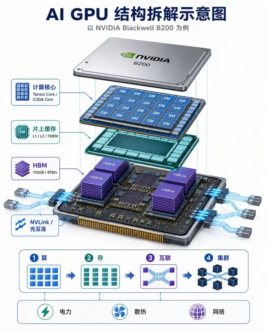
Let's take the NVIDIA Blackwell B200 GPU as an example. Structurally, the B200 is composed of two Blackwell dies connected via the NV-HBI high-bandwidth interface, with die-to-die bandwidth reaching 10TB/s. The entire GPU has approximately 208 billion transistors, 148 SMs, 20,480 CUDA Cores, and 1,024 Tensor Cores, primarily responsible for matrix operations in large models.
Inside the GPU, data flows in layers based on their distance from the computing cores:
The first layer is Registers. They are closest to the computing cores, fastest in speed, and used to hold data currently being computed.
The second layer is L1 / Shared Memory. It is located inside each SM, used to cache short-term, frequently accessed data, reducing access to more distant memory.
The third layer is TMEM, or Tensor Memory. This is an important design introduced by Blackwell for Tensor Cores, intended to bring key data in matrix calculations closer to the computing units, improving Tensor Core utilization.
The fourth layer is L2 Cache. The B200 has approximately 126MB of shared L2 Cache, responsible for caching and reusing data among multiple SMs, especially suitable for repeatedly accessing model weights in inference scenarios.
The fifth layer is HBM3e. The B200 is equipped with 192GB of HBM3e, with a bandwidth of about 8TB/s, serving as the primary storage area for model weights, KV Cache, activation values, and input data. For large model inference, especially during the Decode phase, HBM bandwidth often directly determines token generation speed.
HBM stores large-scale model data, L2 / L1 / TMEM are responsible for delivering high-frequency data to the computing cores step by step, and Tensor Core / CUDA Core perform matrix operations. The calculation results are then written back to the cache or HBM and work collaboratively with other GPUs via NVLink / NV-HBI.
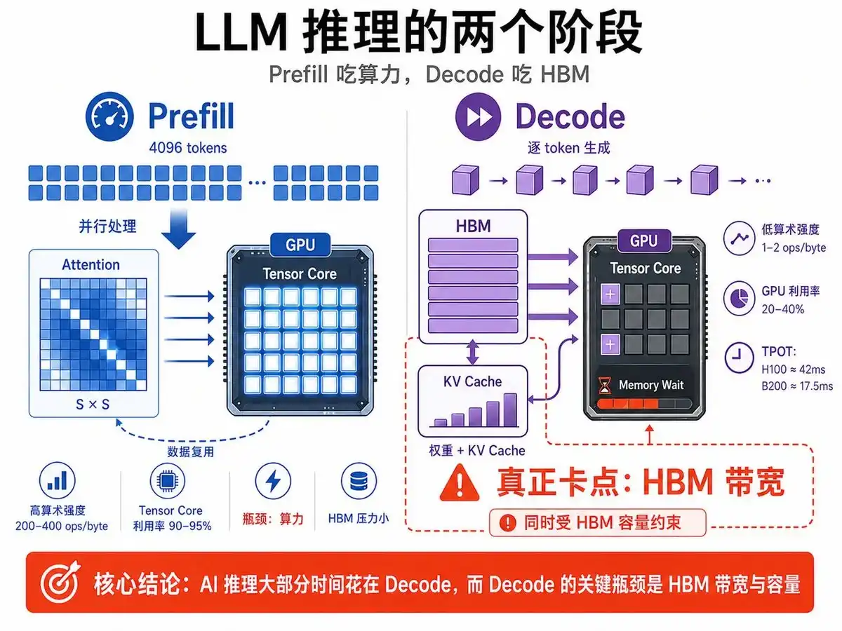
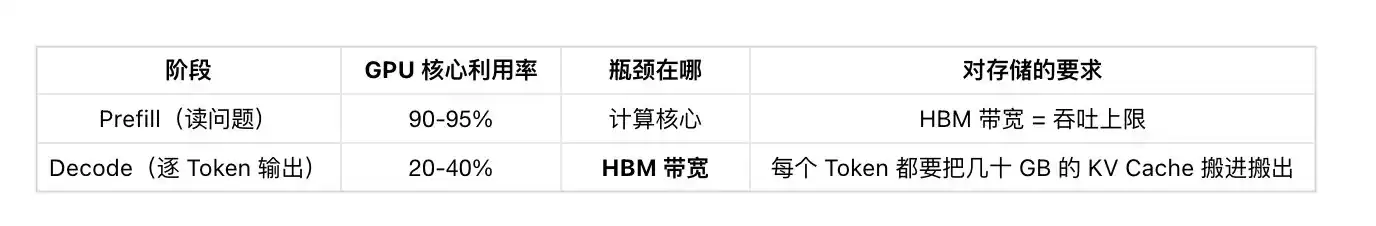
When a GPU performs AI inference, processing a prompt is divided into two phases: Prefill and Decode—which can be roughly understood as "Reading the Question" and "Answering the Question".
Phase One: Prefill (Context Processing, i.e., "Reading the Question")
You input a prompt, say 4096 tokens. The model's first task is to read all 4096 tokens simultaneously, figuring out the relationship between each token and every other token. This is called the Attention Mechanism, which requires calculating an S × S matrix, where S is the sequence length, here S = 4096.
There is a dedicated hardware unit in the GPU for matrix multiplication called the Tensor Core, which can be thought of as a "Matrix Calculator." In this phase, Tensor Core utilization is as high as 90-95%, working at full capacity.
A key concept here is arithmetic intensity, meaning "how many operations can be performed for every 1 byte of data read from memory." In the Prefill phase, this number is 200-400 ops/byte, which is very high, indicating that data read once can be reused many times.
Therefore, the bottleneck in the Prefill phase is computational power (FLOPS, floating-point operations per second), not memory bandwidth; HBM is barely taxed and under little pressure.
Phase Two: Decode (Token Generation, i.e., "Answering the Question")
After the Prefill phase ends, the model enters the Decode phase, which is the token-by-token answer generation stage. Models typically adopt an autoregressive generation mode.
Autoregressive means the model does not generate a complete answer at once, but outputs one token at a time. Each new token generated requires recalculation based on all previously generated tokens. Therefore, the longer the conversation, the heavier the computational burden for subsequent generation becomes.
For the GPU to generate each token, it needs to read two types of critical data from HBM high-bandwidth memory: The first is model weights, i.e., the parameters of the model itself.
The second is KV Cache. KV Cache is the intermediate result cache left by the attention mechanism, where K stands for Key and V for Value. Its purpose is to avoid the model recalculating the attention results for all past tokens every time, thereby accelerating long-text generation. However, the cost is that as the context grows longer, the KV Cache keeps increasing in size, occupying more and more HBM capacity and bandwidth.
For example, a 70B parameter large model, if stored in FP16 precision, the model weights require about 140GB. That is to say, to generate 1 token and complete one forward pass, the GPU needs to read approximately 140GB of weight data from HBM.
The problem is that although the Decode phase reads a lot of data, the actual computation needed is minimal. At this point, arithmetic intensity becomes very low.
In the Decode phase, arithmetic intensity might be only 1-2 ops/byte, meaning only 1-2 operations are performed for every byte read. The result is that Tensor Cores finish computing quickly, but subsequent time is spent waiting for the next batch of data to be delivered from HBM.
This is also why GPU utilization in large model inference is often only 20%-40%. High-end GPUs costing tens of thousands of dollars are often not operating at full computational load but are waiting for memory.
Therefore, the performance bottleneck in the Decode phase has shifted from FLOPS, i.e., theoretical computational power, to HBM bandwidth.
The most intuitive metric is TPOT, Time Per Output Token, meaning how much time is needed to generate each output token.
Taking an H100 running a 70B model as an example, the theoretical physical lower limit in the Decode phase is about 42 milliseconds. This number is primarily determined by the H100's HBM bandwidth. The H100's HBM bandwidth is about 3.35TB/s; if generating one token requires reading about 140GB of data, then the theoretical lower time limit is 140GB ÷ 3.35TB/s ≈ 42ms
Switching to Blackwell B200, with HBM bandwidth increased to about 8TB/s, reading the same 140GB data, the theoretical lower limit becomes: 140GB ÷ 8TB/s ≈ 17.5ms
That is to say, Decode speed increases by about 2.4 times, primarily due to HBM bandwidth improvement.
So, are there ways to alleviate this memory bottleneck?
The most important method is to increase batch size, i.e., have the GPU handle more user requests simultaneously. Because model weights can be shared among multiple requests, the GPU reads the weights once and can serve multiple users at the same time. This way, the memory read cost per user, per token is reduced.
This is also why modern AI inference serving systems all pursue high concurrency and large batch sizes. The larger the batch, the more likely the GPU's computing units are to be fully utilized, and the lower the unit token cost.
But batch size cannot be increased indefinitely because more concurrent requests lead to larger KV Cache. KV Cache needs to reside in HBM for a long time, so HBM capacity also becomes very critical. Bandwidth determines data read speed; capacity determines how many requests can be served simultaneously.
Therefore, the core bottleneck of AI inference can be summarized as: the Prefill phase is more computationally demanding because it processes a large number of input tokens in parallel. The Decode phase is more HBM-dependent because it repeatedly reads model weights and a growing KV Cache.
In practical inference services, most of the time is spent in the Decode phase. Therefore, the core bottleneck determining inference efficiency is the bandwidth and capacity of HBM.
Here is a summary of AI inference economics:
AI inference can be simplified to a core equation: Token Price ∝ (GPU Cost + Power Cost) / (Tokens Generated Per Second)
And Tokens Generated Per Second (Throughput) is directly limited by two physical constraints:
-
HBM Capacity: Determines how large a model a single card can hold, how long a context it can support, and the potential batch size.
-
HBM Bandwidth: Determines the speed of reading model weights and KV Cache from HBM for each token generated.
During the Decode phase (token-by-token output generation), GPU computational utilization is typically extremely low (<10%), because most of the time is spent reading data from HBM. This is a classic Memory-Bound scenario. At this point, HBM bandwidth directly determines token generation speed—doubling bandwidth nearly doubles throughput and nearly halves unit token cost.
When the model parameter count exceeds the HBM capacity of a single card, the system must employ Model Parallelism, distributing weights across multiple cards. Generating each token requires cross-card communication, introducing huge network latency and additional computational overhead. A core reason why OpenAI's early GPT-4 service had slow response times and high costs was that the model was too large, forcing distribution across many GPUs, and communication overhead consumed efficiency.
Therefore, every leap in HBM capacity and bandwidth directly corresponds to an exponential decline in token inference cost:
-
H100 → H200: Capacity +76%, Bandwidth +43% → Supports larger batches and longer contexts
-
B200 → Vera Rubin: Capacity unchanged (288GB), Bandwidth 2.75 times → Significant throughput improvement in Decode phase
-
Rubin Ultra: Capacity 4 times (1TB+)→ Can fit trillion-parameter MoE models within a single card/chassis, eliminating sharding overhead
NVIDIA claims Rubin can achieve a 10x reduction in per-Token Total Cost of Ownership (TCO) compared to Blackwell, essentially derived from the triple effect of HBM4 bandwidth leap (reducing Memory-Bound time) + FP4 precision (reducing data transfer volume) + larger capacity (reducing cross-machine communication).
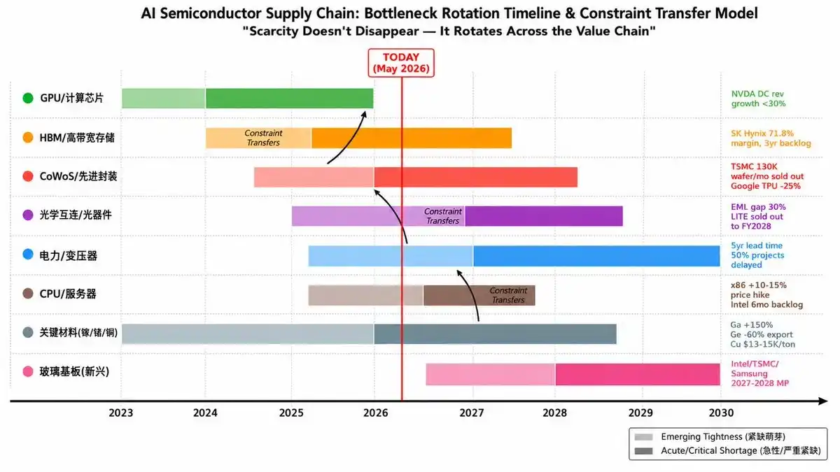
Based on the above semiconductor shortage logic, we evaluate the seven segments of the AI industry chain, resulting in an industrial map of semiconductor sector tightness. We will release detailed research on other sectors subsequently.
Storage Sector Panorama: Classification, Technology Generations, Player List
From DRAM, NAND, NOR to HBM, HBF
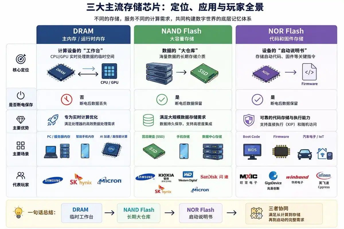
Now, let's return to the storage industry. Storage chips can broadly be divided into two categories: one is "runtime memory," responsible for allowing CPUs, GPUs to quickly read and process data; the other is "long-term storage," responsible for preserving data after power-off.
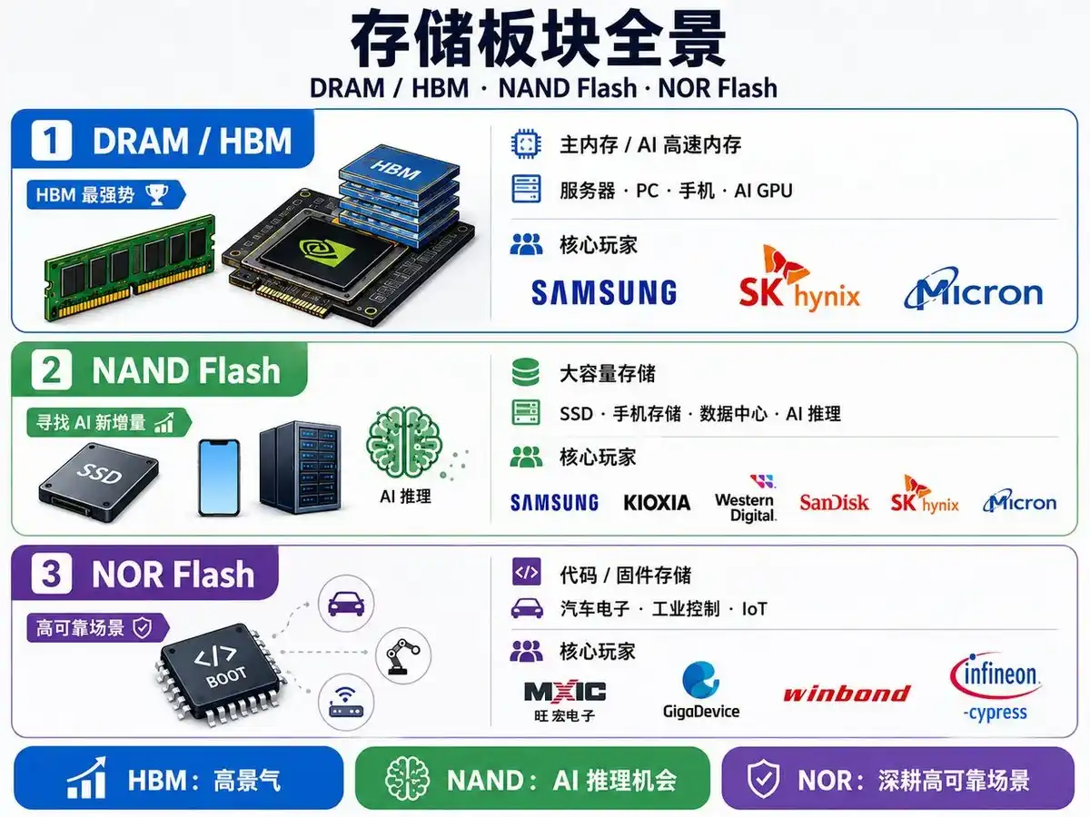
From a product classification perspective, the three core traditional categories are DRAM, NAND Flash, and NOR Flash. Entering the AI era, HBM has become the most important high-end branch within DRAM, while HBF represents a new attempt by NAND Flash to extend into high-bandwidth, high-capacity AI inference scenarios.
Traditional Three Storage Categories: DRAM, NAND, NOR
DRAM is the most typical volatile memory, meaning data disappears after power-off. It primarily serves the role of "runtime data temporary storage" and is the main memory most relied upon by CPUs, GPUs, and other computing chips during operation.
DRAM's advantages are high speed and low latency, suitable for real-time computation; its disadvantages are higher cost and inability to retain data without power. Its technology generations primarily evolve around bandwidth, power consumption, and capacity. Current mainstream products include DDR4, DDR5, as well as GDDR and HBM for graphics and AI acceleration scenarios. DDR5 is gradually replacing DDR4, becoming the mainstream memory standard for servers and high-end PCs.
NAND Flash is the most widely used non-volatile memory, meaning data can be preserved after power-off. It is primarily used in SSDs, smartphone storage, USB drives, memory cards, and data center hard drives. Compared to DRAM, NAND is much slower but offers larger capacity and lower unit cost, making it more suitable as a "large-capacity data warehouse."
NAND technology evolution mainly follows two paths: one is moving from SLC, MLC, TLC to QLC, continuously increasing how many bits each memory cell can store; the other is moving from 2D NAND to 3D NAND, increasing capacity through vertical stacking. Currently, 200-layer+ and 300-layer+ 3D NAND have become the industry's competitive focus. The core contradiction for NAND is the balance between capacity, cost, performance, and endurance. TLC and QLC have lower cost and larger capacity, but weaker write endurance and performance compared to SLC and MLC.
NOR Flash is also non-volatile memory, but its positioning is completely different from NAND. NOR's characteristics are fast read speed, support for random access, and the ability to execute code directly, i.e., XIP (Execute In Place). Therefore, NOR is mainly used to store boot code, firmware, and critical system parameters, such as Boot Code and Firmware in mobile phones, automotive electronics, IoT devices, PC motherboards, and embedded systems.
NOR capacity is typically not large, write and erase speeds are not fast, and cost is higher than NAND, so it's not suitable for large-capacity storage. However, in scenarios like device boot-up, security authentication, automotive electronics, and industrial control, NOR's reliability and fast read capability are crucial. With the increase in automotive electronics and IoT devices, high-density NOR still has structural growth potential.
In short, DRAM is responsible for "runtime computation," NAND is responsible for "large-capacity storage," and NOR is responsible for "boot-up and firmware."
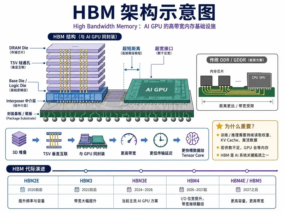
The Most Important Storage Branch in the AI Era: HBM
If traditional DRAM is the main memory for servers and PCs, then HBM is the high-end dedicated memory for AI GPUs. HBM stands for High Bandwidth Memory. It essentially still belongs to DRAM, but its structure and packaging are very different from traditional DDR and GDDR.
Traditional memory typically connects to the processor via PCB traces, and bandwidth improvements are limited by power consumption, distance, and signal integrity. HBM, on the other hand, adopts a 3D stacking structure, vertically stacking multiple layers of DRAM dies and connecting them vertically via TSVs (Through-Silicon Vias). Subsequently, the HBM stack is placed in the same package as the GPU via an Interposer, enabling very short-distance, ultra-wide interface data transmission.
This brings two direct results: First, HBM has extremely high bandwidth; Second, HBM is very close to the GPU, allowing data to be delivered to the computing cores faster. This is crucial for large model training and inference. Because although AI GPU Tensor Cores compute very fast, if HBM cannot timely provide model weights, KV Cache, and activation data, the GPU will experience "memory wait."
Therefore, HBM has become one of the core bottlenecks in AI computing systems. Especially during the Decode phase of large model inference, performance is often no longer determined by the GPU's theoretical FLOPS, but by HBM's bandwidth and capacity. Bandwidth determines the speed at which data is fed to the GPU; capacity determines how many model weights and KV Cache a single card can hold, and how large a batch it can serve simultaneously.
From a technology generation perspective, HBM iteration is rapid. HBM2E was mainly used in early AI acceleration and HPC; HBM3 significantly improved bandwidth; HBM3E is the mainstream configuration for current AI GPUs; HBM4 will further increase I/O width, single-stack bandwidth, and capacity, and introduce more complex base die designs. Future HBM4E, HBM5 will continue evolving towards higher bandwidth and larger capacity.
NAND's New Direction: HBF
HBF (High Bandwidth Flash) is a new type of storage born for AI inference. It can be understood as a "middle-tier high-speed storage" between HBM and ordinary SSDs. AI models are getting larger, with weight files often hundreds of GB, even TB level. HBM is fast enough but capacity limited and expensive; SSDs have sufficient capacity, but speed and latency cannot keep up with high-performance inference demands. The emergence of HBF aims to solve this contradiction.
It borrows HBM's 3D stacking and high-speed interconnect technology, vertically stacking multiple layers of NAND Flash dies and connecting them via high-speed channels, thus possessing much higher bandwidth than ordinary SSDs while maintaining large capacity characteristics. It is not meant to replace HBM, but to serve as a "near-line high-speed storage layer," specifically storing large model weights, so the GPU doesn't frequently wait for data during inference.
By 2026, HBF has entered the engineering sample phase. Manufacturers plan to begin delivering samples in the second half of the year and see the first commercial reference designs in 2027. Mass production is not expected until after 2028. Its significance lies in that AI inference servers can achieve bandwidth and capacity close to HBM at a lower cost than an all-HBM solution, enabling faster large model loading and higher throughput.
Player List: Who Holds Key Positions in the Storage Industry Chain
From a global perspective, the storage industry is highly concentrated, but competitive landscapes differ significantly across product lines, with each player having its core strengths and strategic focus.
DRAM and HBM Field: Samsung, SK Hynix, and Micron are the absolute core players. DRAM remains the main memory for servers, PCs, and mobile devices, while HBM is the critical high-speed memory for AI GPUs. Samsung excels in overall process and packaging integration, especially with advantages in 3D stacking and TSV reliability; SK Hynix, leveraging deep ties with NVIDIA and first-mover advantages in mass production, holds over half of the HBM market share; Micron is rapidly catching up on HBM3E and HBM4 engineering samples, showing notable progress especially in high-capacity stacking and reliability optimization.
For HBM, competition is not only about DRAM manufacturing processes but also TSV stacking, packaging yield, testing processes, customer qualification, and long-term supply capability. Securing large AI chip orders from NVIDIA, AMD, Google, etc., means holding pricing power and guaranteed capacity in the current AI storage supercycle.
NAND Flash Field: Core players include Samsung, Kioxia/Western Digital, SanDisk, SK Hynix, and Micron. In the past, the NAND market was primarily driven by consumer electronics, SSD, and data center demand. With the growth of AI inference demand, the development of high-bandwidth NAND or HBF technology provides new growth opportunities for manufacturers. Samsung still leads in high-density 3D NAND and enterprise SSDs; Kioxia/Western Digital have prominent advantages in storage scale and reliability; SanDisk focuses on HBF and high-bandwidth flash prototypes, rapidly targeting the AI inference market. SK Hynix and Micron are also actively following up on high-bandwidth NAND solutions, competing for AI data center market share.
NOR Flash Field: Major players include Macronix, GigaDevice, Winbond, and Infineon/Cypress. The NOR market size is smaller than DRAM or NAND, but applications are diverse and require high reliability. It's mainly used in automotive electronics, industrial control, IoT, and embedded systems, responsible for storing boot code, firmware, and critical parameters. Chinese manufacturers show relatively strong competitiveness in the NOR field. GigaDevice is continuously breaking through in high-density NOR and automotive-grade applications, steadily growing its market share.
In summary, the storage sector can be divided into three layers according to the AI semiconductor chain:
-
High-End AI Memory Players: Core HBM suppliers like SK Hynix, Samsung, Micron, targeting GPU high-bandwidth memory and large model training demand.
-
Large-Capacity Storage Players: NAND and SSD manufacturers like Samsung, Kioxia/Western Digital, SanDisk, SK Hynix, Micron. The future adoption of HBF will open new growth points in the AI inference market for these players.
-
Embedded and Control-Class Storage Players: NOR Flash suppliers like Macronix, GigaDevice, Winbond, Infineon/Cypress, focusing on scenarios with high reliability requirements like industrial, automotive, and IoT.
This landscape shows the layered trend of the storage industry chain driven by AI: HBM represents high-end computing power support, NAND/HBF represents the combination of large capacity and high bandwidth, and NOR ensures stability for embedded and industrial control. With the advancement of new technologies like HBF, the landscape of NAND and AI inference storage markets may undergo new changes.
We will delve into detailed financial analysis and business research for each company later in subsequent articles.
In-depth Supply-Demand Analysis: The Most Severe Structural Shortage in 15 Years
The current global memory chip market is experiencing a historic boom driven by multiple overlapping demand engines, with AI's explosion at its core. The three forces of AI training, AI inference, and the large-scale global data center expansion intertwine and reinforce each other, collectively forming a "bottomless pit" demand for memory chips. The transmission logic of these three engines differs, but their direction is completely aligned.
Demand Side
Engine One: AI Training—Parameter Arms Race Drives HBM Capacity Expansion
Large language model parameter scales are accelerating from hundreds of billions towards trillions. Each iteration is not linear—GPT-4 has about 1.8 trillion parameters (MoE architecture); the target for next-gen models is 10 trillion+. Training such models requires parallel processing on thousands, even tens of thousands of GPUs for months.
But the real bottleneck in training is the bandwidth between the GPU and HBM. During training, each GPU needs to repeatedly read and write gradients, optimizer states, activation values in HBM. Insufficient HBM capacity → cannot hold the complete model state → must communicate across GPUs → communication overhead consumes computational gains.
Thus, for each generation of NVIDIA's GPU, HBM capacity jumps:
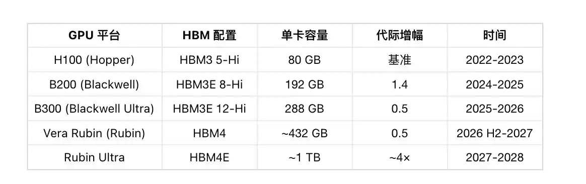
From H100 to Rubin Ultra, single-card HBM capacity surges from 80 GB to ~1 TB, increasing 12.5 times in four years.
And it's not just NVIDIA. Google TPU v8AX, Amazon Trainium3 are also upgrading from HBM3E 8-Hi to 12-Hi. AMD MI350→MI400, HBM capacity jumps from 288 GB to 432 GB. The entire AI accelerator industry is racing in the same direction.
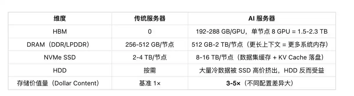
The training phase demands storage across the entire stack:
-
HBM: The GPU's "workbench," where all intermediate states of the training process reside. Without enough HBM → cannot train large models.
-
NVMe SSD: Training datasets can be tens of TB (e.g., Llama 3 used 15T tokens). They must be fed to HBM at high speed. Bottlenecks in data loading directly lengthen training time—if SSD bandwidth cannot keep up with GPU consumption, tens of thousands of GPUs idle waiting for data.
-
HDD: Cold data storage. Post-training model weights, historical checkpoints, raw corpora need long-term preservation.
Engine Two: AI Inference—Scale Effect Makes Storage Demand "Long-Tailed"
The single-shot computational complexity of inference is indeed much lower than training, but its demand characteristics are completely different: Training is a bursty, concentrated consumption; Inference is a continuously expanding, long-tail devouring force.
Several key numbers need to correct traditional perceptions:
Inference is no longer the "small share." In 2026, inference accounts for 66% of total AI computing load; two years ago this number was only 33%. The positions of inference and training have completely reversed. With the explosion of Agentic AI (AI capable of autonomously calling tools, multi-step reasoning, multi-agent collaboration), inference's share will only continue to rise.
Single inference memory demand is severely underestimated. A cutting-edge LLM's model weights occupy 100-200 GB (FP16 precision), and KV Cache consumes an equal or even greater amount of memory. There's a simple, brutal rule for KV Cache: every time the context token count doubles, the memory occupied by KV Cache also doubles. Agentic workloads typically have long contexts (multi-turn conversations, codebase context, document retrieval), making KV Cache pressure far exceed that of simple chatbots.
GPU's role division during inference:
Agentic AI spends most of its time in Decode. This is why HBM bandwidth determines inference speed, and HBM capacity determines how many users can be served simultaneously.
Scale effect is the real story. A training cluster might need thousands of GPUs, but inference deployment might require hundreds of thousands, even millions. Anthropic's ARR grew from $90 billion to $300 billion in just 4 months.
Anthropic itself stated: with more GPUs, ARR could be even higher. They are constrained by HBM supply on GPUs.
Inference's full-stack storage demand:
-
HBM: Core bottleneck for GPU inference (bandwidth + capacity). Long context + KV Cache in Agentic inference continually worsens this bottleneck.
-
Enterprise SSD: Model weight persistence, offloading KV Cache to SSD (long context strategy), user data storage. Enterprise SSD prices increased 140% month-over-month.
-
HBF (High Bandwidth Flash): Next-gen product from the SanDisk and Kioxia collaboration, single stack 512 GB, module 4 TB, designed specifically for inference weight storage. Mass production starts early 2027. If successful, the memory hierarchy for inference will be rewritten—HBM for speed, HBF for capacity.
Engine Three: Data Center Expansion—The "Amplifier" of Storage Value
Hyperscalers' CapEx surge isn't just for AI. Traditional cloud computing, big data, and streaming are also growing. But AI has changed the storage architecture of data centers.
Several specific data points:
-
In 2026, data centers consume ~70% of global DRAM capacity (SemiAnalysis), with server DRAM ~40%, HBM ~10%+ and rising rapidly
-
Seagate's FY2026 Q3 data center shipments accounted for 88%; nearline HDD capacity for 2026-2027 is completely sold out, with orders for 2028 already being discussed
-
Kioxia's 2026 NAND capacity has been 100% booked by customers
-
NVIDIA Vera Rubin NVL72 system memory demand jumps significantly from Blackwell NVL72 levels (SOCAMM LPDDR5-based memory becomes a new growth area)
HDD's unexpected resurgence is a particularly interesting side effect: enterprise SSDs are too expensive (month-over-month +140%), pushing a lot of cold data from SSDs back to HDDs. In the AI inference era, the economics of storage-compute separation give HDDs new survival logic—nearline HDD demand explodes; Seagate's net profit increased 248% year-over-year.
Cross-Validation of the Three Engines
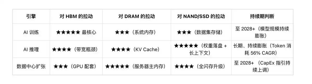
In summary: Training defines the upper limit of HBM capacity, Inference defines the breadth of HBM demand, and Data center expansion provides the base for total demand volume. None of these three forces are slowing down, while the supply side (detailed in the next section) is an "iron cage." This is the underlying narrative of this storage cycle.
Supply Side: HBM Capacity Squeeze and 2-3 Year Capacity Build Cycle
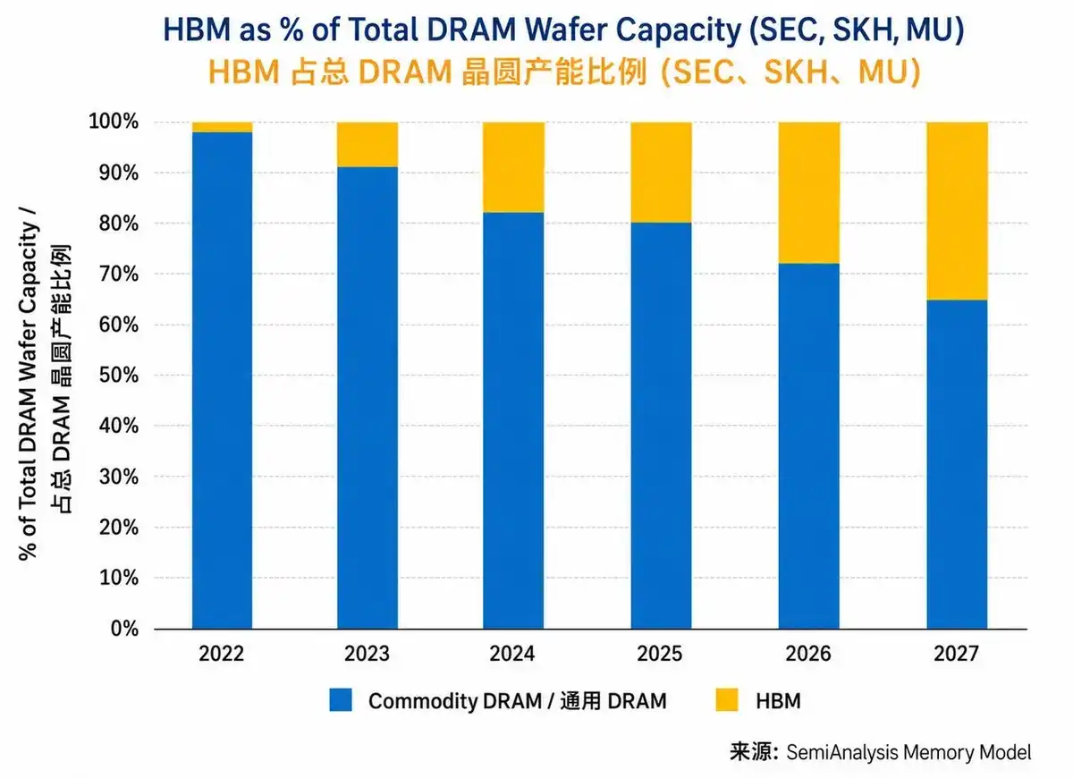
Facing the explosive growth on the demand side, the supply side of memory chips is under unprecedented structural constraints, unable to respond quickly to market changes. This is the fundamental cause of the current severe global memory chip shortage and soaring prices. The core supply-side problems can be summarized in two points: first, the massive squeezing effect of HBM production on traditional DRAM and NAND capacity; second, the inherent 2-3 year long capacity build cycle for memory chips, resulting in extremely low supply elasticity.
According to SemiAnalysis estimates, the proportion of HBM wafer capacity to total DRAM wafer capacity for Samsung, SK Hynix, and Micron was less than 5% in 2022, but by the end of 2025, it had risen to about 20%. By the end of 2027, this proportion might reach about 35%.
First, HBM, as the current "golden goose" of the storage market, has an exceptionally complex and "resource-hungry" production process. As mentioned, HBM uses 3D stacking and TSV (Through-Silicon Via) technology to vertically package multiple DRAM dies together. This complex packaging process not only has high technical barriers and slow yield ramp-up but also consumes 3 to 4 times more wafer area than traditional DRAM products of equivalent value. This means producing a $100 HBM chip consumes the wafer area that could have produced 3-4 standard DRAM chips.
This structural shift in capacity causes severe knock-on effects. Statistics show that to secure HBM output, Samsung shifted about 30% of its consumer-grade DRAM capacity to HBM; SK Hynix's shift ratio is even higher at 40%; and Micron shifted about 25%. These numbers are staggering; they directly lead to a significant reduction in available global standard DRAM capacity.
Simultaneously, because HBM packaging requires advanced packaging lines (like CoWoS), this capacity is also heavily occupied, further limiting other advanced packaging businesses. This "suction effect" triggered by HBM causes markets for DDR4, DDR5, and NAND Flash, which were relatively balanced in supply and demand, to fall into severe shortage within a short period. For example, as DDR4 capacity was drastically reduced, its price experienced a shocking increase in the second half of 2025, rising up to 1800%, fully illustrating the severity of the capacity squeeze.
Thus, we can see this cycle's uniqueness lies in: the product shift driving demand growth—HBM—itself has higher manufacturing intensity, effectively introducing a reverse scaling effect. In past computing platform inflection points, like PCs, mobile phones, cloud computing, they mainly expanded demand without significantly constraining supply. But this time, the shift to HBM driven by AI increases demand on one hand, and on the other, due to HBM's manufacturing difficulty exceeding traditional DRAM, it effectively tightens supply.
Second, the semiconductor capacity build cycle is another major hard constraint on the supply side.
From deciding to invest in building a new wafer fab to finally producing qualified chips typically takes 2 to 3 years. This process includes plant construction, cleanroom setup, procurement, installation, and debugging of multi-million-dollar equipment (like EUV lithography machines), followed by lengthy process development and yield ramp-up.
In the current market environment, even if the three major manufacturers decided tomorrow to aggressively invest in expanding DRAM capacity, these new capacities would only begin to actually enter the market by the end of 2027 or early 2028. More importantly, facing the structural opportunity brought by AI, manufacturers' capital expenditure strategies have become more cautious and focused. They prefer to invest precious capex into higher-margin, more certain growth prospects like HBM and advanced DRAM technology, rather than massively expanding relatively mature, thinner-margin traditional NAND Flash capacity.
For example, SK Hynix plans to build a new advanced packaging plant in Indiana, USA, focusing on AI memory (including HBM); Micron plans to invest tens of billions in new fabs in Idaho and New York, USA—these investments are aimed at future HBM and advanced DRAM capacity, not solving current traditional storage shortages. Therefore, at least until the end of 2027, the market will hardly see any new supply that could significantly alleviate the current supply-demand tension. This supply rigidity, contrasted with demand elasticity, jointly pushes the storage industry into a "long-haul" supercycle.
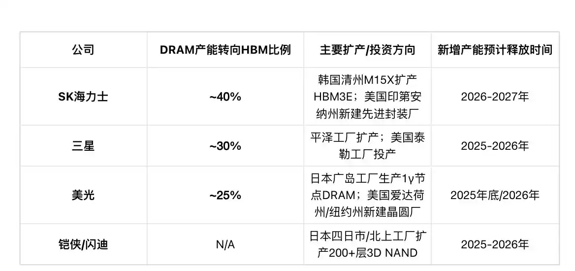
Table 3: Major Manufacturers' Capacity Shift and Expansion Plans
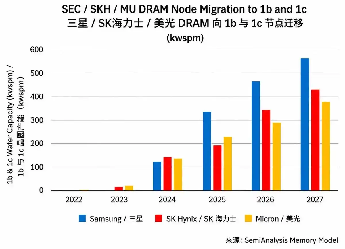
According to estimates, from the end of Q4 2025 to Q4 2027, the combined 1b and 1c capacity of the three major manufacturers will increase by about 80%; by the end of 2026, nearly 30% of Samsung and SK Hynix's DRAM wafer production will shift to the 1c node, and Micron will also shift about 30% of its DRAM production to its corresponding 1γ node.
In 2026, actual new wafer output is limited and concentrated mostly on HBM; NAND sees almost no actual wafer increment.
According to SemiAnalysis data, it's expected that in 2026, almost all new wafer capacity will be concentrated in three fabs: Samsung's P4 (mainly Phase 1 and 3, Phase 4 has limited contribution by end-26), SK Hynix's M15X, and Micron's A3.
Quantifying the Supply-Demand Gap: Goldman Sachs Predicts a 4.9% DRAM Supply Shortage in 2026
The current imbalance in the storage market has reached an extremely severe level. Quantitative analyses by multiple top investment banks provide solid evidence for the strength of this "supercycle." Goldman Sachs released an in-depth research report in mid-2025, clearly stating that the current memory chip market is experiencing the most severe supply-demand imbalance in the past 15 years. Through detailed modeling of global DRAM and NAND Flash supply and demand, the report predicts staggering shortage figures. For the DRAM market, Goldman Sachs predicts supply shortages of 4.9% and 2.5% in 2026 and 2027, respectively. This means total global DRAM demand will exceed total supply by nearly 5%. In a market measured in millions of wafers, such a large-scale shortage is extremely rare, sufficient to trigger sustained, substantial price increases. The situation for NAND Flash is similarly concerning, with the report predicting it will also be in shortage, albeit slightly less severe than DRAM, but given its massive market size, its impact on the entire industry is equally profound.
This quantitative analysis deeply reveals the structural reasons behind the imbalance. Goldman Sachs' model fully considers the squeezing effect of HBM capacity expansion on traditional DRAM capacity and the lag of manufacturers' capital expenditure shifts. The report believes that although manufacturers are aware of the tightness and beginning to increase investment, due to the 2-3 year capacity build cycle, these investments cannot translate into effective supply in the short term. Therefore, the supply-demand gap will persist, possibly even widen, over the next one to two years.
According to calculations from SemiAnalysis's Memory Industry Model, the DRAM market supply-demand imbalance is worsening. In 2026, overall DRAM supply is expected to be about 7% lower than demand.
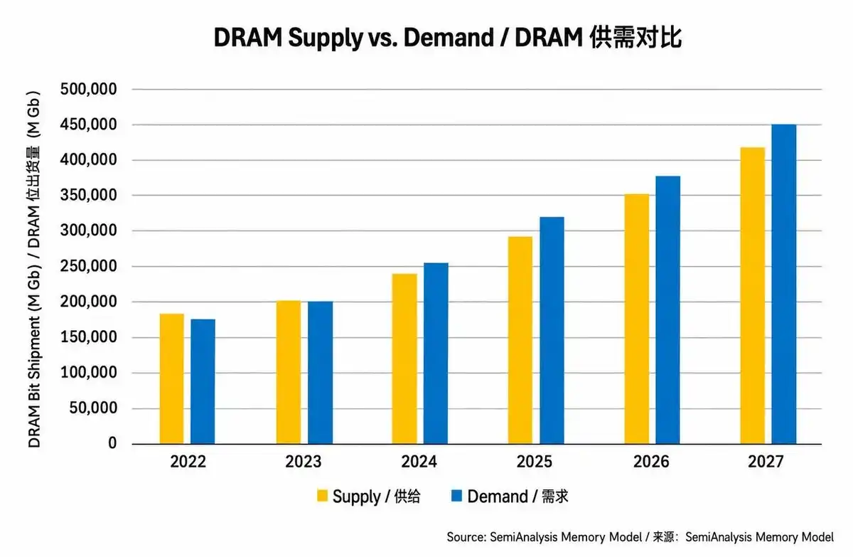
Within this overall shortage, the HBM supply shortage is expected to widen from about 5% this year to about 6% in 2026, and further to about 9% in 2027.
These quantitative figures are not just descriptions of the current market condition but also strong predictions for future price trends and manufacturer profitability. In a severely undersupplied market, pricing power lies entirely with the manufacturers. Customers, especially cloud service providers and AI companies needing stable supply, are willing to accept higher prices and sign long-term supply agreements to ensure sufficient chip supply.
Inventory Status: Inventory Days Drop to Historically Extreme Lows
Inventory level is one of the most sensitive and direct leading indicators for judging the position in the memory chip industry cycle. In a normal industry cycle, downstream customers (like PC makers, smartphone manufacturers, server brands) typically maintain inventory of about 12 to 16 weeks (84-120 days) to cope with demand fluctuations and supply chain uncertainty. However, in the current supercycle, inventory is not a simple buffer but a "barometer" reflecting a state of extreme market hunger. Current inventory levels across the entire storage industry chain have fallen to historically extreme lows.
We analyze inventory across four layers:
Layer 1: DRAM/HBM Manufacturers (Samsung / SK Hynix / Micron / Nanya)
Note: Bloomberg's DOI calculation includes total inventory (including WIP, raw materials, finished goods), while SK Hynix self-disclosed at the Goldman Sachs virtual investor conference in February 2026 that about 4 weeks (28 days) only refers to finished goods inventory for DRAM and NAND. Bloomberg/MacroMicro's latest update (after DART 5/15 cutoff) shows SK Hynix's total inventory DOI is 124.98 days (Q4 2025 was 143 days), Q1 2026 declined 18 days QoQ—finished goods inventory extremely low, many wafers stuck on HBM TSV drilling/stacking production lines. SK Hynix stated in the same conference: "No customer can fully meet their memory demand this year." Micron confirmed in Q1 FY2026 (Dec 2025) and Q2 FY2026 (Mar 2026) earnings calls for two consecutive quarters that DRAM inventory days "remain tight and below 120 days", with Q2 further using the phrase "especially tight".
HBM's TSV drilling, wafer thinning, 12-layer stacking, and testing processes are extremely lengthy; many wafers are stuck on production lines, while finished goods are shipped out immediately upon completion. This is a very dangerous signal, indicating the company's finished goods inventory is shipped out to customers almost simultaneously with completion, leaving almost no surplus stock. This "hand-in-hand" supply state shows market demand is far stronger than official order data indicates, as customers are also consuming their own safety stock.
Layer 2: FLASH / HDD Manufacturers (SanDisk / Western Digital / Seagate)
The three companies are trending differently: SanDisk is increasing inventory (actively stocking after signing NBM long-term agreements), Western Digital is decreasing inventory (DOI 77 days, declining QoQ, demand too strong, digesting quickly), Seagate is in the middle (87 days stable).
Layer 3: Taiwan Module Makers and Niche Players
Taiwanese module makers all increased stockpiling in Q1 2026. Phison Electronics inventory exceeded 50 billion NTD, signed LTAs with top CSPs/OEMs. ADATA aims to lift inventory to over 50 billion NTD by end of June. Team Group announced "DRAM and NAND demand expected to remain strong, will ensure stable supply through long-term procurement strategies".
Niche players are moving in the opposite direction—inventory and DOI for Winbond, Macronix, and ESMT are all declining QoQ (Winbond DOI 145 days, Macronix 163 days, ESMT 210 days, all down QoQ). Niche products (especially eMMC) are in more severe shortage, manufacturers have no extra capacity to stockpile.
Layer 4: Mainland China Module Makers
Three companies combined 42.22 billion RMB, average monthly profit about 1 billion RMB, sufficient funds to support stockpiling strategies. Mainland China niche players (GigaDevice, Puya, Dosilicon, Ingenic, Giantec, HeXin) combined inventory has increased QoQ for eight consecutive quarters, but growth rate is far lower than module makers, DOI trend downward (improving within 175-453 days range).
Reshaping of Inventory Behavior by Long-Term Agreements and Locked Orders
Combining data from all four layers, the inventory structure of the industry chain is clear:
-
Manufacturers' finished goods inventory at 4-week level, zero buffer on supply side
-
Midstream module makers are actively building inventory, locking future supply, betting on continued price increases
-
Downstream customers signing LTAs and long-term agreements: SanDisk signed 5 NBMs covering over 1/3 of FY2027 bit output, including over $11 billion financial guarantees; Micron signed its first five-year SCA
-
HDD LTAs already extend to 2028-2029
In this extremely low inventory environment, a phenomenon called "Double Ordering" begins to spread. Because customers worry they cannot obtain enough chips, they may place orders exceeding their actual needs with multiple suppliers to ensure they eventually receive the minimum quantity required for production. This behavior artificially amplifies market demand signals in the short term, making orders seen by manufacturers potentially higher than real demand, further pushing up price expectations and manufacturers' expansion willingness.
The risk is equally clear. Once supply is released, these hoarded inventories could instantly flip from the demand side to the supply side. The true scale of Double Ordering is hard to parse; when everyone is scrambling for capacity, the boundary between real demand and panic order-locking is blurred.
Although brokerage reports emphasize that NAND spot prices dropped 30-40% over the past month, mainly due to traders' funding pressure causing price cuts for liquidity and buyers digesting inventory. However, TrendForce still expects Q2 traditional DRAM contract prices to rise 58-63% QoQ, NAND contract prices to rise 70-75% QoQ—the upward trend not reversed.
Therefore, the current low inventory state both reflects the intensity of the current supercycle and contains risks of increased future market volatility. For investors, closely tracking changes in inventory days is one of the most important signals to judge when the cycle is nearing its peak. When inventory begins to recover from the bottom and consistently exceeds normal levels of 120 days (tightness line for DRAM/HBM) or 150 days (normal line), it may indicate subtle shifts in supply-demand dynamics.
Inflection Point Judgment: Four Core Indicators—Capacity Utilization, Spot Prices, Contract Prices, and Inventory Days
In the highly cyclical storage chip industry, accurately judging cycle inflection points (both peaks and troughs) is key to investment success. Although many believe this AI-driven supercycle has a "structural shift" nature, the industry's inherent cyclical patterns haven't completely vanished. Therefore, establishing an effective monitoring system to track core indicator changes is crucial for timely capturing signals of a cycle turn.
When "spot price correction + contract prices continue rising" occur simultaneously, it does not necessarily signal a price peak; it reflects confirmation of structural tightness. The current state (May 2026) is exactly this.
-
Contracts reflect real supply-demand: Contract market participants are large customers like CSPs and OEMs, reflecting real production demand; spot market is dominated by traders, easily influenced by sentiment
-
Long-term agreements lock price differentials: Micron signed a 5-year SCA, SanDisk signed 5 NBMs (covering over 1/3 of FY2027 bit output), Western Digital/Seagate LTAs extend to 2028-2029—these long-term agreement prices are unaffected by short-term spot fluctuations
-
Capacity allocation mechanism: Manufacturers prioritize high-value contract customers, reduce supply to PC/consumer segments—continuing contract price rises alongside spot price correction precisely prove structural tightness is intensifying
Only when three conditions are simultaneously met: "Contract price QoQ increase for two consecutive quarters 95% to <90%", can a confirmed cycle peak signal be identified. Currently, none of these three conditions have been triggered.
Indicator One: Capacity Utilization (Latest Q1 2026 Data)
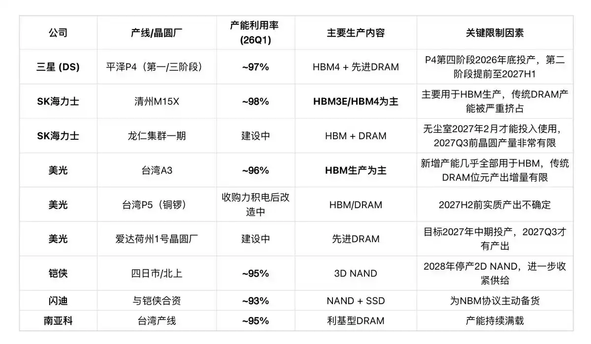
SemiAnalysis: "In 2026, almost all new wafer capacity will be concentrated in three wafer fabs: Samsung's P4, SK Hynix's M15X, and Micron's A3. Among them, both Micron's A3 and SK Hynix's M15X are expected to be primarily used for HBM production rather than traditional DRAM, which will limit the increment in wafer and bit output. For NAND, there is almost no actual wafer increment contribution in 2026, bit growth mainly relies on technology process upgrades."
This means: Even if capacity utilization rises from 95% to 98%, effective supply of traditional DRAM/NAND sees almost zero growth.
Indicator Two: Spot Price Index (As of May 8, 2026)
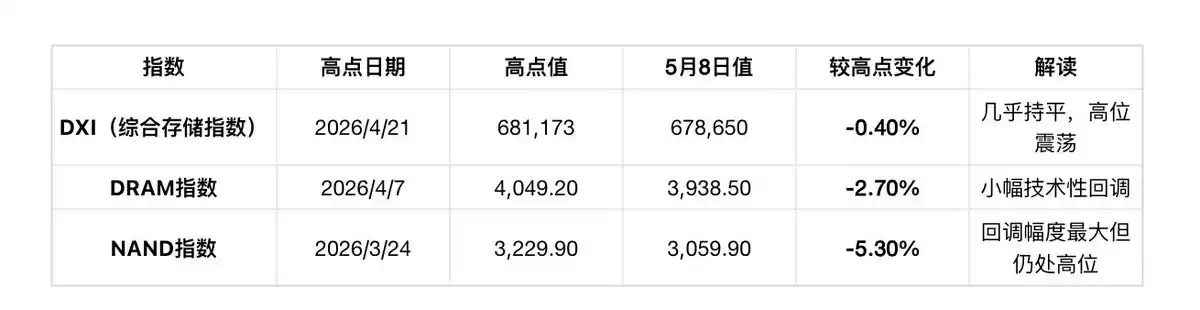
Data Source: Wind
Detailed DRAM Spot Prices (Daily, as of May 8):
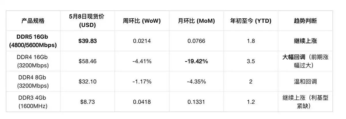
"Scissors Gap" Phenomenon between DDR4 and DDR5: DDR4 spot correction is due to previous excessive rise (large gap with contract prices), not demand collapse. DDR5 spot is still rising (WoW +2.14%), indicating AI server demand (mainly using DDR5) remains strong.
NAND Spot Prices (Weekly, as of April 27):
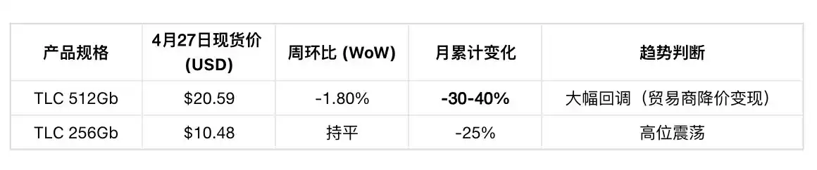
Three Reasons for NAND Spot Correction (China Merchants Securities): Previous excessive gains (doubled in 3 months) + Trader funding pressure for liquidity + Buyers generally observing. But contract prices completely unaffected: TrendForce expects Q2 NAND contract prices to still rise 70-75% QoQ.
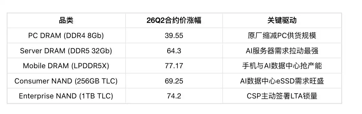
Indicator Three: Latest Contract Price Forecast (TrendForce May 2026)
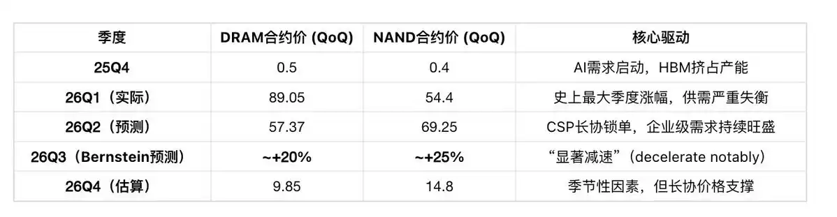
Sub-category Contract Price Forecast (Q2 2026):
Bernstein Mark Li (May 7, 2026): "Price increases are expected to decelerate notably into the third quarter. We expect the cycle to peak in mid-2027, with a gentle descent thereafter."
Indicator Four: Inventory Days (Latest Q1 2026)
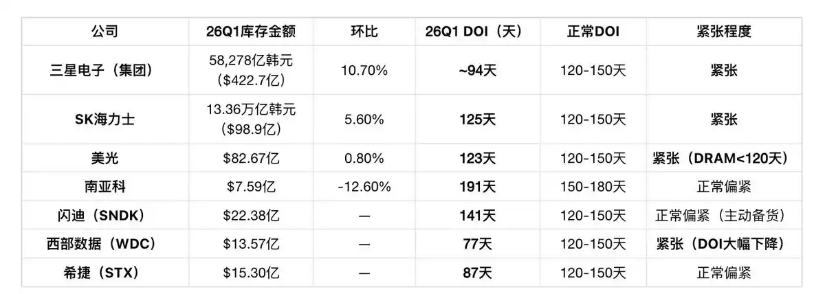
Four-layer inventory structure:
-
Manufacturers' finished goods inventory at 4-week level (SK Hynix finished goods only 28 days), zero buffer on supply side
-
Midstream module makers actively building inventory (Longsys + Silicon Motion + BIWIN combined 42.22 billion RMB, DOI 270-303 days), betting on continued price increases
-
Downstream customers signing LTAs and long-term agreements (SanDisk 5 NBMs covering over 1/3 of FY2027 bit output, Micron's first 5-year SCA)
-
HDD LTAs already extend to 2028-2029
Comprehensive Judgment: Where is the Cycle Currently Positioned?
Conclusion: The current (May 2026) storage supercycle is in the mid-phase of the upcycle (about 60-70% position), not near its end. Core arguments: Capacity utilization still has room to improve, contract prices still rising strongly, manufacturer inventory at strategic lows, long-term agreement lock-in proportion >50% significantly reduces risk of "demand collapse".