Musk is going to make his own chips. Not design—Tesla has been designing its own chips for seven years. This time, it's manufacturing. He announced an investment of approximately $25 billion to build a chip superfab named Terafab, targeting a 2nm process, with a monthly output of 100,000 wafers, integrating logic chips, memory, and advanced packaging within the same facility.
The reason behind this isn't complicated. Tesla's appetite for computing power has grown so large that external foundries can't keep up. Each generation of its autonomous driving chips sees a three to fivefold increase in computing power, with the Optimus robot and Robotaxi nearing mass production. Meanwhile, the world's most advanced process wafer capacity has already been snapped up by Apple, Qualcomm, and NVIDIA. Securing capacity through foundry contracts is just a stopgap measure; building their own fab is the endgame.
$25 billion. In other industries, this sum could buy an entire supply chain. In semiconductor manufacturing, it's not even enough to build a standard 2nm wafer fab.
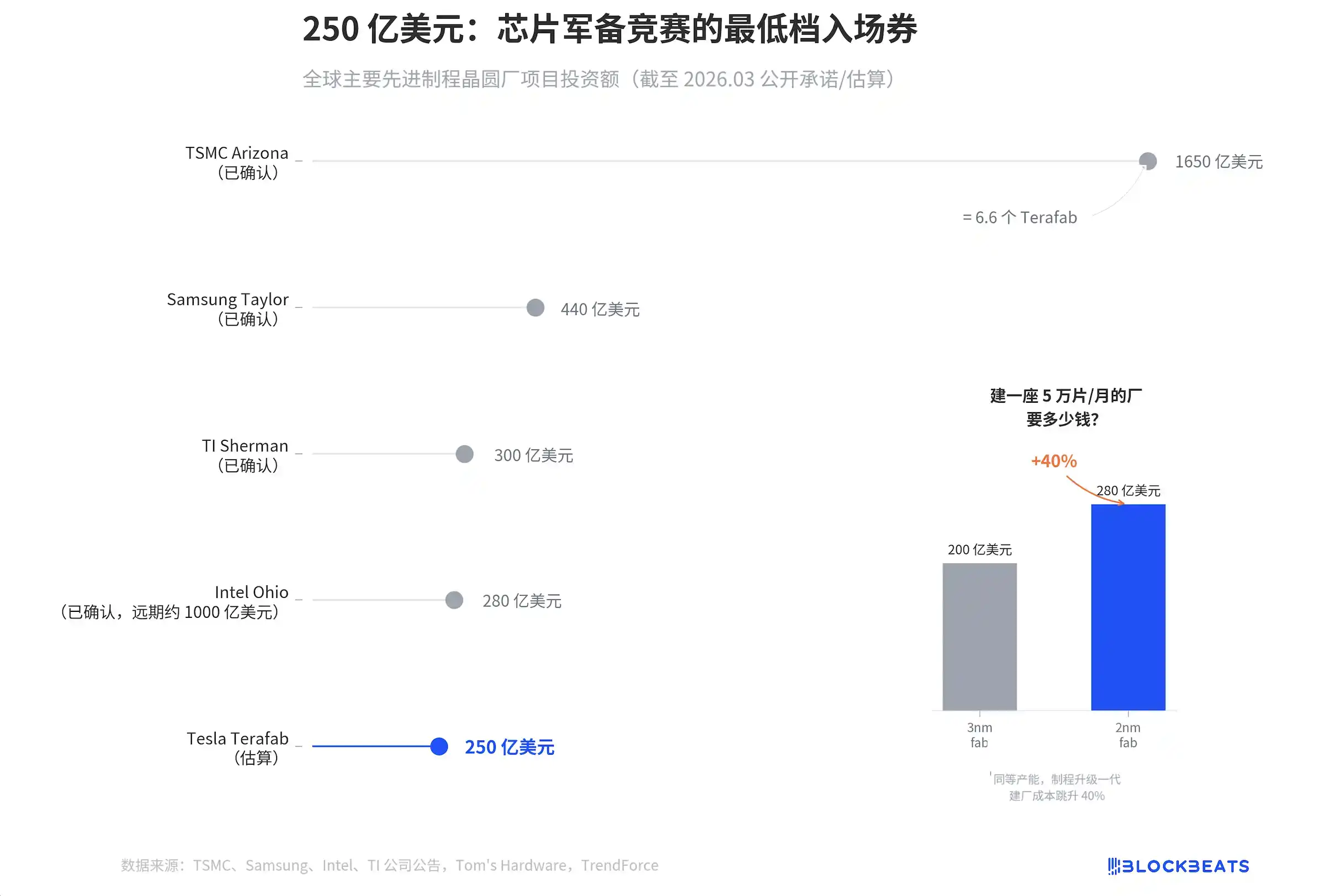
According to company announcements and industry media reports, the total investment for TSMC's Arizona campus is $165 billion, Samsung's Taylor fab is $44 billion, analog chip leader Texas Instruments' (TI) Sherman fab is $30 billion, and Intel's Ohio fab is $28 billion. Tesla ranks last. Furthermore, according to estimates by Tom's Hardware and other media outlets, its $25 billion is only an external推算 (calculation/speculation), and Musk himself has not confirmed an exact figure.
More crucially, look at the small chart on the right. According to estimates by industry research firms, building a fab with a monthly capacity of 50,000 wafers costs $20 billion for 3nm and $28 billion for 2nm. Moving from 3nm to 2nm, the construction cost jumps by 40%.
Tesla wants to achieve a monthly output of 100,000 2nm wafers with $25 billion. Based on industry benchmarks, a single 50,000 wafers/month 2nm fab alone costs $28 billion. Tesla aims to do the work of two fabs plus a packaging facility with less money than one standard fab. This isn't a budget; it's a wish list.
But what truly makes one gasp about Terafab isn't the money; it's the capacity target.
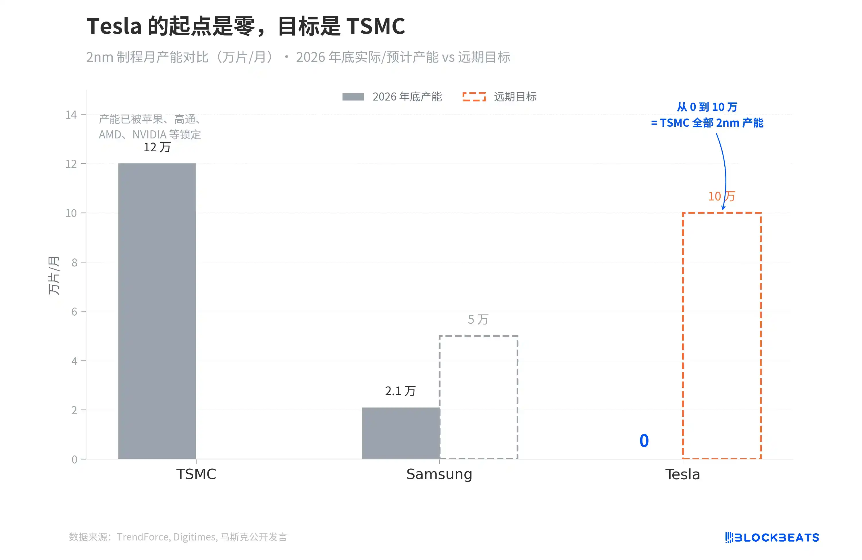
According to data from industry research firm TrendForce, TSMC's 2nm capacity is expected to be 100,000 to 130,000 wafers/month by the end of 2026, but this number has already been pre-booked by Apple, Qualcomm, AMD, and NVIDIA. According to a Digitimes report, Samsung's 2nm capacity is only 21,000 wafers/month, with a long-term target of 50,000.
Tesla's starting point is zero. The target is 100,000.
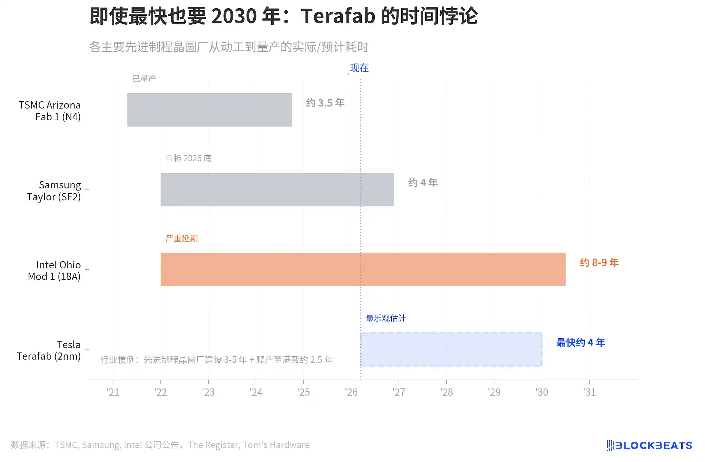
Going from 0 to 100,000 wafers/month equals starting from scratch to catch up with TSMC's entire global capacity for the most advanced process. TSMC started building its fab in Arizona in 2021 and took three and a half years to get its first 4nm fab into mass production. And TSMC has thirty years of manufacturing experience accumulated in Taiwan.
Tesla's manufacturing speed for cars did exceed everyone's expectations. But the margin for error in wafer manufacturing and vehicle manufacturing is not on the same scale. A flaw in a car can be recalled; a defect on a wafer means thousands of chips are scrapped.
To understand why Terafab is appearing in 2026, one must look at a longer timeline.
In 2019, the team led by Tesla's autonomous driving chip chief architect, Jim Keller, delivered HW3. This was Tesla's first fully self-developed autonomous driving chip, manufactured by Samsung on 14nm, with 144 TOPS. In 2023, HW4 upgraded to Samsung's 7nm, more than tripling the computing power. According to a TrendForce report, by AI5 in 2026, the process jumps to dual sourcing with 3nm and 2nm, with computing power直奔 (heading straight for) 2000 to 2500 TOPS, and it strips out the GPU and ISP entirely, optimizing the entire chip solely for transformer inference.
Each generation sees a three to fivefold performance increase. But the foundry strategy has also been evolving simultaneously. From HW3's "Samsung only," to AI5's "dual sourcing from TSMC and Samsung as a hedge," to AI6. According to TechCrunch and Bloomberg reports, for AI6, they directly signed a $16.5 billion long-term contract with Samsung to lock in capacity until 2033.
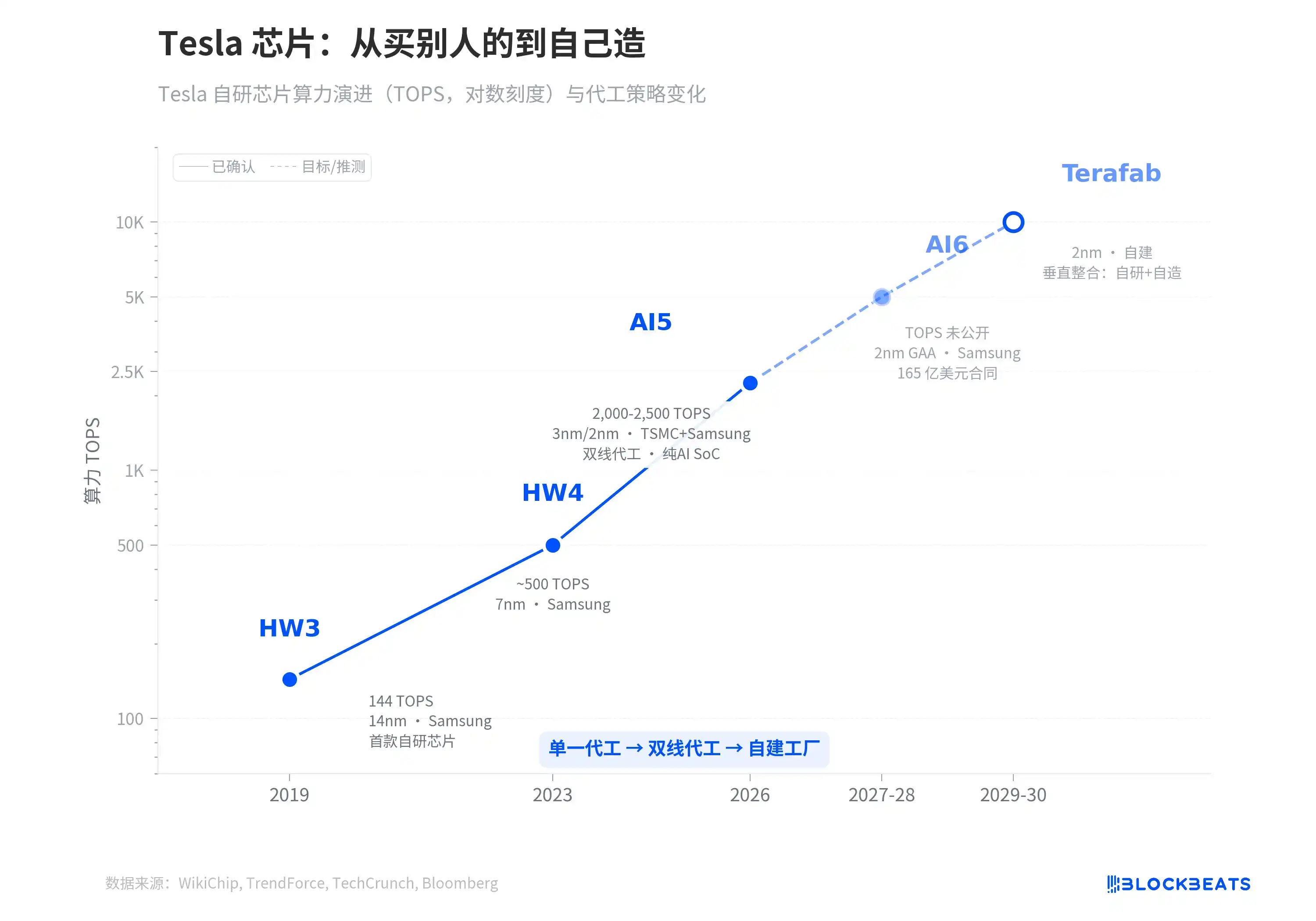
Terafab is the natural extension of this timeline. According to a Tom's Hardware report, last year Tesla's AI6 contract essentially saved Samsung's Taylor fab, that $44 billion factory which had been搁置 (shelved) due to "having no customers." When your chip demand is large enough to sustain someone else's wafer fab, the next question is, why not build your own.
The AI6 and Terafab nodes on the chart's dashed line segment are not labeled with specific TOPS because the specifications for these two generations have not been publicly released. But the trend direction is clear. The computing power curve of Tesla's chips is exponential, and the reliance on foundries has reached a point where it must be resolved.
The remaining question is time.
TSMC Arizona Fab 1 took about 3.5 years from groundbreaking to mass production, the industry's fastest record, but TSMC has thirty years of manufacturing积累 (accumulation). Samsung Taylor took about 4 years, pausing in the middle due to lack of customers. According to The Register, Intel Ohio is the worst, starting in 2022 and now delayed until 2030 or 2031.
Industry惯例 (convention) is 3 to 5 years for construction, plus another 2.5 years to ramp up to full capacity. Even giving Tesla TSMC's speed, Terafab would at the earliest start outputting wafers by the end of 2029.
And this恰好 (coincides) with Tesla's computing power bottleneck window. The dual sourcing for AI5 can last until 2027-2028, and the Samsung contract for AI6 covers until 2033. But if the mass production scale of the Optimus robot and Robotaxi explodes as Musk plans by 2029, external foundry capacity will likely be insufficient. Terafab doesn't need to produce chips in 2026; it needs to be ready by 2030.
Musk has also publicly discussed the possibility of cooperation with Intel. Intel has its most advanced 18A process (equivalent to the industry's 2nm level) and idle capacity desperately needing external customers; Tesla has clear chip demand and money. If this path materializes, Terafab wouldn't be starting from scratch alone, but a marriage of convenience where each gets what they need.
$25 billion doesn't buy much certainty in chip manufacturing. But it bought an entry ticket. A ticket that transforms Tesla from the biggest buyer of chips into a player in chip manufacturing. Looking back at this chart three years from now, it will either be the starting point of Tesla's vertical integration strategy, or Musk's most expensive pie-in-the-sky promise.