Glass Substrate Suddenly Accelerates

marsbitОпубликовано 2026-06-25Обновлено 2026-06-25

Введение

The adoption of glass substrates in the semiconductor industry is accelerating unexpectedly. Following collaboration announcements between BOE and Corning in late May, and earlier moves by Intel and TSMC, the market for related upstream companies has surged. Intel's "Glass Core Substrate" aims to replace the IC substrate between the circuit board and the chip, primarily addressing thermal warping issues in large AI chips. TSMC's focus is on replacing the expensive silicon interposer layer within the chip package to significantly reduce costs. While initially cautious, with timelines stretching towards 2030, progress has been dramatically pulled forward. Key drivers are NVIDIA, whose ever-larger GPUs like the upcoming Rubin make glass substrates a necessity, and the display panel industry. Companies like Innolux and BOE, leveraging their extensive experience and production lines in panel-grade glass substrates, are rapidly retooling for semiconductor packaging. Innolux has already established production lines and secured orders, while BOE has built pilot lines and is sampling customers. Although technical hurdles remain, such as advanced multi-layer glass processing and copper electroplating, the path to commercialization is now clearer. Large-scale adoption is estimated to begin by late 2027, marking glass substrates as a critical next step in supporting advancing AI computing power.

The AI computing power market is advancing in waves, with gains moving from one segment to another, and now it's the turn of glass substrates.

In late May, BOE announced a memorandum of cooperation with Corning on glass substrates, completely igniting the market.

Not only did its own steady stock price suddenly spike "like a jolt from a heartbeat monitor," with two consecutive trading days of limit-up gains, but upstream companies like Rainbow Display and Wufang Optoelectronics also hit the daily limit-up, Dier Laser's stock price reached a record high, and Vogo Optoelectronics has surged nearly 300% over the past two months.

Institutions have identified 2026 as the first year for commercial validation of glass substrates. Besides the cooperation between BOE and Corning, Intel announced successful mass production of glass core substrates in its latest server CPUs, and TSMC revealed the establishment of a glass substrate CoPoS packaging trial production line.

The two giants are pushing hard, setting the stage perfectly for the bullish atmosphere.

It must be said that the commercialization speed of glass substrates has already exceeded most people's expectations.

Replacing the "Board" in Chips

Intel and TSMC are the current top promoters of glass substrates, but the "glass substrates" they refer to are not exactly the same thing.

A chip is composed of various components mounted on carrier substrates, forming functional units. These functional units are then mounted on the next layer of carrier substrate, creating a larger functional unit, and so on, presenting a hierarchical structure.

For example, the most familiar circuit board is the bottom-most carrier substrate. Further up, there are core substrates, IC substrates, and so on.
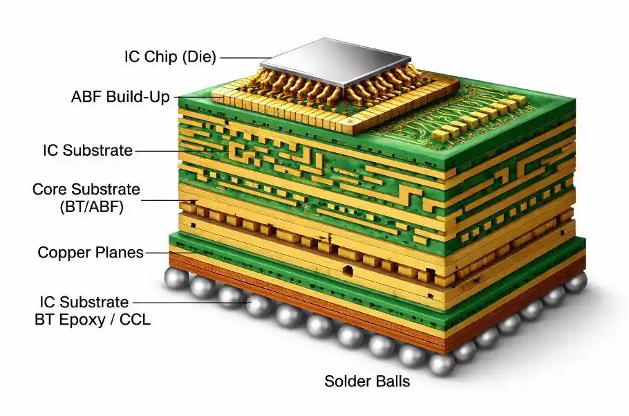
Different layers of "boards" inside a chip; Image source: IC Components

These carrier substrates were traditionally mostly made of materials like resin, fiberglass, copper foil, silicon, etc. As the name suggests, a glass substrate uses glass as the primary material for the substrate.

What Intel and TSMC aim to do is replace mainstream carrier substrates with glass substrates, but they are not targeting the same "board."

Intel's "advanced packaging glass substrate," officially named "Glass Core Substrate," replaces the IC substrate layer between the circuit board and the chip.
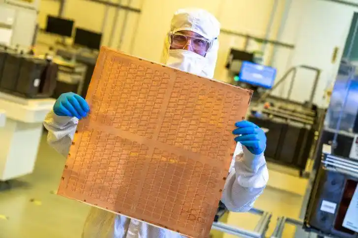
A test glass core substrate displayed by Intel

Currently, mainstream AI chips, including Nvidia GPUs, use substrates primarily made of ABF material. The biggest drawback is their tendency to warp and deform when heated. A one-meter-long ABF carrier substrate expands about 15 micrometers for every 1°C increase in temperature.

In contrast, the silicon chip placed on top of the ABF substrate shows almost no deformation when heated.

Thus, when heat is generated during chip operation, the bottom ABF substrate expands outward due to heat, while the upper silicon chip remains unchanged, causing the entire substrate to bend or "warp."

The larger the chip size, the more severe the warping becomes—imagine a credit card with all four corners curling up simultaneously. The consequences could be catastrophic.
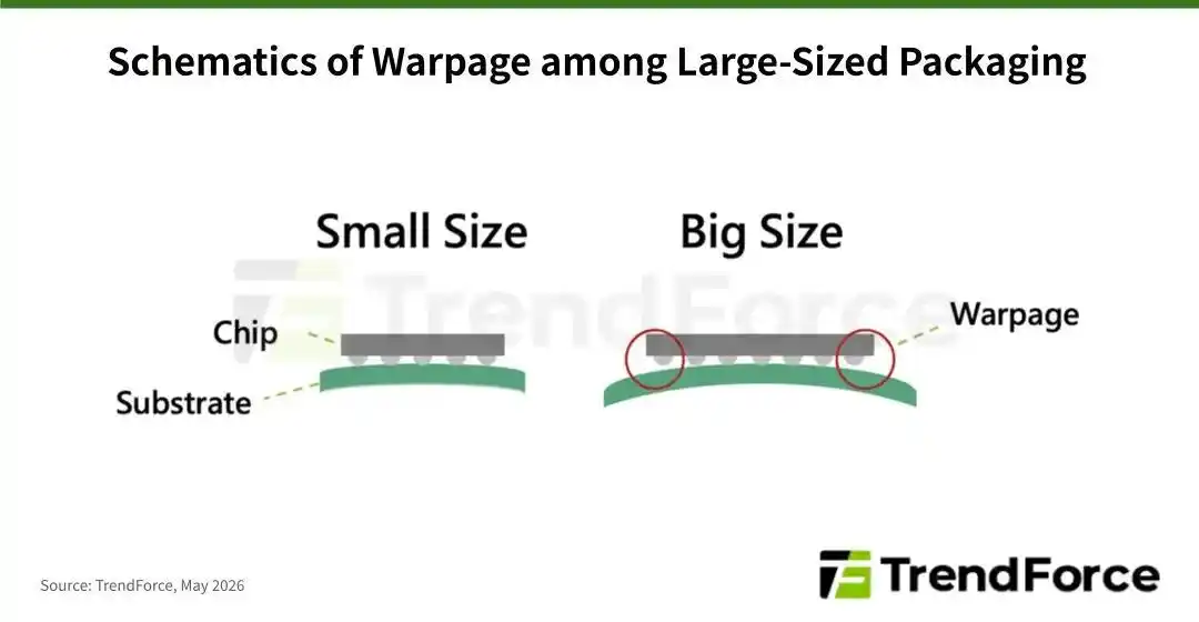
The larger the carrier substrate size, the more obvious the warping; Image source: TrendForce

This is why glass substrates are being considered. Due to their "heat resistance" being comparable to silicon chips, even if they deform at high temperatures, they can maintain synchronization with the silicon chip, effectively preventing warping.

Compared to Intel, TSMC wants to replace a carrier substrate located one layer higher—the bare die layer of the chip.

A GPU bare die consists of computing core units (CPU/GPU) and multiple HBM stacks, placed on a silicon interposer. This silicon interposer is the "board" TSMC most wants to replace.
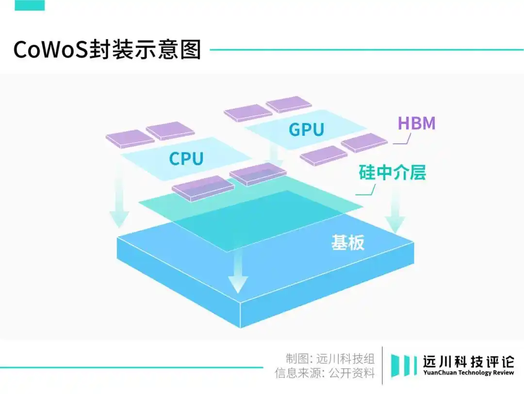
The manufacturing cost of a silicon interposer is extremely high, with a unit price exceeding $100 for a large-size silicon interposer [2]. For comparison, the A19 Pro chip in the iPhone 17 Pro Max costs only about $90 per unit for procurement.

Moreover, compared to these powerful computing SoCs for phones, the silicon interposer's main function is merely data transfer, akin to buying a scooter for the price of a sports car, which sounds even worse.

The size of the silicon interposer is directly related to the size of the AI chip and the number of HBM stacks used. As AI chips become larger and more HBM is used, the cost sinkhole for silicon interposers deepens.

For companies purchasing AI chips, it's like buying a car for $100,000 and having to spend an additional $50,000 on a license plate to drive it.

Replacing the silicon interposer with a glass substrate offers the biggest advantage: cost. For the same size, it costs less than half of the silicon counterpart [2].

The ideas from Intel and TSMC are both reasonable, but the implementation of new technology is never a simple order. Especially in the chip industry, new technology challenges not just the laws of physics.

Chip manufacturing is humanity's most complex activity to date, having solidified over the past half-century into an extremely strict set of rules. The upstream and downstream segments have meticulously built a standardized system where everything is tightly interlocked; a small adjustment can affect everything.

Even the slightest adjustment may lead to changes or complete overhauls in upstream equipment and materials.

Hence, while giants talk boldly about innovation, their actions remain conservative and cautious.

Intel proposed the glass core substrate concept in 2023, with mass production vaguely scheduled for sometime between 2026 and 2030. TSMC has been secretive about its CoPoS plan, only recently revealing for the first time that it would take 2-3 years to scale up to a certain size.

However, a few big hands have forcefully yanked the progress bar forward by a large margin.

Who is Pulling the Progress Bar?

The first big hand is Nvidia.

Just a few months after Intel announced the glass core substrate, Morgan Stanley released a report predicting that GB200 "might" use glass substrates for packaging.

This report was once overinterpreted as "Nvidia officially announced GB200 will use glass substrates," causing another surge in related concept stocks.

Putting the misunderstanding aside, the fact that an unsupported speculation could have such strong persuasive power is because, in the public's perception, Nvidia indeed has the greatest motivation to push glass substrate adoption.

Nine out of ten AI computing power chips are Nvidia GPUs. Bearing the weight of exponentially increasing computing demands, each GPU generation strives to pack more transistors, leading to larger and larger GPUs.

The B200's area is nearly double that of its predecessor, the H100, almost 10 times the size of Apple's M2 Ultra chip, roughly half the size of a bank card, already pushing the warping limits of ordinary IC substrates.

The upcoming Rubin, set for mass production in the second half of the year, is even larger than the B200. Changing materials is not an option but a necessity.
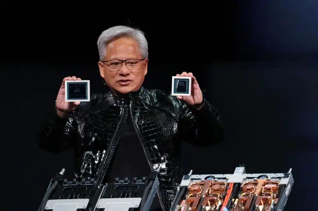
Jensen Huang holding B200 (left) and H100 (right)

In March this year, Nvidia announced a full shift to glass substrates, with Rubin leading the trial, fast-forwarding the commercialization timeline to the end of this year.

With Nvidia's big hand pulling from the front, an unexpected big hand is pushing from behind. It's not from the upstream chip industry, but from a neighboring sibling industry—display panels.

Before being used in chip packaging, the largest downstream application for glass substrates was display panels.

A display panel has a sandwich structure internally, with the two "slices of bread" being glass substrates—one controlling brightness, the other controlling color.
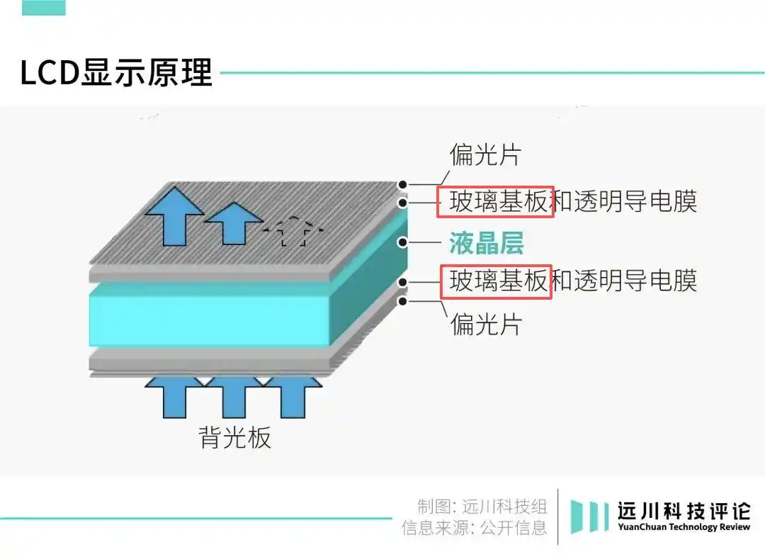
Glass substrates in an LCD panel

The precision processing technologies and equipment used here have extremely high overlap with those needed for glass substrates in chips. Exaggerating a bit, high-end production lines can be modified for use.

Therefore, regarding glass substrate implementation, the most enthusiastic are actually brothers from the panel industry.

For example, Taiwan's major panel maker Innolux plotted a transition to chip packaging as early as 2019.

With a global panel price war raging fiercely, Innolux, seeing it couldn't hold out, accepted an olive branch from Taiwan's Industrial Technology Research Institute (ITRI) to jointly develop glass substrate-based chip packaging technology, modifying its own panel production lines.

By the time Intel announced glass substrate technology in 2023, Innolux had already built the world's first FOPLP packaging production line converted from a panel line.

The following year, it secured major orders from chip giants NXP and STMicroelectronics, and sold an idle 5.5-generation panel line at a high price to TSMC to alleviate the latter's shortage of advanced packaging capacity.

By early this year, Innolux's FOPLP advanced packaging line had increased monthly production tenfold to tens of millions, not only firmly embracing TSMC's leg but reportedly also entering SpaceX's Starlink supply chain.

Taiwan's panel makers work fiercely hard, and progress on the mainland side is equally rapid.

BOE began researching and developing glass substrates in 2020, invested nearly 1 billion yuan in building a pilot line in 2024, and achieved fully automated equipment operation in the first half of this year [4].

It has already started sending samples to customers for testing and validation. The cooperation with Corning in May was to lock in future years of upstream specialty glass supply, with large-scale mass production imminent.

Mainland China holds over 60% of global panel capacity, especially in high-generation panels with the world's most mature and highly automated production lines. A bigger advantage lies in having a complete upstream industry chain for support.

Several companies currently of most interest in the secondary market, such as Dier Laser, Han's Laser, and Delong Laser, are upstream manufacturers of TGV (Through Glass Via) laser microvia equipment. Vogo Optoelectronics is midstream, handling glass substrate processing.

Beyond Chinese manufacturers, Korea's Samsung Electro-Mechanics, LG Innotek, Japan's Dainippon Printing, and Nippon Electric Glass are all active proponents of glass substrates—familiar faces from the panel wars.

With downstream demand secured by big spenders and upstream sibling industries providing warm support, glass substrates have quickly progressed from being seriously criticized as "concept hype" to the "eve of mass production." Securities firms have changed their cautious stance, drawing bigger and bigger pies.

Objectively speaking, there are still several technical hurdles to overcome before glass substrates achieve large-scale implementation.

For example, the core material—specialty glass—currently only Corning can process up to 11 layers without cracking, while the domestic supply chain can manage at most 3-4 layers [5]. Other issues include insufficient copper electroplating equipment and processes [5].

According to industry chain estimates, the earliest large-scale volume production for glass substrates will likely be by the end of 2027.

The end of computing power is electricity, but before reaching that end, the industry chain must cross another hurdle—perhaps one more glass substrate.

References

[1] Research on Warpage of 2.5D CoWoS Packaging Based on Glass Substrate, Shi Hangbo, Wang Xu, Fan Jilei, et al.

[2] Large Silicon Interposer Unit Price Exceeds $100, Accounting for Half the Cost; How Can AI Computing Chips Break Through the Packaging Cost Bottleneck? Yue Tou Gu

[3] Complete Breakdown of TGV Glass Via: After Intel's Glass Substrate Entry, Understanding the Hard Barriers, 2027 Mass Production Countdown, and Taiwan Supply Chain Investment Map, Sinopac Securities

[4] BOE: Glass Substrate Packaging Carrier Pilot Line Operational, Design Capacity 1000 Sheets/Month, Future Semiconductor

[5] Glass Substrate Industry Exchange, Summary Research Report

This article is from the WeChat public account "Yuanchuan Technology Review" (ID: kechuangych), author: He Lüheng, editor: Li Motian

Трендовые криптовалюты

Связанные с этим вопросы

QWhat are the two main applications of glass substrates in the chip industry, as promoted by Intel and TSMC respectively?

AIntel promotes the use of 'Glass Core Substrate' to replace the IC substrate layer (between the circuit board and the chip). TSMC aims to use glass substrates to replace the silicon interposer layer (within the chip's bare die layer).

QWhy is the transition to glass substrates becoming increasingly necessary for high-performance AI chips like NVIDIA's GPUs?

AAs AI GPUs become larger (e.g., B200, Rubin) to pack more transistors, the traditional organic ABF substrates are prone to warping due to heat. Glass substrates have thermal properties similar to silicon, preventing this warping and enabling larger chip designs.

QWhich non-semiconductor industry is playing a significant role in accelerating the adoption of glass substrates for chip packaging, and why?

AThe display panel industry is a key accelerator. Companies like Innolux and BOE are repurposing their mature, high-precision panel manufacturing lines and expertise for glass substrate processing, providing ready-made production capacity and supply chain support.

QWhat is the primary benefit for TSMC in replacing silicon interposers with glass substrates in its CoWoS packaging?

AThe primary benefit is significant cost reduction. Large silicon interposers are extremely expensive (over $100 each), while similarly sized glass substrates are estimated to cost less than half that amount.

QAccording to the article, what are some of the key technical challenges that still need to be overcome before glass substrates can achieve mass adoption?

AKey challenges include: 1) Developing special glass materials that can withstand multiple layers (e.g., 11+) of processing without breaking; 2) Improving copper electroplating equipment and processes for creating high-quality interconnects within the glass substrate.

Похожее

После трёх кварталов падения: получится ли у крипторынка стабилизироваться в третьем квартале?

Криптовалютный рынок пережил худший квартал с 2022 года, общая капитализация упала на 12,6% до $2,1 трлн, а дневные объемы торгов снизились на 20,9%. Впервые за три года сократилась и капитализация стейблкоинов. Основные факторы спада — отток средств из биткоин-ETF, распродажа биткоинов корпоративным казначейством Strategy и ужесточение монетарной политики ФРС. Второй квартал завершился чистым оттоком $46,7 млрд из ETF, при этом в июне отток достиг рекордных $45 млрд. Ключевым событием третьего квартала станет заседание ФРС 28–29 июля. Мягкий сигнал может поддержать биткоин в диапазоне $68 000–84 000 и вернуть приток в ETF, тогда как жесткая риторика способна сместить торговый диапазон к $50 000–56 000. Законодательная неопределенность также давит на рынок: прогресс по закону CLARITY Act, определяющему регуляторные границы, замедлился, и вероятность его принятия в 2026 году упала до 40–45%. Несмотря на общий спад, два сегмента показали рост: объемы на рынках предсказаний выросли на 48,7%, а торговля токенизированными коллекционными предметами увеличилась на 143%. Сектор RWA продолжает стабильно развиваться, достигнув $28,1 млрд. Рынок, вероятно, миновал фазу острой распродажи, но для устойчивого восстановления необходимы ясность от ФРС и регуляторный прогресс.

marsbitВчера 08:38

После трёх кварталов падения: получится ли у крипторынка стабилизироваться в третьем квартале?

marsbitВчера 08:38

BIT Торговые часы: BTC по-прежнему под давлением 200 EMA на недельном графике, после отскока возможен перезапуск нисходящего движения; секторы хранения данных и полупроводников, выросшие ночью, начали падение в вечерней сессии

**Краткий обзор рынка: BTC под давлением, коррекция на рынке акций, внимание к данным и событиям** Рынок криптовалют демонстрирует осторожное восстановление. Bitcoin торгуется около $66 000, сталкиваясь со значительным сопротивлением в районе $68 000, где сосредоточены объемные "застрявшие" позиции. Ключевые технические уровни — 200-недельная скользящая средняя (~$63 333) и 200-недельная EMA (~$68 328). Аналитики отмечают низкую ликвидность, характерную для летнего периода. На фондовом рынке после сильного роста во вторник наблюдается коррекция. Фьючерсы на основные индексы США снижаются. Акции полупроводниковой и памяти, которые резко выросли накануне, падают в ночных торгах. Исключением стал SMCI, который вырос более чем на 15% после оптимистичного прогноза. На общий настрой негативно влияют рост цен на нефть (более $91 за баррель Brent) и доходности государственных облигаций США (10-летние — около 4,64%), что возрождает инфляционные опасения. Азиатские рынки показали нестабильную динамику. Индекс KOSPI в Корее вырос на 0,74%, а японский Nikkei 225 снизился на 0,18%. Основной риск для региона — ослабление японской иены до минимумов с 1986 года, что повышает вероятность вмешательства властей. **Ключевые события для наблюдения:** * **24 июля:** Финансовые отчеты Alphabet (Google), Tesla, IBM. Событие AMD, посвященное ИИ. * **25 июля:** Решение по процентной ставке ЕЦБ и пресс-конференция Кристин Лагард. Финансовые отчеты Intel, American Airlines, Honeywell и других. Данные по числу первичных заявок на пособие по безработице в США.

marsbitВчера 08:30

BIT Торговые часы: BTC по-прежнему под давлением 200 EMA на недельном графике, после отскока возможен перезапуск нисходящего движения; секторы хранения данных и полупроводников, выросшие ночью, начали падение в вечерней сессии

marsbitВчера 08:30

Бывший глава CFTC и президент Circle Тарберт: призывает к долгосрочной стратегии, но сам выводит $30 млн

Бывший председатель CFTC и президент Circle Хит Тарберт, публично пропагандируя долгосрочное видение компании для инвесторов на фоне падения акций на 70% с пиковых значений, сам активно распродавал свои акции CRCL. С момента IPO Circle он по плану 10b5-1 продал более 360 тысяч акций, выручив около 30 миллионов долларов, и при этом ни разу не докупал акции на открытом рынке. Эта разница между его публичными заявлениями и личными действиями вызвала критику. Карьера Тарберта демонстрирует классическое использование «вращающейся двери» между регулирующими органами и частным сектором. Уйдя с поста председателя CFTC в 2021 году, через 27 дней он занял должность главного юрисконсульта в маркет-мейкере Citadel Securities, который в тот момент находился под пристальным вниманием из-за скандала с акциями GameStop. Позже, уже работая в Citadel, Тарберт выступал за расширение полномочий CFTC на крипторынок, в то время как его работодатель планировал выход на этот рынок. В 2023 году Тарберт присоединился к Circle, где его опыт и связи сыграли ключевую роль в успешном проведении IPO компании в 2025 году. Однако его последующие массовые продажи акций, совпавшие с падением котировок и его же призывами к долгосрочным инвестициям, ставят под сомнение искренность его уверенности в будущем компании. Критики видят в его карьере образец превращения регуляторного опыта и политических связей в личную выгоду, в то время как риски несут обычные инвесторы, верящие его нарративам.

marsbitВчера 08:07

Бывший глава CFTC и президент Circle Тарберт: призывает к долгосрочной стратегии, но сам выводит $30 млн

marsbitВчера 08:07

Gate Research: Взлет «уолл-стритизации» криптофинансовых продуктов — это конкуренция или интеграция?

**Аналитический обзор Gate Research Institute: Волна "уолл-стритизации" криптофинансовых продуктов — конкуренция или интеграция?** Создание биткоина в 2009 году было ответом на финансовый кризис и стремлением построить децентрализованную систему без доверенных посредников. Однако к 2026 году значительная часть биткоинов (около 7,14%) хранится через ETF таких гигантов, как BlackRock. Это символизирует глубокую интеграцию традиционных финансов (TradFi) и крипторынка. С появлением биткоин-ETF, фьючерсов, RWA (токенизированных реальных активов) и государственных облигаций на блокчейне, традиционные институты получают всё больше влияния на выпуск, ценообразование, кастодию и дистрибуцию криптоактивов. Однако это не одностороннее поглощение, а взаимодополняющая конвергенция. Криптосфера приносит TradFi глобальную 24/7 ликвидность и программируемость, а TradFi предоставляет криптосфере регулируемые каналы, институциональное доверие и массовый доступ. Яркий пример — две противоположные, но ведущие к одной цели траектории: * **Путь А:** Криптобиржи, такие как Gate, начинают с токенизированных акций и CFD, а затем напрямую подключаются к инфраструктуре традиционных брокеров, предлагая реальную торговлю акциями США, Гонконга и Кореи за стейблкоины. * **Путь Б:** Традиционные брокеры, такие как Robinhood, интегрируют криптоактивы, а затем создают собственные Layer 2 для токенизации своих акций, стремясь к круглосуточной торговле. Обе стратегии нацелены на создание **универсального финансового аккаунта будущего** — единой точки доступа к акциям, криптовалютам, ETF, токенизированным облигациям и другим активам. Ключевой конкурентной борьбой становится не между CEX и брокерами, а между этими "супераккаунтами". Параллельно, слой RWA и токенизированных гособлигаций растёт даже на медвежьем рынке, становясь "прослойкой" для объединения капиталов. Хотя этот рынок (около $150 млрд токенизированных казначейских облигаций) ещё мал по сравнению с традиционным ($30 трлн), он демонстрирует устойчивый структурный тренд, привлекающий крупнейшие финансовые институты (JPMorgan, DTCC и др.). **Вывод:** "Уолл-стритизация" — это не поражение идеалов децентрализации, а формирование новой гибридной модели. Децентрализованные протоколы продолжают работать на базовом уровне, в то время как на уровне приложений и пользовательского опыта формируется более эффективный, глобальный и свободный объединённый рынок капитала, где активы TradFi и DeFi торгуются бок о бок в одном интерфейсе. Уолл-стрит не завоевала криптосферу, а криптосфера не обошла Уолл-стрит — они совместно строят новые финансовые рельсы.

marsbitВчера 08:04

Gate Research: Взлет «уолл-стритизации» криптофинансовых продуктов — это конкуренция или интеграция?

marsbitВчера 08:04

S&P Dow Jones и Pantera выпускают криптоиндекс, биткоин оставлен за бортом из-за «отсутствия прибыли»

Стандард энд Пурс (S&P Dow Jones Indices) совместно с Pantera Capital запускает индекс S&P Pantera Digital Asset Index. Новый индекс включает 18 токенов, но исключает биткоин, XRP и мем-токены. Критерием отбора послужила «финансовая жизнеспособность», по аналогии с S&P 500: протокол должен демонстрировать положительный доход в течение нескольких кварталов и распределять стоимость среди держателей токенов. Это первое применение фундаментального подхода к оценке криптоактивов со стороны крупнейшего в мире провайдера индексов. В первую пятерку активов вошли Ethereum (ETH), BNB, Solana (SOL), TRON (TRX) и Hyperliquid (HYPE). Pantera отмечает, что совокупный годовой доход всех протоколов индекса превышает $30 млрд. Биткоин был исключен по трем причинам: он рассматривается как монетарный актив, доступный через отдельные ETF; он не генерирует доход протокола; а смешивание его в индексе с доходными активами затрудняет фундаментальный анализ для институциональных инвесторов. Пока индекс является эталонным, но Pantera ведет переговоры о создании на его основе ETF и других инвестиционных продуктов. Компания также отмечает значительный разрыв на рынке: многие институциональные инвесторы готовы к аллокации в криптоактивы, но им не хватает структурированных продуктов, фокусирующихся на активах с реальной экономической деятельностью.

marsbitВчера 08:02

S&P Dow Jones и Pantera выпускают криптоиндекс, биткоин оставлен за бортом из-за «отсутствия прибыли»

marsbitВчера 08:02

Торговля

Спот

Популярные статьи

Как купить WAVES

Добро пожаловать на HTX.com! Мы сделали приобретение Waves (WAVES) простым и удобным. Следуйте нашему пошаговому руководству и отправляйтесь в свое крипто-путешествие.Шаг 1: Создайте аккаунт на HTXИспользуйте свой адрес электронной почты или номер телефона, чтобы зарегистрироваться и бесплатно создать аккаунт на HTX. Пройдите удобную регистрацию и откройте для себя весь функционал.Создать аккаунтШаг 2: Перейдите в Купить криптовалюту и выберите свой способ оплатыКредитная/Дебетовая Карта: Используйте свою карту Visa или Mastercard для мгновенной покупки Waves (WAVES).Баланс: Используйте средства с баланса вашего аккаунта HTX для простой торговли.Третьи Лица: Мы добавили популярные способы оплаты, такие как Google Pay и Apple Pay, для повышения удобства.P2P: Торгуйте напрямую с другими пользователями на HTX.Внебиржевая Торговля (OTC): Мы предлагаем индивидуальные услуги и конкурентоспособные обменные курсы для трейдеров.Шаг 3: Хранение Waves (WAVES)После приобретения вами Waves (WAVES) храните их в своем аккаунте на HTX. В качестве альтернативы вы можете отправить их куда-либо с помощью перевода в блокчейне или использовать для торговли с другими криптовалютами.Шаг 4: Торговля Waves (WAVES)С легкостью торгуйте Waves (WAVES) на спотовом рынке HTX. Просто зайдите в свой аккаунт, выберите торговую пару, совершайте сделки и следите за ними в режиме реального времени. Мы предлагаем удобный интерфейс как для начинающих, так и для опытных трейдеров.

627 просмотров всегоОпубликовано 2024.03.29Обновлено 2026.06.02

Как купить WAVES

Обсуждения

Добро пожаловать в Сообщество HTX. Здесь вы сможете быть в курсе последних новостей о развитии платформы и получить доступ к профессиональной аналитической информации о рынке. Мнения пользователей о цене на WAVES (WAVES) представлены ниже.

活动图片