18 Months, Over 50x Surge: KIOXIA's Epic Comeback

marsbitPublié le 2026-06-23Dernière mise à jour le 2026-06-23

Résumé

KIOXIA, a NAND flash memory giant, staged a dramatic comeback driven by AI demand. After a period of significant losses, a failed merger, and missed HBM opportunities, its 2024 IPO began modestly. However, fueled by explosive demand for AI data storage, its stock price skyrocketed over 50 times within 18 months, making it Japan's most valuable company, surpassing Toyota. Its Q1 FY2026 profit guidance soared 30-fold year-over-year, with 2026 NAND capacity already sold out. Key to its success is its 3D NAND technology, BiCS FLASH. As the inventor of NAND, KIOXIA advanced its technology through generations, reaching over 200 layers by 2023. Key innovations include CBA (CMOS directly Bonded to Array), which separately manufactures control circuits and memory arrays for better performance, and OPS (On Pitch Select Gate) to increase density. The company is now developing high-capacity packages like an 8TB solution stacking 32 dies. Looking beyond NAND, KIOXIA is exploring 3D DRAM with its OCTRAM technology, using oxide semiconductor transistors for ultra-low leakage to reduce power consumption. This fundamental research differs from HBM and represents a long-term bet to extend its 3D expertise from NAND into future DRAM architectures. KIOXIA's story highlights how technological assets and shifting market cycles can rapidly transform a company's fortunes. While questions remain about sustaining growth beyond the current AI boom, its resurgence demonstrates that in semiconductors,...

Author: Du Qin DQ

Previously, we have deeply analyzed this flash memory giant's regrettable trough period in another article: burdened by the past glory of Toshiba Memory but 'born at the wrong time'; cold-shouldered by the capital markets, leading to a last-minute IPO setback; suffering consecutive huge losses in an industry downturn, and unfortunately missing out on the enormous opportunity of HBM, with even its attempt to seek refuge through a merger with Western Digital falling through... At that time, KIOXIA seemed to have become a 'hot potato' in the eyes of outsiders amid the semiconductor industry reshuffle.

However, just over a year later, KIOXIA staged a comeback that can be described as epic. Driven by the frenzy of AI large models, the market logic for storage underwent a fundamental shift. KIOXIA not only successfully reversed its fortunes but also achieved a dual explosion in both capital markets and technology.
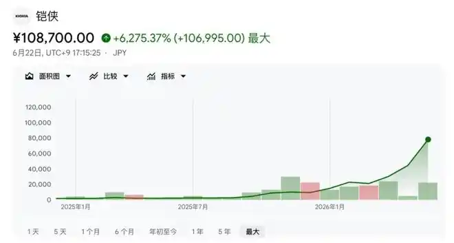
KIOXIA's stock price trend since listing

The Super Myth in the Capital Markets

KIOXIA successfully listed on the Tokyo Stock Exchange at the end of 2024, with its initial market capitalization hovering around only 800 billion yen (approximately $50 billion). However, with the comprehensive explosion of AI storage demand, KIOXIA performed an epic reversal in the 18 months following its listing: its stock price skyrocketed over 50 times within 18 months, rising 8-fold in 2026 alone.

Currently, KIOXIA's market capitalization has exceeded 51 trillion yen (approximately 481 trillion Korean won), repeatedly surpassing Toyota Motor, the symbol of Japanese manufacturing, to become the highest-valued company on the Japanese stock market.

According to KIOXIA's Q1 FY2026 (April–June) earnings forecast, its quarterly operating profit is expected to reach as high as 1.3 trillion yen (approximately $81 billion), a staggering increase of nearly 30 times year-over-year; the quarterly net profit guidance is 869 billion yen, a 48-fold increase year-over-year. The performance of a single quarter surpassed the full-year net profit forecast for FY2025.

As major customers scrambled to sign long-term supply contracts, KIOXIA's 2026 NAND capacity has been completely sold out, and the supply-demand imbalance is expected to persist until 2027. The market anticipates KIOXIA's operating profit margin this year to exceed 60%, setting a record for the highest profitability level in the global memory industry. Furthermore, with market expectations for shareholders to receive returns such as stock splits and dividends, its target stock price is hoped to rise to 200,000 yen.

This wave of soaring value has delivered investment returns beyond imagination to parent company Bain Capital, which held on during the downturn, and indirect major shareholder SK Hynix.

According to the Financial Times, the AI boom has made Bain's 2018 acquisition of Toshiba Memory (now KIOXIA) one of the most profitable private equity deals in history. Bain Capital has realized profits by selling most of its shares, with returns exceeding $150 billion, a near 20x return on investment. Its flagship private equity fund is estimated to have gained over $8 billion in profit.

SK Hynix invested a total of 395 billion yen (approximately 3.9 trillion Korean won at the time) in Toshiba Memory in 2018 through a consortium involving Korea, the US, and Japan, among other forms. Currently, this consortium still holds an 18% stake in KIOXIA. With the surge in KIOXIA's stock price, SK Hynix has seen enormous paper gains, and the market expects the consortium's eventual total profit to far exceed $70 billion.

The former 'hot potato' instantly transformed into a 'super ATM'.

In the past, the benefits of artificial intelligence were mainly concentrated in GPU and HBM companies like NVIDIA and SK Hynix. HBM was the star on the AI training side, while NAND became a scarce resource in AI inference, model storage, data lakes, enterprise SSDs, and nearline storage. The market expects KIOXIA's net profit for FY2027 to reach 2.8389 trillion yen, a 5.1-fold increase compared to the previous year.

3D NAND, The Foundation of KIOXIA's Existence

KIOXIA invented NAND flash memory over 35 years ago. In 2007, KIOXIA introduced BiCS FLASH 3D flash memory, a 3D flash memory technology system centered around vertical stacking, lateral scaling, wafer bonding, select gate optimization, and advanced packaging.

The basic idea of 3D NAND is: unlike 2D NAND, which only shrinks cells on a plane, it stacks memory cells vertically like building a skyscraper. KIOXIA's explanation is vivid: originally it was one floor with limited land area; 3D NAND is equivalent to turning a one-story building into a multi-story apartment, accommodating more 'residents' on the same area.

The core of BiCS FLASH is its batch processing technology. Its general process logic is: first, alternately stack plate-like electrodes and insulating layers; then drill a large number of holes along the vertical direction in one go; next, fill the holes with charge storage films and pillar-like electrodes; the intersection of the plate-like electrode and pillar-like electrode forms a memory cell. This shows that KIOXIA's BiCS FLASH is not the traditional 'create memory cells separately for each added layer,' but rather stacks the structure first, then forms memory cells by 'punching and plugging' through multiple layers at once. Therefore, when the number of layers increases, the manufacturing cost does not rise completely linearly, improving the economic viability of continued stacking for 3D NAND.

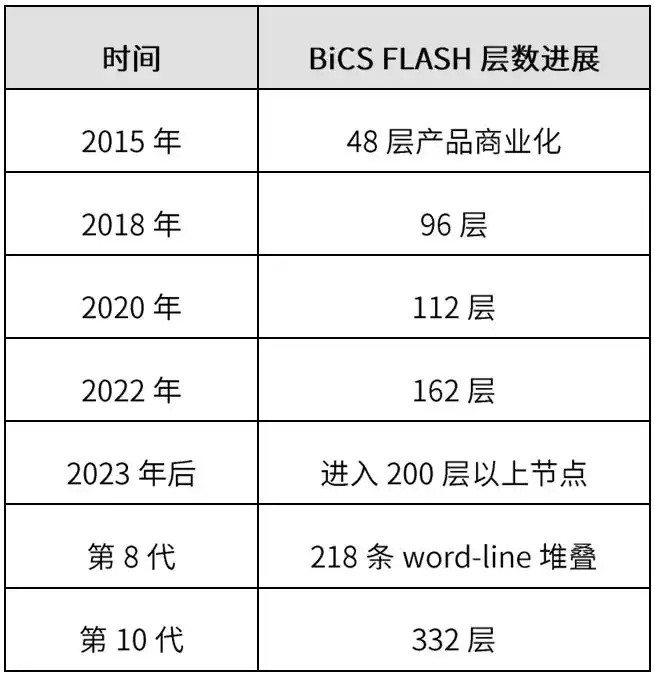
KIOXIA's officially disclosed commercialization timeline for BiCS FLASH is roughly as follows: BiCS FLASH products achieved commercialization with 48 layers in 2015, then progressed to 96 layers, 112 layers, 162 layers; as of March 2023, stacking of over 200 layers has been achieved.

Among these, the 8th-generation BiCS FLASH is a key milestone. KIOXIA states that the 8th-generation product uses 218 word-line stacks, achieves a storage density of 18.3Gb/mm² for the 1Tb TLC product, and supports a 3.2Gbps external data transfer speed, 40μs read time, and 205MB/s programming throughput.

KIOXIA's 8th-generation BiCS FLASH not only jumped from 162 layers to 218 layers but also introduced two key technologies:

CBA (CMOS directly Bonded to Array): CBA can be understood as manufacturing the peripheral CMOS control circuit and the memory array separately, followed by wafer bonding. In the past, CMOS circuits and the memory array were manufactured on the same wafer. However, the optimal process conditions for both are not identical: the memory array may require processes better suited for charge storage and stacked structures, while CMOS circuits focus more on logic control, electrical performance, and speed. Manufacturing them on the same wafer forces compromises.

CBA's approach is: manufacture the CMOS wafer separately, manufacture the memory array wafer separately, optimize the processes for each independently, and finally bond them together with high precision. The benefits are: improved bit density, increased NAND I/O speed, allowing the memory array to use high-temperature processes previously limited by CMOS constraints, and reduced electrical interference between adjacent memory cells.

OPS (On Pitch Select Gate): OPS solves the problem of wasted space within the memory array. In traditional structures, there exist 'dummy' areas between memory cells that are not used for data storage. These areas do not directly contribute to capacity but occupy area. KIOXIA's OPS technology, by rearranging select gates and insulating isolation structures, reduces or eliminates these ineffective areas, allowing more effective memory cells to be placed in the same area. KIOXIA's official explanation states that OPS removes unnecessary dummy regions, enabling more actual memory cells to be placed in the same space, significantly improving storage density.
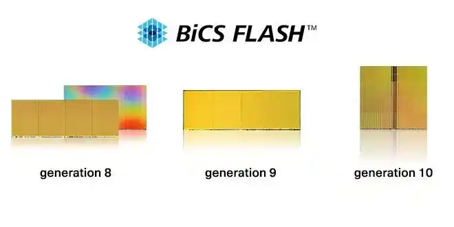
The 9th-generation BiCS FLASH primarily targets 512Gb and 1Tb TLC products, positioned to support applications in the mid-to-low capacity range that require high performance and low power consumption. It continues to use CBA and OPS technologies to improve production efficiency and provide more advanced flash memory solutions. The 9th generation does not follow the route of increasing layer count but emphasizes the balance between performance, power consumption, cost, and production efficiency.

The 10th-generation BiCS FLASH clearly leans more towards future high-capacity, high-performance demands. KIOXIA states that the 10th-generation product uses the same CMOS technology as the 9th generation while increasing the number of memory layers to 332, approximately 1.5 times that of the 8th generation, to enhance bit density and power efficiency.
Beyond front-end manufacturing processes, KIOXIA is also advancing back-end packaging capabilities. Official materials mention that KIOXIA developed a single-package 8TB flash memory, achieved by stacking 32 flash memory dies, each 2Tb, within one package. This relies on advanced back-end processes like wafer thinning, material design, and wire bonding. This 32-die stacking can assemble 32 pieces of 2Tb dies into a package with a height under 2mm, forming an 8TB flash memory solution.

From 3D NAND to 3D DRAM, KIOXIA's New Gambit

KIOXIA is also deploying a secret weapon to break through the single-product-line barrier of being a 'pure NAND vendor.' Why is KIOXIA venturing into 3D DRAM? This is because DRAM has also reached a planar scaling bottleneck similar to what NAND faced. As an established player in 3D NAND, KIOXIA also possesses process-validated advantages.

Continued scaling of traditional DRAM encounters several challenges: storage capacitors become increasingly difficult to shrink, access transistor leakage increases, data retention time shortens, refresh frequency rises, and higher capacity leads to higher refresh power consumption. Imec also mentioned in a technology review that the traditional DRAM 1T1C structure faces scaling, cost, and power efficiency challenges, especially as large capacitors limit the 3D integration path, and smaller transistors lead to more pronounced leakage paths, causing increased refresh power consumption.

In December 2024, KIOXIA announced the development of OCTRAM (Oxide-Semiconductor Channel Transistor DRAM) technology, a new 4F² DRAM composed of oxide semiconductor transistors, offering both high on-current and ultra-low off-current. This achievement was jointly developed by KIOXIA and Nanya Technology and presented at the 2024 IEEE IEDM.
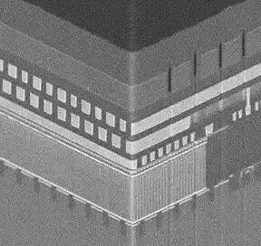
Panoramic view of OCTRAM (Source: KIOXIA, same below)

Traditional DRAM cells are generally 1T1C, meaning one access transistor plus one capacitor. Its problem is: as the cell continues to shrink, the capacitor becomes harder to make, and transistor leakage also increases refresh power consumption. KIOXIA's OCTRAM attempts to reduce leakage through InGaZnO transistors and push the cell structure towards higher density.
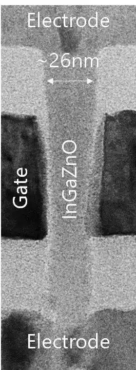
Cross-sectional TEM image of the InGaZnO vertical transistor

Due to its large bandgap and high electron mobility, InGaZnO transistors can theoretically achieve both ultra-low leakage and high on-current. KIOXIA, by optimizing contact electrode materials and spacer thickness, experimentally achieved over 15μA on-current while also realizing ultra-low leakage current below 10⁻¹⁸ A (as shown in the figure below). A significant portion of DRAM power consumption comes from refresh. Lower leakage leads to longer data retention time, reducing refresh pressure. Therefore, the core value of OCTRAM is using low-leakage oxide semiconductor transistors to reduce DRAM refresh power consumption.
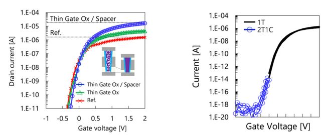
(a) On-current characteristics and (b) Off-current characteristics of the developed InGaZnO transistor

In September 2025, KIOXIA disclosed further reliability research on OCTRAM, focusing on TDDB lifetime issues of sub-25nm Gate-All-Around vertical InGaZnO transistors. TDDB stands for Time-Dependent Dielectric Breakdown. Simply put, it's whether the transistor's insulating layer gradually degrades and eventually fails under long-term electric field stress. KIOXIA stated they found lifetime degradation stems from two factors: intrinsic factors from scaling and extrinsic factors from the manufacturing process. By optimizing the process and reducing extrinsic degradation, KIOXIA achieved a projected TDDB lifetime exceeding 10 years.

In December 2025, KIOXIA announced progress closer to the core of 3D DRAM: developing oxide-semiconductor channel transistors capable of high stacking, having fabricated 8-layer horizontal transistor stacks with on-current exceeding 30μA and off-current below 1 aA, i.e., 10⁻¹⁸ A.

As of now, KIOXIA's 3D DRAM remains in the forefront R&D stage, not yet a commercial product.

KIOXIA is not a traditional DRAM giant, but its accumulated expertise in stacking processes, material integration, and array manufacturing from 3D NAND may give it an entry point in exploring next-generation 3D DRAM. Semiconductor Engineering also analyzed that KIOXIA's 3D DRAM path leverages mature oxide/nitride stacking capabilities from NAND to achieve lower-cost bit scaling, then uses IGZO to replace the channel to reduce thermal degradation issues.

However, one crucial point to emphasize is: KIOXIA's 3D DRAM is not HBM. HBM is packaging-level 3D; it stacks already manufactured DRAM dies to address high-bandwidth needs next to GPUs. KIOXIA's 3D DRAM is device/cell-level 3D; it aims to solve the problem of scaling the DRAM cell itself. Therefore, KIOXIA is not directly chasing HBM but is exploring a more fundamental 3D DRAM device path. If this path matures in the future, it may open a new technology branch for high-capacity, low-power working memory in the AI era.

Although 3D DRAM is still far from true commercialization. It currently resembles more of a future-facing technology ticket than an immediate revenue-contributing product line. But for KIOXIA, the significance of this ticket is not small. In the short term, KIOXIA can capitalize on the NAND recovery driven by AI; in the medium term, it advances high-layer BiCS FLASH; and in the long term, it bets on 3D DRAM, extending its 3D stacking capabilities from NAND to DRAM.

Conclusion

From massive losses and merger deadlock to the super myth of surpassing Toyota to become Japan's top-valued company in 2026, KIOXIA's rollercoaster trajectory is almost filled with the brutality and allure of the semiconductor memory industry. It was once cold-shouldered by capital markets for its single product line and missing the HBM wave, yet amid the tsunami of 'massive data flow' triggered by AI large models, it ushered in its own golden era by steadfastly adhering to NAND flash memory.

KIOXIA's comeback may not yet prove that Japanese semiconductors have truly revived. But at least it demonstrates one thing: in the semiconductor industry, a low point does not necessarily lead to exit. As long as technological assets remain, the realignment of cycles, capital, and demand can at any time bring a forgotten company back to the center of the table.

For KIOXIA, finding a long-term balance between fervent capital追捧 (pursuit) and the冷酷 (harsh) industry cycles moving forward will determine whether this lone sprout carrying the hopes of Japanese semiconductor revival is merely a fleeting flower in the AI supercycle or truly opens a new storage empire of its own.

*Disclaimer: This article was originally written by the author. The content represents the author's personal views. Semiconductor Industry Insights republishes it to convey a different perspective. This does not imply Semiconductor Industry Insights' agreement with or support for this view. If you have any objections, please contact Semiconductor Industry Insights.

Cryptos en tendance

Questions liées

QWhat triggered Kioxia's dramatic turnaround from a loss-making 'hot potato' to a stock market sensation in Japan?

AKioxia's dramatic turnaround was primarily triggered by the explosive demand for AI storage. The advent of large-scale AI models fundamentally shifted the market logic for memory. NAND flash, Kioxia's core product, became a scarce resource for AI inference, model storage, data lakes, enterprise SSDs, and nearline storage, leading to a supply shortage and surging profitability.

QWhat are the two key technologies (acronyms) introduced in Kioxia's 8th generation BiCS FLASH that significantly improved performance?

AThe two key technologies introduced in Kioxia's 8th generation BiCS FLASH are CBA (CMOS directly Bonded to Array) and OPS (On Pitch Select Gate). CBA improves density and speed by bonding separately optimized CMOS and array wafers, while OPS increases storage density by eliminating dummy areas within the memory array.

QWhat is the main technical advantage of Kioxia's OCTRAM (3D DRAM) technology over traditional DRAM?

AThe main technical advantage of Kioxia's OCTRAM technology is its use of InGaZnO (Oxide-Semiconductor) transistors, which offer extremely low leakage current (off-state current). This dramatically reduces refresh power consumption, a major challenge for traditional DRAM as it scales down, thereby enabling higher density and lower power 3D DRAM architectures.

QHow does Kioxia's approach to 3D DRAM (OCTRAM) fundamentally differ from High Bandwidth Memory (HBM)?

AKioxia's 3D DRAM (OCTRAM) is a device/cell-level 3D technology that aims to solve the fundamental scaling problems of the DRAM memory cell itself by stacking transistors vertically. In contrast, HBM is a package-level 3D technology that stacks pre-manufactured DRAM dies to achieve high bandwidth, primarily for GPU-adjacent memory. They address different layers of the memory hierarchy and scaling challenges.

QWhich major investors reaped enormous returns from Kioxia's stock surge, and what was the scale of one of their profits?

AThe major investors were Bain Capital (the parent company) and SK Hynix (an indirect major shareholder). Bain Capital's investment from the 2018 Toshiba Memory buyout became one of the most profitable private equity deals ever, with profits exceeding $15 billion and a return of nearly 20 times. The SK Hynix-led consortium is also expected to realize total profits far exceeding $70 billion.

Lectures associées

Trading

Spot

Articles tendance

Qu'est ce que $S$

Comprendre SPERO : Un aperçu complet Introduction à SPERO Alors que le paysage de l'innovation continue d'évoluer, l'émergence des technologies web3 et des projets de cryptomonnaie joue un rôle central dans la façon dont se dessine l'avenir numérique. Un projet qui a attiré l'attention dans ce domaine dynamique est SPERO, désigné comme SPERO,$$s$. Cet article vise à rassembler et à présenter des informations détaillées sur SPERO, afin d'aider les passionnés et les investisseurs à comprendre ses fondations, ses objectifs et ses innovations dans les domaines du web3 et de la crypto. Qu'est-ce que SPERO,$$s$ ? SPERO,$$s$ est un projet unique dans l'espace crypto qui cherche à tirer parti des principes de décentralisation et de la technologie blockchain pour créer un écosystème qui favorise l'engagement, l'utilité et l'inclusion financière. Le projet est conçu pour faciliter les interactions entre pairs de nouvelles manières, offrant aux utilisateurs des solutions et des services financiers innovants. Au cœur de SPERO,$$s$, l'objectif est d'autonomiser les individus en fournissant des outils et des plateformes qui améliorent l'expérience utilisateur dans l'espace des cryptomonnaies. Cela inclut la possibilité de méthodes de transaction plus flexibles, la promotion d'initiatives dirigées par la communauté et la création de voies pour des opportunités financières via des applications décentralisées (dApps). La vision sous-jacente de SPERO,$$s$ tourne autour de l'inclusivité, visant à combler les lacunes au sein de la finance traditionnelle tout en exploitant les avantages de la technologie blockchain. Qui est le créateur de SPERO,$$s$ ? L'identité du créateur de SPERO,$$s$ reste quelque peu obscure, car il existe peu de ressources publiques fournissant des informations détaillées sur son ou ses fondateurs. Ce manque de transparence peut découler de l'engagement du projet envers la décentralisation—une éthique que de nombreux projets web3 partagent, privilégiant les contributions collectives plutôt que la reconnaissance individuelle. En centrant les discussions autour de la communauté et de ses objectifs collectifs, SPERO,$$s$ incarne l'essence de l'autonomisation sans désigner des individus spécifiques. Ainsi, comprendre l'éthique et la mission de SPERO reste plus important que d'identifier un créateur unique. Qui sont les investisseurs de SPERO,$$s$ ? SPERO,$$s$ est soutenu par une diversité d'investisseurs allant des capital-risqueurs aux investisseurs providentiels dédiés à favoriser l'innovation dans le secteur crypto. L'objectif de ces investisseurs s'aligne généralement avec la mission de SPERO—priorisant les projets qui promettent des avancées technologiques sociétales, l'inclusivité financière et la gouvernance décentralisée. Ces fondations d'investisseurs s'intéressent généralement à des projets qui non seulement offrent des produits innovants, mais qui contribuent également positivement à la communauté blockchain et à ses écosystèmes. Le soutien de ces investisseurs renforce SPERO,$$s$ en tant que concurrent notable dans le domaine en rapide évolution des projets crypto. Comment fonctionne SPERO,$$s$ ? SPERO,$$s$ utilise un cadre multifacette qui le distingue des projets de cryptomonnaie conventionnels. Voici quelques-unes des caractéristiques clés qui soulignent son unicité et son innovation : Gouvernance décentralisée : SPERO,$$s$ intègre des modèles de gouvernance décentralisée, permettant aux utilisateurs de participer activement aux processus de décision concernant l'avenir du projet. Cette approche favorise un sentiment de propriété et de responsabilité parmi les membres de la communauté. Utilité du token : SPERO,$$s$ utilise son propre token de cryptomonnaie, conçu pour servir diverses fonctions au sein de l'écosystème. Ces tokens permettent des transactions, des récompenses et la facilitation des services offerts sur la plateforme, améliorant ainsi l'engagement et l'utilité globaux. Architecture en couches : L'architecture technique de SPERO,$$s$ supporte la modularité et l'évolutivité, permettant une intégration fluide de fonctionnalités et d'applications supplémentaires à mesure que le projet évolue. Cette adaptabilité est primordiale pour maintenir la pertinence dans le paysage crypto en constante évolution. Engagement communautaire : Le projet met l'accent sur des initiatives dirigées par la communauté, utilisant des mécanismes qui incitent à la collaboration et aux retours d'expérience. En cultivant une communauté forte, SPERO,$$s$ peut mieux répondre aux besoins des utilisateurs et s'adapter aux tendances du marché. Accent sur l'inclusion : En proposant des frais de transaction bas et des interfaces conviviales, SPERO,$$s$ vise à attirer une base d'utilisateurs diversifiée, y compris des individus qui n'ont peut-être pas engagé auparavant dans l'espace crypto. Cet engagement envers l'inclusion s'aligne avec sa mission globale d'autonomisation par l'accessibilité. Chronologie de SPERO,$$s$ Comprendre l'histoire d'un projet fournit des aperçus cruciaux sur sa trajectoire de développement et ses jalons. Voici une chronologie suggérée cartographiant les événements significatifs dans l'évolution de SPERO,$$s$ : Phase de conceptualisation et d'idéation : Les idées initiales formant la base de SPERO,$$s$ ont été conçues, s'alignant étroitement avec les principes de décentralisation et de concentration sur la communauté au sein de l'industrie blockchain. Lancement du livre blanc du projet : Suite à la phase conceptuelle, un livre blanc complet détaillant la vision, les objectifs et l'infrastructure technologique de SPERO,$$s$ a été publié pour susciter l'intérêt et les retours de la communauté. Construction de la communauté et engagements précoces : Des efforts de sensibilisation actifs ont été entrepris pour construire une communauté d'adopteurs précoces et d'investisseurs potentiels, facilitant les discussions autour des objectifs du projet et recueillant du soutien. Événement de génération de tokens : SPERO,$$s$ a organisé un événement de génération de tokens (TGE) pour distribuer ses tokens natifs aux premiers soutiens et établir une liquidité initiale au sein de l'écosystème. Lancement de la première dApp : La première application décentralisée (dApp) associée à SPERO,$$s$ a été mise en ligne, permettant aux utilisateurs d'interagir avec les fonctionnalités principales de la plateforme. Développement continu et partenariats : Des mises à jour et des améliorations continues des offres du projet, y compris des partenariats stratégiques avec d'autres acteurs de l'espace blockchain, ont façonné SPERO,$$s$ en un acteur compétitif et évolutif sur le marché crypto. Conclusion SPERO,$$s$ se dresse comme un témoignage du potentiel du web3 et de la cryptomonnaie pour révolutionner les systèmes financiers et autonomiser les individus. Avec un engagement envers la gouvernance décentralisée, l'engagement communautaire et des fonctionnalités conçues de manière innovante, il ouvre la voie vers un paysage financier plus inclusif. Comme pour tout investissement dans l'espace crypto en rapide évolution, les investisseurs et utilisateurs potentiels sont encouragés à mener des recherches approfondies et à s'engager de manière réfléchie avec les développements en cours au sein de SPERO,$$s$. Le projet illustre l'esprit d'innovation de l'industrie crypto, invitant à une exploration plus approfondie de ses nombreuses possibilités. Bien que le parcours de SPERO,$$s$ soit encore en cours, ses principes fondamentaux pourraient en effet influencer l'avenir de nos interactions avec la technologie, la finance et entre nous dans des écosystèmes numériques interconnectés.

131 vues totalesPublié le 2024.12.17Mis à jour le 2024.12.17

Qu'est ce que $S$

Qu'est ce que AGENT S

Agent S : L'avenir de l'interaction autonome dans Web3 Introduction Dans le paysage en constante évolution de Web3 et des cryptomonnaies, les innovations redéfinissent constamment la manière dont les individus interagissent avec les plateformes numériques. Un projet pionnier, Agent S, promet de révolutionner l'interaction homme-machine grâce à son cadre agentique ouvert. En ouvrant la voie à des interactions autonomes, Agent S vise à simplifier des tâches complexes, offrant des applications transformantes dans l'intelligence artificielle (IA). Cette exploration détaillée plongera dans les subtilités du projet, ses caractéristiques uniques et les implications pour le domaine des cryptomonnaies. Qu'est-ce qu'Agent S ? Agent S se présente comme un cadre agentique ouvert révolutionnaire, spécifiquement conçu pour relever trois défis fondamentaux dans l'automatisation des tâches informatiques : Acquisition de connaissances spécifiques au domaine : Le cadre apprend intelligemment à partir de diverses sources de connaissances externes et d'expériences internes. Cette approche double lui permet de construire un riche répertoire de connaissances spécifiques au domaine, améliorant ainsi sa performance dans l'exécution des tâches. Planification sur de longs horizons de tâches : Agent S utilise une planification hiérarchique augmentée par l'expérience, une approche stratégique qui facilite la décomposition et l'exécution efficaces de tâches complexes. Cette fonctionnalité améliore considérablement sa capacité à gérer plusieurs sous-tâches de manière efficace et efficiente. Gestion d'interfaces dynamiques et non uniformes : Le projet introduit l'Interface Agent-Ordinateur (ACI), une solution innovante qui améliore l'interaction entre les agents et les utilisateurs. En utilisant des Modèles de Langage Multimodaux de Grande Taille (MLLMs), Agent S peut naviguer et manipuler sans effort diverses interfaces graphiques. Grâce à ces fonctionnalités pionnières, Agent S fournit un cadre robuste qui aborde les complexités impliquées dans l'automatisation de l'interaction humaine avec les machines, préparant le terrain pour d'innombrables applications en IA et au-delà. Qui est le créateur d'Agent S ? Bien que le concept d'Agent S soit fondamentalement innovant, des informations spécifiques sur son créateur restent insaisissables. Le créateur est actuellement inconnu, ce qui souligne soit le stade naissant du projet, soit le choix stratégique de garder les membres fondateurs sous le radar. Quoi qu'il en soit, l'accent reste mis sur les capacités et le potentiel du cadre. Qui sont les investisseurs d'Agent S ? Étant donné qu'Agent S est relativement nouveau dans l'écosystème cryptographique, des informations détaillées concernant ses investisseurs et soutiens financiers ne sont pas explicitement documentées. Le manque d'aperçus publiquement disponibles sur les fondations d'investissement ou les organisations soutenant le projet soulève des questions sur sa structure de financement et sa feuille de route de développement. Comprendre le soutien est crucial pour évaluer la durabilité du projet et son impact potentiel sur le marché. Comment fonctionne Agent S ? Au cœur d'Agent S se trouve une technologie de pointe qui lui permet de fonctionner efficacement dans divers environnements. Son modèle opérationnel est construit autour de plusieurs caractéristiques clés : Interaction homme-ordinateur semblable à l'humain : Le cadre offre une planification IA avancée, s'efforçant de rendre les interactions avec les ordinateurs plus intuitives. En imitant le comportement humain dans l'exécution des tâches, il promet d'élever l'expérience utilisateur. Mémoire narrative : Utilisée pour tirer parti des expériences de haut niveau, Agent S utilise la mémoire narrative pour suivre les historiques de tâches, améliorant ainsi ses processus de prise de décision. Mémoire épisodique : Cette fonctionnalité fournit aux utilisateurs un accompagnement étape par étape, permettant au cadre d'offrir un soutien contextuel au fur et à mesure que les tâches se déroulent. Support pour OpenACI : Avec la capacité de fonctionner localement, Agent S permet aux utilisateurs de garder le contrôle sur leurs interactions et flux de travail, s'alignant avec l'éthique décentralisée de Web3. Intégration facile avec des API externes : Sa polyvalence et sa compatibilité avec diverses plateformes IA garantissent qu'Agent S peut s'intégrer sans effort dans des écosystèmes technologiques existants, en faisant un choix attrayant pour les développeurs et les organisations. Ces fonctionnalités contribuent collectivement à la position unique d'Agent S dans l'espace crypto, alors qu'il automatise des tâches complexes en plusieurs étapes avec un minimum d'intervention humaine. À mesure que le projet évolue, ses applications potentielles dans Web3 pourraient redéfinir la manière dont les interactions numériques se déroulent. Chronologie d'Agent S Le développement et les jalons d'Agent S peuvent être encapsulés dans une chronologie qui met en évidence ses événements significatifs : 27 septembre 2024 : Le concept d'Agent S a été lancé dans un document de recherche complet intitulé “Un cadre agentique ouvert qui utilise les ordinateurs comme un humain”, présentant les bases du projet. 10 octobre 2024 : Le document de recherche a été rendu publiquement disponible sur arXiv, offrant une exploration approfondie du cadre et de son évaluation de performance basée sur le benchmark OSWorld. 12 octobre 2024 : Une présentation vidéo a été publiée, fournissant un aperçu visuel des capacités et des caractéristiques d'Agent S, engageant davantage les utilisateurs et investisseurs potentiels. Ces jalons dans la chronologie illustrent non seulement les progrès d'Agent S, mais indiquent également son engagement envers la transparence et l'engagement communautaire. Points clés sur Agent S Alors que le cadre Agent S continue d'évoluer, plusieurs attributs clés se distinguent, soulignant sa nature innovante et son potentiel : Cadre innovant : Conçu pour offrir une utilisation intuitive des ordinateurs semblable à l'interaction humaine, Agent S propose une approche nouvelle de l'automatisation des tâches. Interaction autonome : La capacité d'interagir de manière autonome avec les ordinateurs via une interface graphique signifie un bond vers des solutions informatiques plus intelligentes et efficaces. Automatisation des tâches complexes : Avec sa méthodologie robuste, il peut automatiser des tâches complexes en plusieurs étapes, rendant les processus plus rapides et moins sujets aux erreurs. Amélioration continue : Les mécanismes d'apprentissage permettent à Agent S de s'améliorer grâce à ses expériences passées, améliorant continuellement sa performance et son efficacité. Polyvalence : Son adaptabilité à travers différents environnements d'exploitation comme OSWorld et WindowsAgentArena garantit qu'il peut servir un large éventail d'applications. Alors qu'Agent S se positionne dans le paysage Web3 et crypto, son potentiel à améliorer les capacités d'interaction et à automatiser les processus représente une avancée significative dans les technologies IA. Grâce à son cadre innovant, Agent S incarne l'avenir des interactions numériques, promettant une expérience plus fluide et efficace pour les utilisateurs à travers divers secteurs. Conclusion Agent S représente un saut audacieux en avant dans le mariage de l'IA et de Web3, avec la capacité de redéfinir notre interaction avec la technologie. Bien qu'il soit encore à ses débuts, les possibilités de son application sont vastes et convaincantes. Grâce à son cadre complet abordant des défis critiques, Agent S vise à mettre les interactions autonomes au premier plan de l'expérience numérique. À mesure que nous plongeons plus profondément dans les domaines des cryptomonnaies et de la décentralisation, des projets comme Agent S joueront sans aucun doute un rôle crucial dans la façon dont la technologie et la collaboration homme-machine évolueront à l'avenir.

893 vues totalesPublié le 2025.01.14Mis à jour le 2025.01.14

Qu'est ce que AGENT S

Comment acheter S

Bienvenue sur HTX.com ! Nous vous permettons d'acheter Sonic (S) de manière simple et pratique. Suivez notre guide étape par étape pour commencer votre parcours crypto.Étape 1 : Création de votre compte HTXUtilisez votre adresse e-mail ou votre numéro de téléphone pour ouvrir un compte sur HTX gratuitement. L'inscription se fait en toute simplicité et débloque toutes les fonctionnalités.Créer mon compteÉtape 2 : Choix du mode de paiement (rubrique Acheter des cryptosCarte de crédit/débit : utilisez votre carte Visa ou Mastercard pour acheter instantanément Sonic (S).Solde :utilisez les fonds du solde de votre compte HTX pour trader en toute simplicité.Prestataire tiers :pour accroître la commodité d'utilisation, nous avons ajouté des modes de paiement populaires tels que Google Pay et Apple Pay.P2P :tradez directement avec d'autres utilisateurs sur HTX.OTC (de gré à gré) : nous offrons des services personnalisés et des taux de change compétitifs aux traders.Étape 3 : stockage de vos Sonic (S)Après avoir acheté vos Sonic (S), stockez-les sur votre compte HTX. Vous pouvez également les envoyer ailleurs via un transfert sur la blockchain ou les utiliser pour trader d'autres cryptos.Étape 4 : tradez des Sonic (S)Tradez facilement Sonic (S) sur le marché Spot de HTX. Il vous suffit d'accéder à votre compte, de sélectionner la paire de trading, d'exécuter vos trades et de les suivre en temps réel. Nous offrons une expérience conviviale aux débutants comme aux traders chevronnés.

1.9k vues totalesPublié le 2025.01.15Mis à jour le 2026.06.02

Comment acheter S

Discussions

Bienvenue dans la Communauté HTX. Ici, vous pouvez vous tenir informé(e) des derniers développements de la plateforme et accéder à des analyses de marché professionnelles. Les opinions des utilisateurs sur le prix de S (S) sont présentées ci-dessous.

活动图片