For South Koreans, the hardest thing to accept is probably losing.
On June 28th, after the South Korean national football team was eliminated from the World Cup group stage, President Lee Jae-myung criticized the team on social media for "betraying the nation's expectations" and demanded a thorough investigation by the Korea Football Association into the reasons for the failure.
The next day, President Lee Jae-myung had composed himself and stood side-by-side with Samsung Electronics Chairman Lee Jae-yong and SK Group Chairman Chey Tae-won on a press conference stage, bowing 90 degrees to thank them for their massive investment plans.
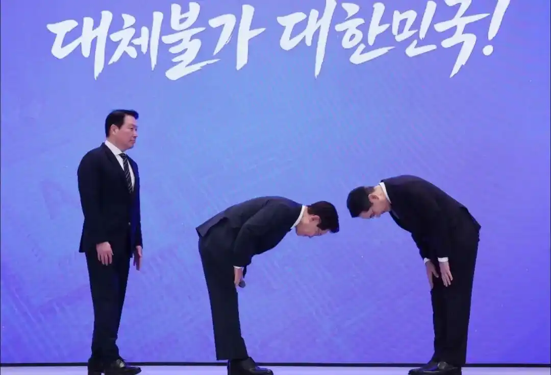
The scene of the "Three Super Projects" briefing session. Source | Internet
At this press conference, the South Korean government, together with the two corporations, unveiled a sky-high investment plan equivalent to 2.33 times South Korea's GDP. The South Korean government's investment in this plan totals 1,461 trillion won (approximately 6.4 trillion yuan RMB), with the majority poured into semiconductor production, of which the semiconductor production base in the southwest region alone accounts for 800 trillion won.
But if you are familiar with the history of the semiconductor industry, you will notice something unusual.
For the past three decades, the South Korean semiconductor industry has been adept at "counter-cyclical investment." During industry downturns, South Korean semiconductor companies would instead increase capital expenditure, expand production capacity, and seize market share using their low-cost advantage.
When the cycle recovered, the new capacity would be released just in time, allowing them to reap super profits by raising prices and maintaining volume.
In recent years, the growth in AI computing demand has ushered memory chips into a super boom cycle, with prices rising continuously; following the previous script, the giants should have started to "throttle" supply, slowly releasing capacity to maintain high profits for as long as possible.
But why is South Korea making such a massive, aggressive investment push during an industry upcycle this time? What are they worried about? Looking back along the forty-year history of East Asian competition in the semiconductor industry, the answer is not hard to find.
01 The "History of Competition" in Semiconductors: Japan vs. South Korea
The semiconductor business has been a money-burning game from day one. A single wafer fab costs tens of billions to start, with factories, equipment, and tape-outs—each step is a money pit.
Without the backing of a nation's strength, newcomers couldn't even get a seat at the table.
In East Asia, Japan was the first to master the model of "state-led system + industrial capital."
In the early 1970s, IBM announced the development of its "Future System" using Very Large Scale Integration (VLSI), pulling ahead of Japan technologically. Simultaneously, the US government pressured Japan to open its computer and semiconductor markets, an event that could be called the "Black Ships of Semiconductors."
Cornered, Japan quickly came up with a countermeasure.
In 1976, Japan's Ministry of International Trade and Industry (MITI) adopted the "state-led system + industrial capital" model, uniting five major companies—Hitachi, NEC, Fujitsu, Mitsubishi, and Toshiba—to raise 72 billion yen (approximately 236 million USD) and establish the "VLSI Technology Research Association."
The goal was pure: catch up with the US.
The effect was immediate.
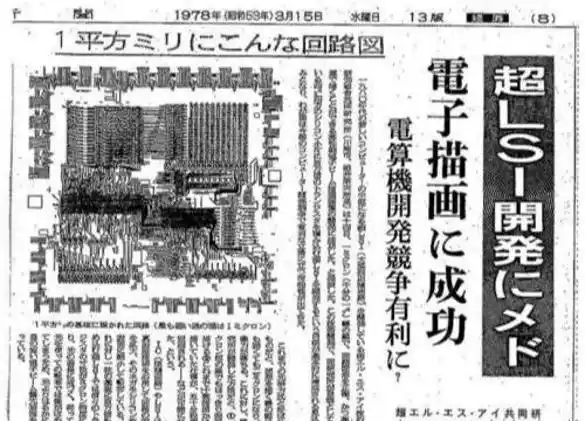
A 1978 Japanese newspaper report on the breakthrough in VLSI. Source | Internet
By the end of 1982, Japan's 64K DRAM accounted for 66% of the international market. By the late 1980s, Japan had captured 80% of the global DRAM market, beating back American manufacturers like Intel.
At that time, South Korea was simply not in Japan's competitive field of vision.
But just as Japanese semiconductors were at their peak, a South Korean man announced in Tokyo that he was entering the semiconductor business.
He said: "I want to advance the semiconductor business based on our nation's unique tenacious spirit and creativity."
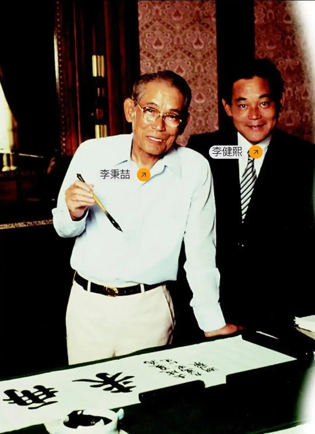
Samsung Group founder Lee Byung-chul with his third son, Lee Kun-hee. Source | Internet
This old man was Samsung founder Lee Byung-chul, and these words later became known as the "Tokyo Declaration."
But in Tokyo at that time, on the Japanese home turf where they were most triumphant, no one took these words seriously.
Intel of the US even mocked him as a "delusional exaggerator," while the CEO of Japan's Mitsubishi publicly declared: the semiconductor industry simply isn't suitable for South Korea.
At that time, Samsung could barely produce low-end integrated circuits for home appliances and didn't even have a proper DRAM production line.
But this ridiculed "delusion" would, in less than ten years, make the entire Japanese DRAM industry tremble with fear.
Back then, the global chip industry was firmly controlled by American companies like Micron and Japanese giants like Mitsubishi and Sharp. The US and Japanese companies kept the technological gates tightly shut. To gain entry-level technology, Samsung dispatched batch after batch of researchers to companies like Micron and Sharp.
The process was humiliating.
Micron had verbally agreed to provide relatively outdated design drawings for $4 million, but later reneged using the excuse of "reading literature without permission" and kicked Samsung personnel out of the company.
As for Sharp, while they ostensibly agreed to Samsung's request, they kept a tight watch, even forbidding Samsung personnel from approaching the latest production lines.
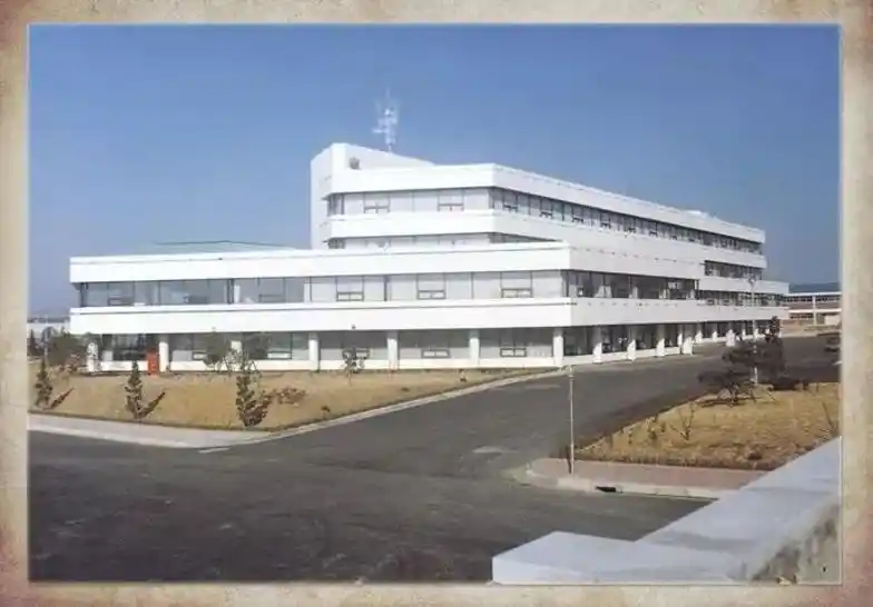
Samsung's Suwon R&D Center built in 1979. Source | Internet
Samsung researchers couldn't even get basic data like the factory's floor area. One researcher used the spacing of his fingers, his height, and his step count to roughly record the factory's approximate area and other parameters.
For example, he measured the production line width as 30 steps and length as 222 steps.
However, as an insider who had worked at Samsung Semiconductor for many years later recalled: "This data was obviously insufficient for building a high-tech factory."
No one expected that this ridiculed "delusion" would, in less than ten years, make the entire Japanese DRAM industry tremble with fear.
And the turning point of victory and defeat lay hidden in the shift of industrial logic.
Japanese DRAM manufacturers' pursuit of extreme quality stemmed from the era when their main customers were banks, railways, and telephone and telegraph companies.
These customers had one requirement for DRAM: it absolutely must not fail.
Relying on this extreme quality, Japan defeated the US in the 1980s, capturing 80% of the global DRAM market.
But Japan's turning point also began at this time.
The 1985 Plaza Accord caused the Japanese yen to appreciate sharply, severely weakening the export competitiveness of Japanese products.
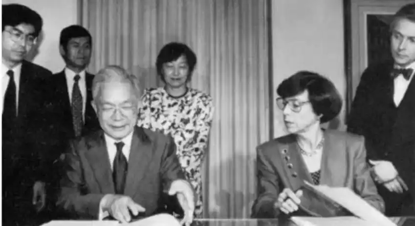
The signing of the US-Japan Semiconductor Agreement. Source | Internet
In 1986, the US initiated anti-dumping lawsuits against Japanese semiconductor companies, leading to an export restriction agreement between the two sides—Japan's hands were tied, and the expansion capacity of its semiconductor industry was severely constrained.
The external market was also changing. Entering the 1990s, personal computers replaced mainframes as the mainstream.
PCs were consumer electronics; they didn't need 25-year zero-failure "aerospace-grade" quality. Five years of usable life was enough. Cheap, high volume, and fast iteration were key.
The "craftsman spirit" that chased quality became a stumbling block in the industry's pursuit of scale.
The Koreans saw this opportunity and also began using the "state-led system + industrial capital" model to counter-attack the Japanese memory industry.
In 1983, the South Korean government began implementing the "VLSI Technology Joint Development Plan," led by the Korea Institute of Electronic Technology, with participation from major corporations like Samsung, Hyundai, LG, six universities, and an investment of $110 million over three years, with the government covering 57%.
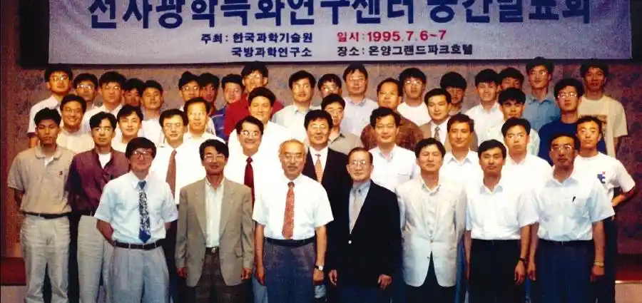
Group photo of personnel at the Korea Electro-Optics Center, an institution aimed at developing thermal imaging, fiber optic, and laser technology. Source | Internet
In 1992, Samsung was the first to launch the world's first 64M DRAM, surpassing Japan's NEC to become the world's largest DRAM manufacturer. In 1993, Samsung's production efficiency surpassed Japan's, officially topping the global DRAM market.
Now it was Japan's turn to panic.
In 1999, to counter Samsung's strong rise, the Japanese government led the integration of the DRAM businesses of Hitachi, NEC, and Mitsubishi Electric to form Elpida.
After its establishment, Elpida developed rapidly for a time, becoming the world's third-largest DRAM manufacturer. Even during the 2009 financial crisis, the Japanese government injected 30 billion yen and provided 100 billion yen in financing guarantees through an amendment to the Industrial Revitalization Law.
The speed of government bailouts couldn't keep up with the bloodletting of the memory price war. In desperation, Elpida President Yukio Sakamoto made an all-or-nothing decision: a 1.6 trillion yen capacity expansion plan, attempting one final gamble for a sliver of survival.
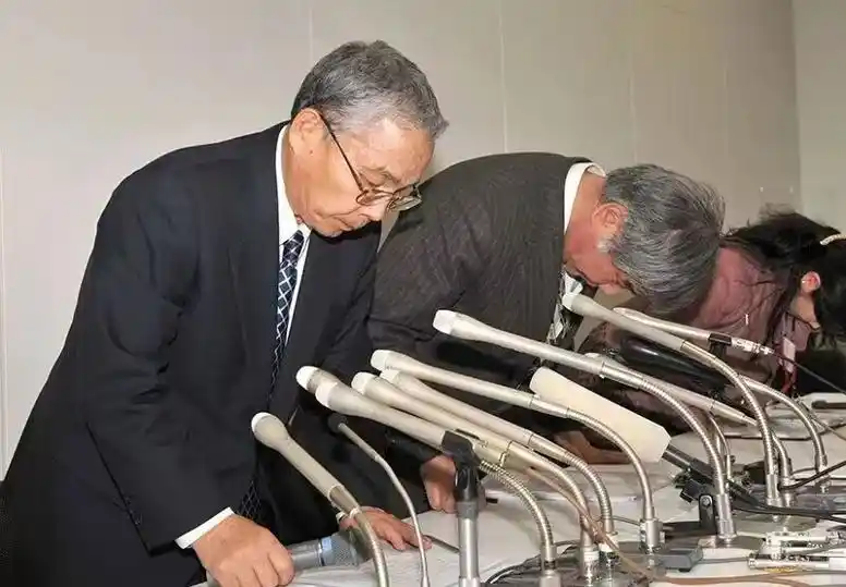
Elpida President Yukio Sakamoto at the bankruptcy press conference. Source | Internet
It is rumored that when the Elpida president sought help, some Japanese official agency coldly responded: "Japan doesn't need memory. We can just buy it from South Korea."
In February 2012, Elpida, with debts reaching 448 billion yen (approximately $5.5 billion), applied for bankruptcy protection. In July of the same year, it was acquired by Micron Technology, one of today's memory triumvirate, for about $2.5 billion.
Thus, the memory industry formed the current tripartite structure of "Samsung, SK Hynix, and Micron."
Looking back at this history, the essence of victory and defeat was a competition in the efficiency of two "state-led system + industrial capital" models.
Japan used this model to catch up with the US, reaching the top in the 1980s; South Korea used the same model to counter and defeat Japan, replacing it in the 1990s.
Every time the throne changes hands, it's a latercomer using more determined investment and more ruthless endurance to outlast the predecessor.
02 China's Two Memory Horses: Yangtze Memory and ChangXin Memory
By 2016, the iron curtain of the global memory market had remained in place for over a decade.
Samsung, SK Hynix, and Micron controlled over 95% of the high-end market. Patent walls, capital barriers, and process generation gaps were like three layers of iron walls—latercomers couldn't even touch the table.
But that year, the cities of Wuhan and Hefei almost simultaneously pressed the start button.
Yangtze Memory Technologies (YMTC) in the south and ChangXin Memory Technologies (CXMT) in the north—one attacking NAND flash, the other breaking into DRAM—like two fire-hardened awls, tried to chisel a gap into the airtight oligopoly.
But none of their starting paths were smooth.
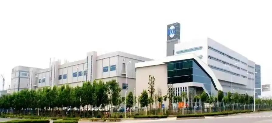
XMC (Wuhan Xinxin Semiconductor Manufacturing Corp.) integrated circuit factory building in Wuhan. Source | Internet
The starting point for Yangtze Memory was XMC (Wuhan Xinxin), a "veteran unit" that had endured losses for ten years.
In 2006, promoted by SMIC founder Richard Chang, XMC was formally established.
The provincial, municipal, and Donghu High-Tech Zone governments jointly invested, building central China's first 12-inch integrated circuit production line on a patch of wasteland, giving birth to a spark of independent intellectual property.
But when ideals collided with reality, they shattered silently.
From 2006 to 2017, XMC was in the red for eleven consecutive years, never finding the right market direction. What truly changed the company's fate was the arrival of Simon Yang.
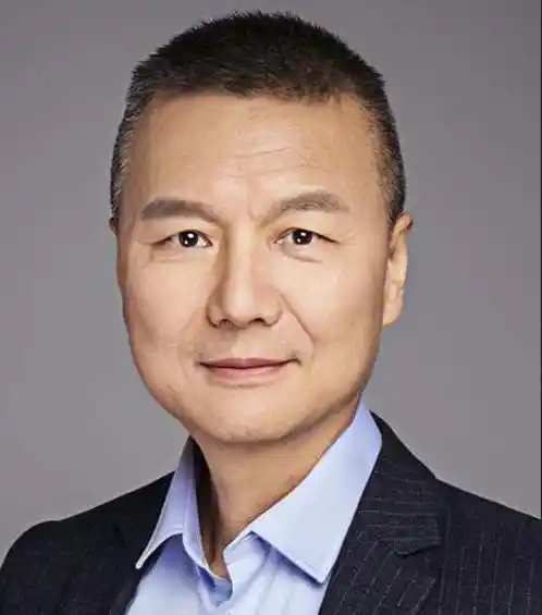
Simon Yang, CEO of Yangtze Memory Technologies Co., Ltd. Source | Internet
Simon Yang's resume is top-tier in China's semiconductor industry. He worked at Intel for over ten years and served as Chief Operating Officer of SMIC in 2010.
In 2013, Simon Yang became the CEO of XMC. Previously, XMC had long relied on external management for operations, and its independent system was not yet mature. Upon taking office, Simon Yang built a complete R&D, operations, and market management structure, cultivated a local professional team, and established a direction of independent R&D.
In July 2016, Yangtze Memory Technologies (YMTC) was officially established, with XMC being wholly integrated as a subsidiary.
YMTC's leadership team gathered a group of capable individuals from China's semiconductor industry:
Zhao Weiguo (then Chairman of Tsinghua Unigroup) served as Chairman;
Ding Wenwu (then General Manager of the National Integrated Circuit Industry Investment Fund) served as Vice Chairman;
Simon Yang (former COO of SMIC) served as General Manager;
Charles Kao (then Global Executive Vice President of Tsinghua Unigroup, known as the "Memory Godfather of Taiwan") joined as an Executive Director.
These four brought together Tsinghua Unigroup's industrial capital, the National Big Fund's strategic resources, XMC's production line, and the experience of Taiwan's memory industry.
The people were assembled, but which path to take? YMTC's choice was to get on board first.
In 2017, the team spent $1 billion over two years to successfully design and manufacture China's first 32-layer 3D NAND flash chip. Although 32 layers were far behind the then-mainstream 64-layer and 96-layer products, at least they had something.
The competitors' reaction was quite relaxed. Samsung unhurriedly launched its 64-layer product. Just as YMTC was starting, its opponents had already run another lap.
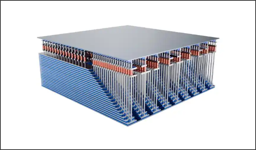
Schematic diagram of the Xtacking technology. Source | Internet
The turning point came in 2019. That year, based on its self-developed Xtacking architecture, YMTC launched its second-generation 64-layer 3D NAND flash and officially began mass production.
Unlike traditional 3D NAND flash, which builds the "foundation" (peripheral circuits) and the "building" (memory cells) together, the Xtacking architecture first builds the "foundation" and the "building" on two separate wafers. After both are completed, a special "bonding" technology is used to precisely bond the two wafers together.
This path was untrodden by others. Chief Scientist Huo Zongliang later said: "Xtacking is our unique path, truly carving out a new flash memory path belonging to China." The advantage of this path is that it can shorten product development time by three months and production cycles by 20%.
But fate seemed to always work against YMTC. In the same year the 64-layer went into mass production, Samsung released its 128-layer flash chip. YMTC's product became "obsolete" as soon as it was launched.
Following the giants' roadmap step-by-step meant always eating dust.
The flexibility and development speed of the Xtacking architecture made YMTC suddenly realize: if peripheral circuits and memory cells can be developed separately and advanced in parallel, why wait?
So they made a riskier decision: skip the next generation of 96-layer after 64-layer and directly develop 128-layer.
In 2020, to ensure R&D progress, YMTC immediately established an "Emergency Status Frontline Command Center," and the chip production lines never stopped during this period.
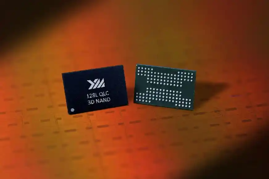
YMTC's X2-6070 128L QLC 1.33Tb 3D NAND. Source | Internet
On April 13 of that year, YMTC announced the successful development of its 128-layer QLC 3D NAND flash.
This was the world's first 128-layer QLC flash. Simon Yang said: "This is the crystallization of the sweat of thousands of R&D personnel." From 32-layer to 128-layer, YMTC took only three years.
It's hard to imagine how many sleepless nights, how many scrapped samples, how many times being left behind and getting back up are hidden behind these layer numbers.
According to Counterpoint data, in Q4 2025, YMTC's global NAND flash share was 11%, ranking sixth globally. In Q3 2025, its share once reached 13%, approaching the fourth position.
If YMTC's story is one of rebirth from desperate straits, then ChangXin Memory's story is one of building a skyscraper on flat ground.
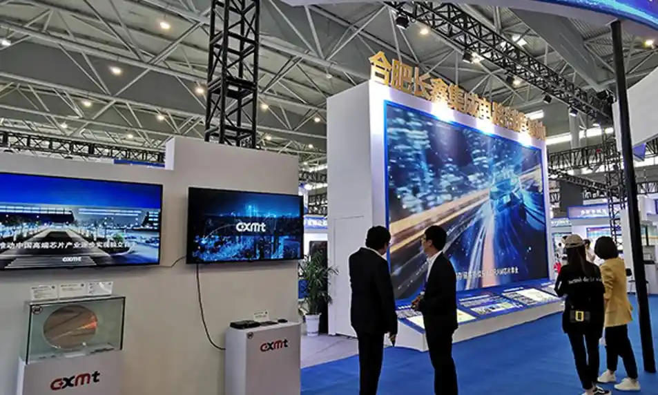
A promotional image for ChangXin Memory Technologies (CXMT). Source | Internet
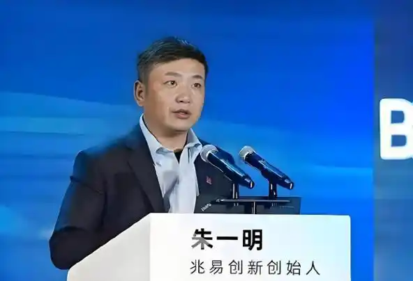
Founder Zhu Yiming graduated from Tsinghua University, went to the US to work on chips, returned to China to found GigaDevice, and reached the top three globally in the NOR flash field. But the NOR Flash market was too small. Zhu Yiming wanted a bigger battlefield. In 2016, he and the city of Hefei came together, deciding to do something even harder: make DRAM.
This project had a code name "506," rumored because on May 6, 2016, the main leaders of Hefei city and the Economic Development Zone, together with Zhu Yiming, discussed Hefei's memory project development strategy.
The barriers to entry for DRAM are higher than for flash. If making flash is "building a building," with relatively relaxed requirements for micro-precision, then making DRAM is like "carving" at the nanometer scale, where each memory cell consists of a precise transistor and an extremely tiny capacitor.
Even more brutal are patents. Samsung, SK Hynix, and Micron have been running in this track for over forty years. The patent walls they've built are high and thick, enough to deter any potential challenger.
It was on such a battlefield where there seemed to be no path that ChangXin found its way.
And the foundation of this path came from a German company that had been bankrupt for ten years—Qimonda.
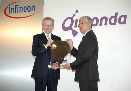
Infineon announces the spin-off of Qimonda; the two CEOs hold up a 12-inch wafer. Source | Internet
In 2006, Qimonda was spun off from Infineon and was then the world's second-largest DRAM supplier, riding high.
But the DRAM track was too brutal. Within three years, it was completely crushed in a price war initiated by Samsung. In January 2009, Qimonda formally declared bankruptcy, becoming a sacrificial lamb to the Koreans' textbook counter-cyclical tactics.
When Qimonda went bankrupt, the technological patents it left behind were not "unique secrets" at that time—they had already been surpassed by a generation or more by Samsung and Hynix. For these three giants, spending billions to buy a pile of technology that lagged behind their own roadmaps, while also taking on the legal risks and integration costs of an acquisition, was a bad deal.
ChangXin, however, took Qimonda out of the bankruptcy vault. Zhu Yiming once said: "Qimonda is not garbage; it's the only admission ticket for China's DRAM."
Through cooperation with Qimonda, ChangXin obtained over ten million technical documents, about 2.8TB of data, including DRAM patent licenses and partial ownership. Founder Zhu Yiming later admitted that these documents formed the foundation of ChangXin's DRAM business.
Most crucially, ChangXin inherited a core technology from Qimonda—BWL (Buried Wordline).
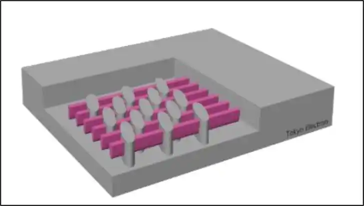
Schematic diagram of the Buried Wordline process. Source | Internet
The idea behind BWL is simple—bury the wordline inside the silicon wafer, wrap it in an insulating layer, completely isolating interference and reducing memory cell failure rates. Based on this technology, ChangXin developed its own 46nm-class BWL cell and further advanced it to the 10nm class.
In terms of technological roadmap, both YMTC and CXMT took risky paths of skipping generations, but YMTC skipped layers, while CXMT skipped nanometers.
After achieving large-scale mass production of 19nm process DDR4 chips in 2019, CXMT didn't methodically refine 18nm. Instead, it directly invested in the R&D of 17nm DDR5, skipping the verified intermediate nodes and betting on the next process generation.
Having a technological spark is one thing; you also need money.
There's a cruel rule in the memory chip industry: it inevitably loses money in the early stages. From 2022 to 2024, ChangXin accumulated losses exceeding 30 billion yuan; by the end of 2025, its cumulative uncovered losses reached 36.65 billion yuan.
An industry saying goes: to start R&D and production of DRAM, you need at least 10 billion yuan in start-up capital per year.
Any private capital would have pulled out long ago.
But Hefei did not pull out.
2019 Global Semiconductor Alliance Summit. Source | Internet
In 2024, a relevant person from Hefei Industry Investment said: "For weak links in the industrial chain like chips, the probability of realizing capital returns in the short term is very small. It must be big capital, long cycles, even spanning several cycles before value investment can ultimately be achieved."
Over ten years of accompanying the run, Hefei state-owned capital accumulated approximately 36.79% equity in ChangXin. This investment delivered a stunning report card in Q1 2026: single-quarter revenue of 50.8 billion yuan and net profit of 24.762 billion yuan.
Returns on the capital side are also close at hand. ChangXin's Science and Technology Innovation Board (STAR Market) IPO has completed registration with the China Securities Regulatory Commission, awaiting only the bell-ringing for listing.
By the end of 2025, ChangXin had captured 7.67% of the global DRAM market share, ranking first in China and fourth globally.
The rise paths of YMTC and CXMT are very similar: introduce and absorb, self-develop, skip generations to catch up, and expand during downturns. Every step was a leap into the unknown. Skipping generations means investing in the next generation before making money from the previous one. Expanding during downturns means continuing to burn money when losses are heaviest.
Especially in 2023, memory chips encountered the "most severe downturn in 13 years," with prices even falling to 0.2 yuan per gigabyte.
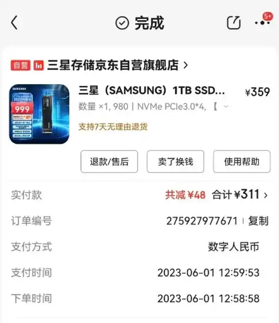
A screenshot from 2023 showing SSD prices. Source | Internet
Netizens posted screenshots of orders from that year, where a Samsung 1TB SSD could be had for just 311 yuan. Even Samsung's own products were selling at this price, indicating how bad the industry was. Samsung, SK Hynix, and Micron couldn't withstand the huge losses and had to cut production to protect prices.
YMTC and CXMT's choice was: you cut production, we expand; you protect prices, we lower them.
Samsung used this exact tactic to outlast its Japanese rivals back in the day. Now, China's "Two Mems" have pulled out the same card. This gamble paid off well—by 2025, the market shares of CXMT and YMTC doubled.
But there's one difference between these two Chinese companies and Samsung back then: extreme discretion.
Samsung had grandly announced its entry into semiconductors in Tokyo, only to be mocked, blocked, and besieged.
CXMT and YMTC seem to have understood this history. Now, you can find many photos of consumer electronics assembly lines online, but if you search for YMTC and CXMT factories, you'll only see building exteriors and office workspaces.
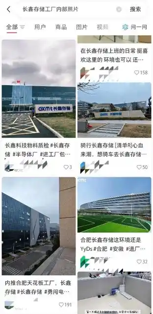
Search results for "ChangXin Memory factory interior photos" on Xiaohongshu (Little Red Book). Source | Internet
As for what the production lines look like, not a single photo can be found.
From obscurity to global fourth and sixth place, China's two memory horses took less than ten years, sending a chill down the spine of South Korea, currently sitting on the memory throne.
03 The Cycle of History: The Chaser Becomes the Incumbent
Returning to the opening question: Why is South Korea making its largest-ever capacity expansion investment during an upcycle?
The answer is evident.
Thirty years ago, South Korea was the chaser making crazy bets during industry downturns, using counter-cyclical investment to outlast its Japanese predecessor. Thirty years later, it has become the incumbent sitting on the throne, while Chinese players below are using almost identical tactics, step by step, to chase it down.
The super-cycle brought by AI is certainly enticing, but what South Korea is truly anxious about is likely the long-term threat behind the cycle.
Past Japan-South Korea competition was essentially an efficiency contest within the same tier. Today's China-South Korea memory industry competition is supported by industrial chains with vastly different levels of completeness.
South Korea has a first-mover technological advantage. China holds the world's largest downstream market for consumer electronics, servers, and computing terminals. From chip design, wafer manufacturing, packaging and testing, to terminal systems, a complete closed loop is forming. Local equipment and materials companies are also breaking through simultaneously, not needing to purchase core equipment and raw materials from abroad everywhere like Samsung did back in the day.
Once the technological generation gap is closed, the scale advantage will quickly tilt.
That's why South Korea is acting contrary to its nature, placing heavy bets ahead of time during a boom cycle, trying to use larger capacity and more advanced processes to widen the gap and keep the chasers firmly behind.
This isn't greed; it's more like fear—fear that the weapon they used to defeat their opponent might one day be used against them.
The most paradoxical thing about history is this: the sword technique you use to slay the dragon will eventually be learned by a latercomer, who will then wield it against you.
But industrial cycles never favor any defender of the status quo.
Thirty years ago, no one believed that resource-poor South Korea could defeat a thriving Japan. Today, similarly, no one can predict what kind of industry landscape the continuously low-key, latent, and counter-trend expanding Chinese memory players will stir up in the future.
This battle to defend the memory throne is far from decided.
Looking back years from now at today's multi-trillion-won investment press conference, people might suddenly realize that this was precisely the prologue to another power shift in East Asia's memory industry.
This article is from the WeChat public account "Phoenix Net Finance," author: Storm Eye