0.7nm Process Chip Emerges, Moore's Law Lives On

marsbitPublished on 2026-06-26Last updated on 2026-06-26

Abstract

IBM has unveiled the world's first sub-1-nanometer (0.7nm) chip technology, integrating nearly 100 billion transistors into an area the size of a fingernail. This breakthrough doubles the transistor density of current 2nm chips and promises a 50% performance gain or a 70% improvement in power efficiency. The achievement is powered by IBM's "NanoStack" architecture, a pioneering 3D design featuring vertically stacked nanosheet transistors. This evolution from FinFET and Gate-All-Around (GAA) technologies offers superior electrostatic control. IBM has demonstrated the technology's viability with functional CMOS inverters and a 40% area reduction in SRAM, crucial for AI chip data bandwidth. Addressing the critical power consumption challenges in AI computing, this advancement extends the roadmap for chip miniaturization. While IBM does not manufacture chips itself, it licenses its process technology to partners. The company projects that NanoStack-based chips could enter production within the next five years, potentially sustaining Moore's Law for another decade.

Is Moore's Law saved?

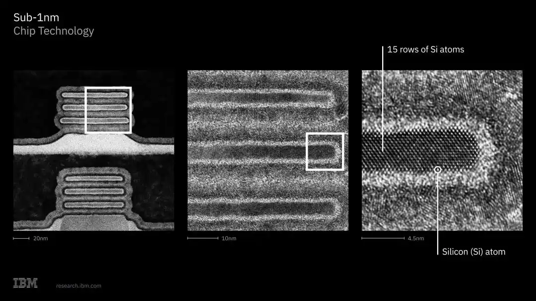
IBM unveiled the world's first 0.7 nanometer chip process node, integrating nearly 100 billion transistors on a chip the size of a fingernail, achieving a density double that of 2nm chips.

Previously, TSMC's most advanced process was 2nm, which had been difficult to advance beyond for years.

NVIDIA CEO Jensen Huang had repeatedly declared Moore's Law dead, but now there is finally a turning point.

0.7 nanometers, or 7 angstroms, marks the first time human-made transistors have broken through the 1 nanometer threshold, approaching the scale of individual atoms (0.1-0.5 nanometers).

Compared to the 2nm process, it can deliver either a 50% performance improvement or a 70% increase in power efficiency; one or the other.

NanoStack Architecture Arrives

The core of this breakthrough is IBM's "NanoStack" architecture, the industry's first 3D vertically stacked transistor design based on nanosheets.

To understand NanoStack, one must first review the path chip architecture has taken in recent years.

In the 7nm and 10nm era, the mainstream solution was FinFET (Fin Field-Effect Transistor) with the gate wrapping around the channel on three sides to control current. Below 5nm, FinFET's leakage issues became increasingly severe and unsustainable.

In 2017, IBM introduced the Gate-All-Around (GAA) nanosheet technology, where the gate completely surrounds the horizontally stacked nanosheet channel on all four sides, significantly enhancing electrostatic control. This became the technical foundation for its 2nm chip and was subsequently adopted by mainstream manufacturers like TSMC and Samsung.

At the end of 2021, IBM and Samsung jointly announced the VTFET (Vertical-Transport Field-Effect Transistor), which changed the current flow direction from horizontal to vertical. Simulation data showed it could either double performance or reduce power consumption by 85% compared to a similarly sized FinFET solution.

This NanoStack is a further extension of the above roadmap.

Its method is:

Take two wafers with nanosheet transistors, invert one and place it on top of the other, bonding them via an ultrathin dielectric bonding layer to form a vertically interconnected 3D structure. Each layer can use different material combinations, allowing n-type and p-type transistors to be independently optimized without interference.

IBM has already completed validation in the lab, demonstrating CMOS integration, dual-channel engineering capabilities, and a fully functional CMOS inverter with switching performance meeting expectations, confirming that this technology can be manufactured and support real computation.

At the VLSI 2026 symposium, IBM further showcased NanoStack's performance on SRAM: a 40% area reduction. SRAM is a core component of on-chip cache, which has long been extremely difficult to scale down. This progress is particularly crucial for the high-bandwidth data pathways required by AI chips.

"Nobody Wants to Pay the Electricity Bill"

Huiming Bu, vice president of chip research at IBM Research, stated: Everyone wants higher performance, but nobody wants to pay the electricity bill.

This is the reality facing the current AI computing power race. The energy consumption of AI chips has evolved from a technical issue to an infrastructure problem, with some data center projects experiencing construction delays due to insufficient power supply.

The 70% power efficiency improvement offered by the 0.7nm technology directly addresses this demand.

However, IBM itself no longer manufactures or sells chips. It develops manufacturing process technologies at its research center in Albany, New York, and then licenses them to chip manufacturers.

Past licensees have included Samsung and the newly formed Japanese semiconductor company Rapidus. Huiming Bu declined to disclose potential customers for the 0.7nm technology.

Regarding competing solutions, the Belgian research institute Imec is advancing another 3D architecture scheme, building transistor structures through layer-by-layer stacking, which has attracted attention from several chip manufacturers.

For mass production, IBM's given timeline is: NanoStack technology could achieve mass production within the next five years at the earliest.

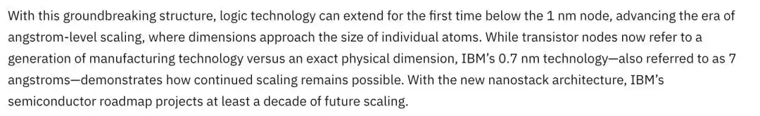
IBM's semiconductor roadmap predicts that with the NanoStack architecture, chip scaling can continue for at least another decade.

References:

[1]https://newsroom.ibm.com/2026-06-25-ibm-debuts-worlds-first-sub-1-nanometer-chip-technology

This article is from the WeChat public account "QbitAI", author: Meng Chen

Trending Cryptos

Related Questions

QWhat is the name of the new architecture that enabled IBM's 0.7nm chip breakthrough?

AThe new architecture is called 'NanoStack'. It is the industry's first three-dimensional, vertically stacked transistor design based on nanosheets.

QAccording to the article, what is a key challenge that the improved energy efficiency of the 0.7nm process aims to solve?

AIt aims to address the growing AI compute power consumption, which is evolving from a technical issue into an infrastructure problem. This is because some data center projects face construction delays due to insufficient power supply, and users want higher performance without significantly higher electricity bills.

QHow does IBM's 0.7nm chip compare to a 2nm chip in terms of performance or energy efficiency?

ACompared to a 2nm process, the 0.7nm technology offers a choice: it can provide either a 50% performance improvement or a 70% increase in energy efficiency.

QWhat significant milestone does the 0.7nm (7 Angstrom) transistor represent in semiconductor manufacturing?

AIt represents the first time a human-made transistor has broken the 1-nanometer threshold, bringing its scale close to that of individual atoms (0.1-0.5 nanometers).

QWhat is IBM's estimated timeline for the NanoStack technology to reach mass production?

AIBM's timeline suggests that the NanoStack technology could enter mass production as early as within the next five years.

Related Reads

Video Edition Nano Banana Arrives: Built-in Gemini World Knowledge, Original Banana Generates Images in Just 4 Seconds

Google has unveiled two new multimodal AI models: Gemini Omni Flash and Nano Banana 2 Lite. Gemini Omni Flash is a video generation and editing model that leverages Gemini's world knowledge. It allows for conversational video editing using natural language prompts, maintains scene consistency, and integrates text/graphics with video actions. Priced at $0.10 per second of output, its current limitations include a 10-second video cap. Nano Banana 2 Lite (gemini-3.1-flash-lite-image) is an optimized image generation model focused on speed and cost. It produces a 1K resolution image in about 4 seconds at a cost of roughly $0.034, making it significantly faster and cheaper than its predecessor. It retains strong text rendering capabilities. A key highlight is the combined workflow: users can rapidly generate images with Nano Banana 2 Lite and then seamlessly feed them into Gemini Omni Flash to create videos. Google demonstrated this with three application demos: "Anywhere" for creating travel videos from photos, "Space Lift" for generating interior design walkthroughs, and "Omni Product Studio" for automating e-commerce ad creation from product photos. The release underscores Google's strategic focus on advancing multimodal AI for practical, commercial applications in areas like marketing, design, and content creation, despite competitive pressures in other AI domains.

marsbit8m ago

Video Edition Nano Banana Arrives: Built-in Gemini World Knowledge, Original Banana Generates Images in Just 4 Seconds

marsbit8m ago

Just Now, Anthropic Released Sonnet 5, Performance Close to Opus 4.8, but Not Necessarily Cheaper

Anthropic has officially released Claude Sonnet 5, describing it as the most "agentic" Sonnet model to date. It can plan, use tools like browsers and terminals, and autonomously perform tasks at a level previously requiring larger, more expensive models. Performance in reasoning, tool use, programming, and knowledge work has significantly improved compared to Sonnet 4.6, now approaching that of Opus 4.8. Evaluation results indicate that Sonnet 5, at medium "effort" levels, offers better cost efficiency than its predecessor. At higher effort levels, its performance in some tasks can match Opus 4.8. In terms of safety, Sonnet 5 shows improved rates of refusing malicious requests and resisting prompt injection attacks compared to Sonnet 4.6, though it has a slightly higher rate of policy-violating behavior than Opus 4.8 and Mythos Preview. Its cybersecurity capabilities remain weaker than those models. Notably, Sonnet 5 uses a new tokenizer. The same text input now results in approximately 1.0 to 1.35 times more tokens, depending on content. To offset this, Anthropic offers a promotional launch price until August 31, 2026, at $2 per million input tokens and $10 per million output tokens. The standard pricing will be $3/$15 per million tokens thereafter. However, some external analysis suggests that due to increased token usage, the actual cost per task for Sonnet 5 may be higher than both Sonnet 4.6 and Opus 4.8.

marsbit1h ago

Just Now, Anthropic Released Sonnet 5, Performance Close to Opus 4.8, but Not Necessarily Cheaper

marsbit1h ago

Trading

Spot

Hot Articles

How to Buy CHIP

Welcome to HTX.com! We've made purchasing USD.AI (CHIP) simple and convenient. Follow our step-by-step guide to embark on your crypto journey.Step 1: Create Your HTX AccountUse your email or phone number to sign up for a free account on HTX. Experience a hassle-free registration journey and unlock all features.Get My AccountStep 2: Go to Buy Crypto and Choose Your Payment MethodCredit/Debit Card: Use your Visa or Mastercard to buy USD.AI (CHIP) instantly.Balance: Use funds from your HTX account balance to trade seamlessly.Third Parties: We've added popular payment methods such as Google Pay and Apple Pay to enhance convenience.P2P: Trade directly with other users on HTX.Over-the-Counter (OTC): We offer tailor-made services and competitive exchange rates for traders.Step 3: Store Your USD.AI (CHIP)After purchasing your USD.AI (CHIP), store it in your HTX account. Alternatively, you can send it elsewhere via blockchain transfer or use it to trade other cryptocurrencies.Step 4: Trade USD.AI (CHIP)Easily trade USD.AI (CHIP) on HTX's spot market. Simply access your account, select your trading pair, execute your trades, and monitor in real-time. We offer a user-friendly experience for both beginners and seasoned traders.

2.0k Total ViewsPublished 2026.04.21Updated 2026.06.02

How to Buy CHIP

Discussions

Welcome to the HTX Community. Here, you can stay informed about the latest platform developments and gain access to professional market insights. Users' opinions on the price of CHIP (CHIP) are presented below.

活动图片