In March 2026, Iran attacked a liquefied natural gas (LNG) facility in Ras Laffan, Qatar. This sparked widespread concern about the potential significant impact on the supply of helium (He), a byproduct of LNG production.
Around the same time, Iran blocked the Strait of Hormuz, causing chaos in energy logistics. In April 2026, it was reported that more than 600 vessels, including 325 oil tankers, were stranded near the strait; subsequently, about 2000 vessels were stuck in the Persian Gulf. Many of these tankers are believed to be carrying helium and naphtha, the latter being a consumable for various semiconductor manufacturing equipment and a raw material for photoresist.
Given the above scenario, the possibility of global semiconductor fabs shutting down due to the triple blow of "helium shortage," "naphtha shortage," and "photoresist shortage" has become a major concern. This article explores the reasons by tracing the supply chains of helium, naphtha, and photoresist, and discusses future prospects.
Overall Picture of the Crisis Involving Front-End Fab Shutdowns
First, let's outline the use of helium in semiconductor front-end processes and the use of naphtha-derived components and materials (Figure 1).
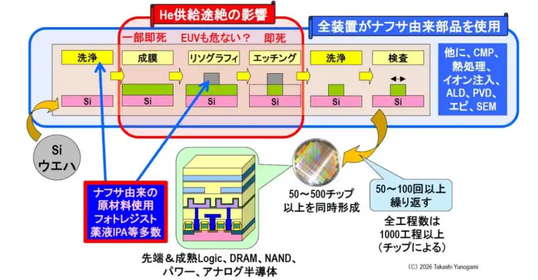
Figure 1: At which points in the process flow shown above is helium used? And where are naphtha-derived components and materials used?
In the front-end process, a series of steps including cleaning, thin-film deposition, lithography, dry etching, cleaning, and inspection are repeated 50 to 100 times or more on a silicon (Si) wafer, thereby simultaneously forming tens to hundreds of chips. Depending on the chip, the total number of steps may exceed 1000. This applies not only to advanced logic but to all semiconductor devices, including mature logic, DRAM, NAND flash, power, and analog.
The following two points are crucial.
First, if helium supply is disrupted, some thin-film deposition processes and dry etching will become impossible, leading to "instant failure," and extreme ultraviolet (EUV) lithography may also be at risk.
Second, all equipment from cleaning and thin-film deposition to lithography, dry etching, and inspection uses consumable parts derived from naphtha, and the raw materials for chemicals like photoresist and isopropyl alcohol are also naphtha-derived.
In other words, both helium (He) and naphtha can be considered the "Achilles' heel" of semiconductor front-end processes.
Front-End Processes Dependent on Helium, Especially Dry Etching
Figure 2 shows the degree of impact on various processes if helium supply is disrupted. Dry etching is the most severely affected, with a risk level of "extremely high," meaning the process itself becomes infeasible ("instant failure"). Next, single-wafer high-precision chemical vapor deposition (CVD), narrow-temperature-window edge atomic layer deposition (ALD), strict temperature-controlled sputtering, and edge epitaxial growth are all at "high" risk, leading to degradation in film thickness, film quality, stress, and crystallinity. On the other hand, batch furnace CVD and general ALD can proceed with only minor condition adjustments.
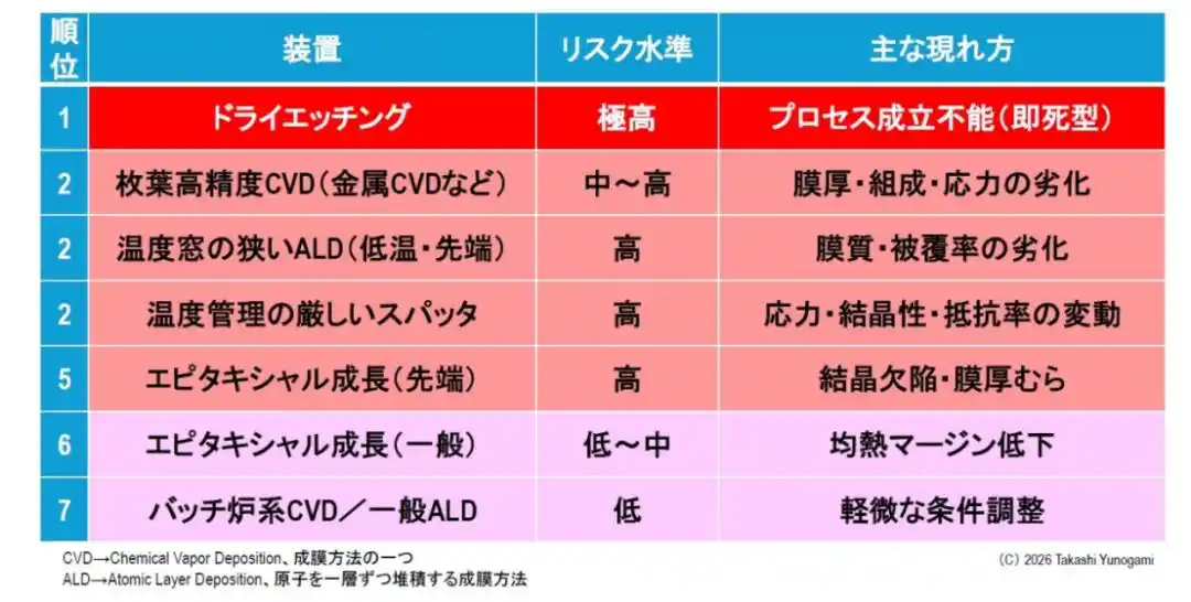
Figure 2: The degree of impact of helium supply disruption on various front-end processes.
So why does dry etching lead to instant failure? The reason lies in the principle of wafer temperature control (Figure 3). In dry etching equipment, a large amount of heat is transferred from the plasma to the wafer. Therefore, a coolant (e.g., -60°C) needs to be circulated inside the electrostatic chuck of the wafer stage to cool the wafer (the temperature of this coolant varies, ranging from below -100°C to above +100°C, and is optimized for each process).
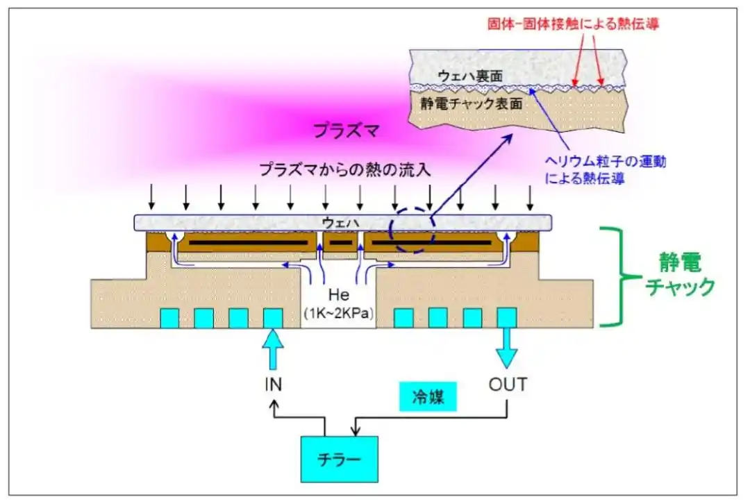
Figure 3. Principle of temperature control in a dry etching apparatus.
However, on a microscopic level, there is only one contact point between the electrostatic chuck and the backside of the wafer, so cooling via coolant circulation alone is insufficient. Therefore, helium (He) gas at 1-2 kPa is injected into the gap between the electrostatic chuck and the wafer. Because helium is a light monatomic molecule with extremely fast movement, it effectively transfers heat from the wafer to the electrostatic chuck. Afterwards, this helium gas is exhausted by vacuum pumps. In other words, it's "single-use."
Put simply, without helium, wafer temperature control is impossible, and the dry etching process itself cannot proceed. Not only low-temperature etching processes like deep hole drilling for 3D NAND become impossible, but all dry etching processes fail. This is what is meant by "instant failure."
Naphtha-Related Equipment Parts and Photoresist
What about naphtha? All consumables in semiconductor manufacturing equipment use naphtha-derived parts and materials, including: (1) High-performance resins; (2) Rubbers and elastomers, such as O-rings; (3) Plasma-resistant and chemically resistant fluorine-based materials; (4) Fluid components, such as pipes and valves; and (5) Cables and insulating materials. Since manufacturing equipment requires regular replacement of consumables to maintain stable operation, depletion of parts inventory directly leads to equipment downtime, which in turn leads to fab-wide shutdowns.
Another serious issue is photoresist. The production process for photoresist is: naphtha → propylene → propylene oxide (PO) → PGME → PGMEA → photoresist (Note). Five Japanese companies (Tokyo Ohka Kogyo Co., Ltd., JSR, Shin-Etsu Chemical Co., Ltd., FUJIFILM, and Sumitomo Chemical Co., Ltd.) dominate over 90% of the global photoresist market, and these five companies source almost all of their PGME and PGMEA from the Japanese manufacturer Daicel Corporation. If any part of this supply chain is disrupted, global semiconductor fabs would shut down.
So, why haven't semiconductor fabs shut down? Let's first look at naphtha production. Figure 4 shows naphtha production by region. Globally, about 1 billion tonnes of naphtha are produced annually, with about 18% (about 180 million tonnes) coming from the Middle East. Of this 1 billion tonnes, about 600 million tonnes are used as ethylene feedstock, about 200 million tonnes as gasoline blending stock, and about 100 million tonnes for BTX (benzene, toluene, xylene). Less than 1 million tonnes, or less than 0.1% of global naphtha, is used to produce semiconductor materials like PGME, PGMEA, and photoresist.
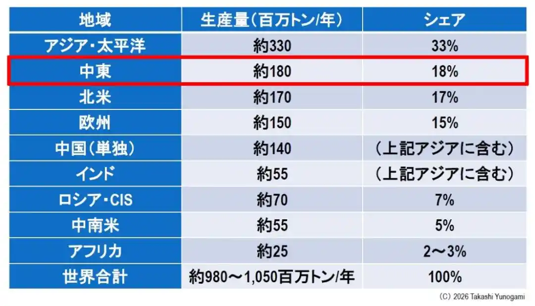
Figure 4. Regional and global naphtha production (2025-2026). Source: Author's estimation based on global refining capacity, crude processing volume, and naphtha yield (~15-20%).
Therefore, even if a blockade of the Strait of Hormuz causes a naphtha shortage, Daicel and photoresist manufacturers can prioritize securing this minuscule amount of naphtha for semiconductor materials. Since the proportion of naphtha used for photoresist is extremely small, this structure makes it easier to secure the supply of semiconductor materials.
The situation for helium (He) is completely different. As shown in Figure 5, global annual helium production is 190 million cubic meters, with the United States accounting for 42.6% and Qatar for 33.2%. A disruption in Qatar's helium supply would mean losing one-third of the global supply. Furthermore, the semiconductor industry is estimated to consume about 21% to 24% of global helium, or 39 million to 46 million cubic meters annually. Qatar's annual helium supply of 63 million cubic meters exceeds the total annual consumption of the global semiconductor industry. Even a simple quantitative comparison reveals the enormity of the impact.
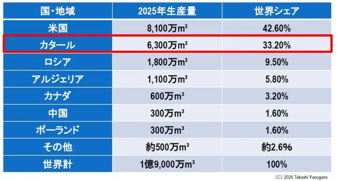
Figure 5. Regional and global helium production (2025). Source: U.S. Geological Survey (USGS) 2026 data.
However, semiconductor fabs have not shut down for three reasons.
First, "reserves" are key; gas producers like Linde, Air Liquide, Air Products, and Iwatani have stockpiled a certain amount of gas, which helps absorb the initial shock.
Second, regarding "inventory and recycling", companies have increased their inventories based on past helium shortage experiences, and TSMC and Samsung Electronics have already implemented helium recovery systems (though not entirely).
Third, according to "priority supply rules", the order of priority is medical → aerospace/defense → semiconductor industry → general industry → balloons, with balloons and general industrial supplies being the first to be cut.
However, helium (He) cannot be stored for long periods. Liquid helium must be stored at ultra-low temperatures below -269°C, and about 1% of the helium is lost daily due to evaporation. Therefore, without timely replenishment, helium reserves will fall below 75% in 30 days, below 50% in 70 days, and below 10% in 230 days. Furthermore, transporting liquid helium requires specialized ISO containers, of which there are only a few hundred globally.
Additionally, helium inventories at semiconductor fabs last only days to weeks, while those at gas companies and logistics centers last weeks to months, meaning that even using all available resources can only sustain supply for about six months at most. In other words, the risk of helium supply disruption is far greater than that of a naphtha-derived photoresist shortage. The current helium crisis is not resolved; it's merely delayed.
Impact on Logic Semiconductors
If a helium (He) supply disruption persists for too long, the most affected will be cutting-edge logic devices. The formation of GAA (Gate-All-Around nanosheet structure) for 2nm processes (N2) involves numerous processes requiring precise temperature control, such as multilayer epitaxial growth of Si and SiGe, selective plasma etching of sacrificial SiGe layers, and atomic layer deposition (ALD) of inner spacers (Figure 6). Among these, plasma etching of SiGe is the most difficult process and is inseparable from helium. In other words, without helium, GAA processing itself becomes impossible.
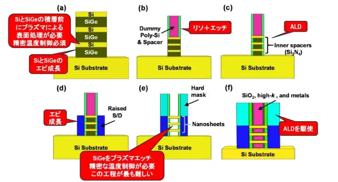
Figure 6. Multiple steps in GAA nanosheet formation require precise temperature control. Source: Adapted and annotated by Takashi Yunogami from IBM Research's nanosheet GAA process flow diagrams (IEDM 2019-2021), with additions by the author.
Figure 7 shows the impact of helium supply disruption on logic semiconductor nodes and the predicted fab shutdown times. Next-generation cutting-edge logic chips like A14 and N2, produced by companies like TSMC, Samsung, Intel, and Rapidus, are impacted "extremely severely," causing fabs to shut down immediately or within three months of a helium supply halt. N3 chips will also shut down within three months, while N5 and N7 chips will shut down within six months.
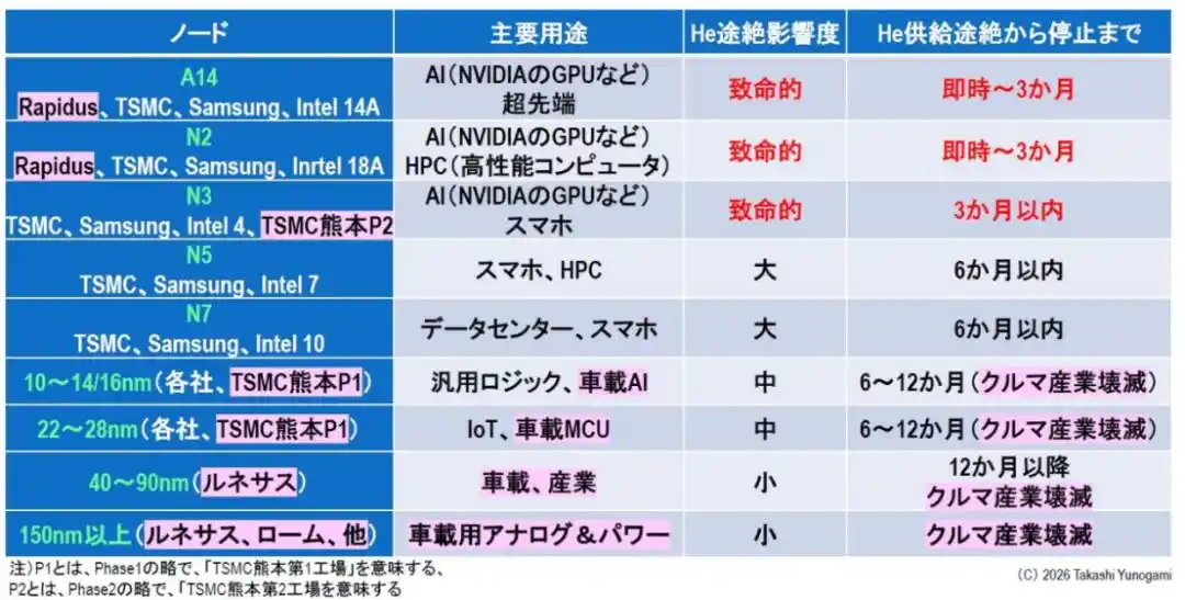
Figure 7. Logic semiconductor nodes, main applications, and predicted semiconductor fab shutdown times (pink indicates Japanese semiconductor fabs, their main applications, and relation to the automotive industry).
Particularly noteworthy are mature nodes: 10-28nm (including TSMC's Kumamoto Fab 1) will shut down in 6-12 months, and automotive, analog, and power semiconductors (40nm and above) from companies like Renesas and Rohm will also shut down after 12 months, all of which could lead to "destruction of the automotive industry."
This is because, even at mature process nodes, automotive semiconductor qualification standards are extremely stringent, and automakers will not accept chips manufactured without helium-based dry etching. In other words, the risk of helium supply disruption is not just for cutting-edge technology.
If Qatar's helium supply remains at zero, how long can the semiconductor industry survive?
For the initial 0-3 months, the situation can be managed through inventories, underground storage, increased flights from the U.S., and reallocation among different uses; while prices will skyrocket, major semiconductor fabs will continue operations.
Within 3 to 6 months, quota cuts will begin, starting with non-contract users, small fabs, research institutions, back-end processes, and general products.
In the subsequent 6 to 12 months, partial operational restrictions (including for advanced fabs) will become a reality, placing a particularly heavy burden on Asian countries like South Korea, China, and Japan that rely on long-distance imports of liquid helium.
If the shortage persists for over a year, unless increased production from countries like the U.S., Canada, Algeria, and Russia can fill the 33% gap, the semiconductor industry will be forced to prioritize which products to produce.
This indicates that this crisis will not lead to all semiconductor fabs shutting down simultaneously, but will unfold quietly in the following sequence: rationing → significant price hikes → reduced production of older, low-margin products → partial shutdowns by region and company.
*Disclaimer: This article was created by the original author. The content represents the author's personal views. We republish it for sharing and discussion purposes only and do not necessarily endorse or agree with the views expressed. For any objections, please contact us.
This article is from the WeChat public account "Semiconductor Industry Vertical and Horizontal" (ID: ICViews), author: Yunogami Takashi