# EDA İlgili Makaleler

HTX Haber Merkezi, kripto endüstrisindeki piyasa trendleri, proje güncellemeleri, teknoloji gelişmeleri ve düzenleyici politikaları kapsayan "EDA" hakkında en son makaleleri ve derinlemesine analizleri sunmaktadır.

SemiAnalysis Dissects Huawei's Kirin 9030: Process Technology Halted, So They Folded the Chip

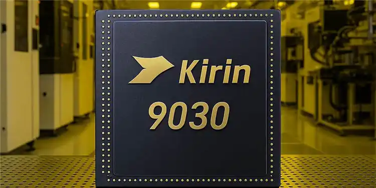
SemiAnalysis has published a detailed teardown report on the HiSilicon Kirin 9030 Pro chipset found in Huawei's Mate 80 Pro. Fabricated using SMIC's most advanced N+3 node without EUV lithography, the analysis reveals significant technical achievements and strategic shifts. The report indicates SMIC's N+3 has achieved transistor density comparable to TSMC's N6 (113.4 vs 107.7 MTr/mm²), primarily through aggressive use of Self-Aligned Quadruple Patterning (SAQP) for its metal layers. This results in a notably small 32.5nm M0 metal pitch. However, SemiAnalysis notes this achievement comes with significantly higher process complexity, cost, and potential yield challenges compared to competitors using more advanced tools. The Kirin 9030 design maximizes this constrained density. While its GPU performance has improved ~70% and matches Qualcomm's 2022 flagship level, the CPU core's IPC lags behind current top-tier designs from Apple and Qualcomm, a gap attributed to the underlying manufacturing technology rather than design capability. Facing long-term restrictions on advanced tools, Huawei is charting a new path. The report highlights the company's "LogicFolding" roadmap, a 3D stacking technique aimed at shortening signal paths to boost performance and efficiency. The goal is to reach 5GHz frequency and a projected density of 295 MTr/mm² by 2031. SemiAnalysis concludes that export controls have not halted China's chip progress but have fundamentally altered its trajectory, making it more expensive and complex. This has spurred innovation in alternative areas like 3D stacking and domestic EDA tool development, with Huawei's supply chain also beginning to integrate Chinese memory from CXMT.

marsbit06/15 06:52

SemiAnalysis Dissects Huawei's Kirin 9030: Process Technology Halted, So They Folded the Chip

marsbit06/15 06:52

The Tao (τ) Law Makes EDA Go Viral

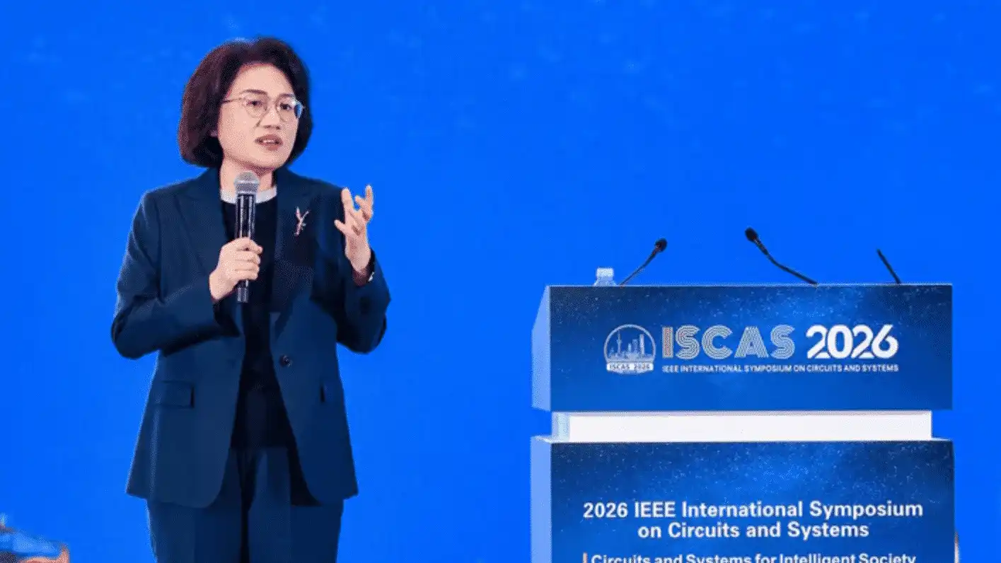
In May 2026, Huawei's semiconductor division introduced the "Tao (τ) Law" at IEEE ISCAS, shifting the industry focus from Moore's Law's geometric scaling to "time scaling." Unlike traditional approaches relying on transistor miniaturization, τ Law optimizes the time constant (τ) across device, circuit, chip, and system levels to improve information processing speed and efficiency. Huawei has already applied this principle, mass-producing 381 chips across various applications, with a target to achieve performance equivalent to 1.4nm technology by 2031. The implementation of τ Law, involving techniques like Chiplet, 3DIC, and Logic Folding, places new demands on EDA tools, highlighting gaps in current offerings. Traditional 2D or pseudo-3D EDA flows lack native support for true 3D design, cross-layer co-optimization (STCO), and coupled multi-physics analysis (thermal, power, stress), which are crucial for advanced integration. Chinese EDA companies, such as Empyrean Software, Primarius Technologies, and Xpeedic, are evolving from point-tool specialists to providing full-flow, system-level solutions. For instance, Peking University has developed a prototype "true 3D" EDA tool showing significant improvements in wirelength and timing. Empyrean Software has also launched a comprehensive 3DIC design and verification platform. The τ Law framework presents an opportunity for the domestic EDA industry to transition from achieving basic functionality to developing robust, integrated toolsets essential for next-generation chip design.

marsbit06/12 13:39
The Tao (τ) Law Makes EDA Go Viral

marsbit06/12 13:39

Huawei's "Tao Law": A Comprehensive Overview of Core Companies

Huawei's "Tau Law": Core Companies Overview On May 25, 2026, Huawei's Director and President of the Semiconductor Business Division, He Tingbo, formally introduced the "Tau (τ) Law" at ISCAS 2026, marking a significant principle guiding industry development in the global semiconductor field from China. The Tau Law shifts focus from traditional Moore's Law, which pursues geometric transistor scaling, to "time scaling"—continuously compressing signal propagation delay (time constant τ) without solely relying on extreme feature size reduction. The core implementation path is "logic folding." This technique transforms circuit layouts from two-dimensional planes to multi-layer 3D stacks, using short vertical interconnects to replace long horizontal wiring, thereby drastically reducing τ. Huawei has already designed and mass-produced 381 chips following this principle over the past six years, with plans to launch a Kirin chip utilizing logic folding in Fall 2026. By 2031, high-end chips based on the Tau Law are expected to achieve performance levels equivalent to a 1.4nm process node. This development impacts several key industry segments, with related Chinese companies poised to benefit: 1. **EDA Design Software**: Essential for circuit-level optimization. Key players include: * **Empyrean Technology** (Huada Jiutian): China's largest full-flow EDA provider. * **Primarius Technologies** (Gailun Dianzi): Specializes in device modeling and verification. * **Semitronix** (Guangliwei): Focuses on yield enhancement and test chip EDA. 2. **Chiplet & Advanced Packaging**: Logic folding's 3D stacking necessitates advanced packaging (e.g., TSV, hybrid bonding). Core participants are: * **Tongfu Microelectronics**: A leader in advanced packaging and a key partner for AMD's Chiplet products. * **JCET Group** (Changdian Keji) & **Tianshui Huatian Technology**: Major OSATs with advanced packaging capabilities. * **VeriSilicon** (Xinyuan Gufen): Provides Chiplet-based design platforms and IP. 3. **Foundry Manufacturing**: Optimization must be implemented in transistor structures and process parameters. Potential foundries for Huawei's future chips include: * **SMIC**: China's leading foundry with advanced FinFET capabilities, the most likely candidate for next-gen Kirin chips. * **Hua Hong Semiconductor** (Huahong Gongsi): A leader in specialty processes (power, embedded memory). * **Nexchip Semiconductor** (Jinghe Jicheng): Major foundry for display driver ICs and MCUs. The Tau Law represents a strategic move towards architectural innovation and design-process co-optimization, driving demand across the domestic semiconductor supply chain.

marsbit05/25 11:33

Huawei's "Tao Law": A Comprehensive Overview of Core Companies

marsbit05/25 11:33

活动图片