Farewell to the Copper Era: Understanding the Logic of the AI Silicon Photonics Industry Chain and Key US Stock Players

marsbitОпубликовано 2026-05-19Обновлено 2026-05-19

Введение

**Summary: The Era of Silicon Photonics and Key AI Infrastructure Stocks** The article delves into the transition from copper-based interconnects to silicon photonics (SiPh) as a critical enabler for next-generation AI data centers. It explains that copper faces fundamental physical limits—the bandwidth wall, density wall, and power wall—at high data rates (1.6T+), making a material shift essential. Silicon photonics, which integrates components like lasers, modulators, and detectors onto a silicon chip, offers a solution by leveraging mature CMOS manufacturing for cost-effective, high-volume production. A key challenge is that silicon itself is not an efficient light source, making Indium Phosphide (InP) lasers a critical and supply-constrained component. A major industry catalyst was NVIDIA's 2025 GTC announcement, declaring optical interconnects a "standard" from its Rubin platform onward, followed by strategic investments to secure the supply chain. The industry is structured in four key layers: 1. **Foundries:** TSMC leads with its COUPE platform, while Tower Semiconductor (specialized SiPh foundry) and GlobalFoundries are major players. 2. **Core Component Suppliers:** Lumentum is highlighted as the sole volume manufacturer of the crucial 200G/lane EML laser, with orders locked by NVIDIA through 2027. 3. **Module & System Manufacturers:** Coherent holds significant market share, with Chinese manufacturers like InnoLight also noted for scale. 4. **System Integrato...

Author: Godot

The two hottest sectors in AI are storage and photonics. Previously, I wrote a framework on storage (Understanding the Profit Pools and Industry Landscape of AI Storage Tiers). This article focuses on photonics.

Silicon photonics (Silicon Photonics) is used for communication between computing chips, replacing traditional copper wires, as clearly shown in the diagram below.

Terms you might come across but find confusing, such as LPO (Linear-drive Pluggable Optics), CPO (Co-packaged Optics), OCS (Optical Circuit Switching), and Optical I/O (Optical Input/Output), represent different technical approaches to implementing silicon photonics.

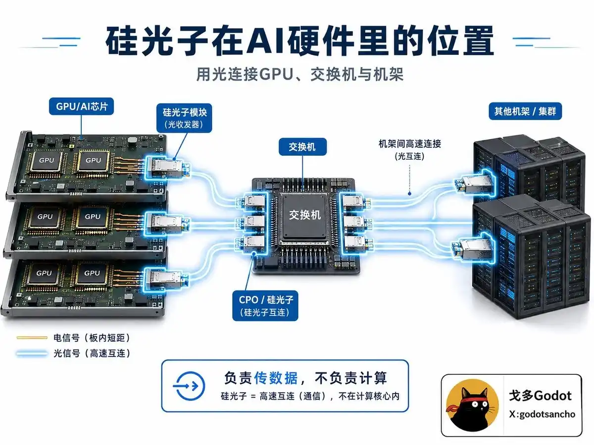
Typically, chips communicate using copper wires. Silicon photonic chips integrate components like lasers (which generate light), modulators (which "modulate" light), and *detectors* (which "receive" light) directly onto silicon wafers, enabling communication via photons.

So, why replace copper? And why use silicon photonics instead of other alternatives?

First, copper wires nearly reach their physical limits when transmitting signals above 1.6T, leading to signal degradation. Switching materials becomes imperative. This is the most critical issue and a necessary change. The technical term is the "bandwidth wall."

Second, copper is a tangible physical entity. As GPU clusters expand, there simply isn't enough space for all the copper wiring. This is another compelling reason to replace copper. Photonics are different; optical interfaces can be soldered directly next to switch chips, eliminating the need for extensive cabling. The term for this is the "scale wall."

Third, copper consumes too much power. In facilities consuming hundreds of megawatts, silicon photonics can save tens of thousands of kilowatt-hours daily—energy otherwise wasted on copper wire communication. After switching to photonics, this power can be redirected to GPUs for actual computation. This is termed the "power wall."

More interestingly, silicon photonics can leverage the mature CMOS manufacturing processes of the existing semiconductor industry, eliminating the need to build entirely new factories from scratch, thus enabling low-cost, high-volume production.

Of course, silicon photonics also has a drawback: silicon itself cannot emit light efficiently and must rely on Indium Phosphide (InP) materials. This has become the most critical bottleneck in the entire supply chain.

The Evolution of Silicon Photonics Technology

The most significant watershed moment was in March 2025 when NVIDIA, at its GTC conference, launched the Quantum-X and Spectrum-X photonic switches. Jensen Huang announced that starting from the next-generation Rubin architecture, "optical interconnect is not an option, it's a requirement."

A week later, NVIDIA announced a combined $4 billion investment in Coherent and Lumentum to secure key supply chains.

The paper on the silicon-based photoelectric effect was published in the 1980s. From 2004 to 2014, Intel and IBM manufactured silicon-based optical modulators.

In the previous decade, hyperscale cloud service providers like AWS, Google, and Meta adopted silicon photonics, though at the time it was only a part of fiber optic communication.

Current Industry Landscape

1) The Foundation: Foundries

They manufacture photonic chips. TSMC $TSM leads with its COUPE process. Tower Semiconductor $TSEM specializes in silicon photonics foundry services, with its silicon photonics revenue growing 70% year-over-year in 2025. GlobalFoundries $GFS, through its acquisition of Singapore's AMF, has become the world's largest dedicated silicon photonics foundry.

2) The Second Tier: Core Component Suppliers

They provide components like lasers and modulators, primarily Indium Phosphide (InP) lasers. Globally, fewer than five companies can manufacture high-speed EML lasers.

Lumentum $LITE is the only manufacturer capable of mass-producing 200G/lane EML lasers, a core component for 1.6T optical modules. To lock in its capacity, NVIDIA has secured orders extending beyond 2027.

3) The Third Tier: Module and System Manufacturers

They assemble components into finished products. Coherent holds about 25% of the global optical transceiver market share. Chinese companies like InnoLight, Eoptolink, and Accelink are significant contenders in terms of manufacturing scale and cost competitiveness.

4) The Top Tier: System Integrators

This layer includes NVIDIA, Cisco, Broadcom $AVGO, and Marvell $MRVL.

In summary,

NVIDIA $NVDA

Holds a dominant position, deciding the interconnect standards for AI data centers and securing supply chains through strategic investments.

Broadcom $AVGO

The absolute leader in networking switch chips, commanding nearly 80% market share in Ethernet switches. The Tomahawk 6-Davisson is the world's first 102.4 Tbps CPO switch.

Marvell $MRVL

Broadcom's strongest challenger, dominating the PAM4 optical DSP market with a 60-70% share. Recently acquired Celestial AI to enter the chip-to-chip optical interconnect space.

Lumentum $LITE

The most critical supplier of EML lasers. The world's only manufacturer capable of mass-producing 200G/lane EML lasers. NVIDIA has locked in orders until after 2027.

Coherent $COHR

An integrated player across the entire supply chain, with a presence from materials and lasers to modules. FY2025 revenue was $5.8 billion, making it the market leader in optical transceiver share.

TSMC $TSM

The process standard-setter. Its 65nm silicon photonics process is in mass production. The COUPE platform is currently the most advanced 3D heterogeneous integration solution, and NVIDIA's CPO roadmap is deeply tied to it.

Tower Semiconductor $TSEM

The purest beneficiary of the silicon photonics foundry trend. Its silicon photonics revenue grew 70% year-over-year in 2025. It is investing $650 million to triple its capacity. It has the highest potential for valuation elasticity among all the mentioned players.

Lightmatter / Ayar Labs (Unlisted · IPO Candidates)

Lightmatter, valued at $4.4 billion, focuses on 3D photonic interconnects. Ayar Labs has received investments from AMD, Intel, and NVIDIA, working on optical I/O chiplets. Both are potential major IPO candidates.

Valuation Logic Shift Driven by the Silicon Photonics Boom

Take an example. Previously, Wall Street valued Tower Semiconductor as a regular analog foundry, with a Price-to-Sales (P/S) ratio of around 2-3x.

But when its silicon photonics business grew from 5% to 30%-40% of total revenue, the market began to revalue it as a scarce asset within AI infrastructure, potentially lifting its P/S ratio to 6-10x.

Lumentum and Coherent, once viewed as telecom component suppliers, are now being redefined as indispensable providers of AI interconnect components. BofA analyst Vivek Arya raised Marvell's target price to $200, underpinned by valuing Marvell as an AI infrastructure platform rather than a communications chipmaker.

Evercore ISI's assessment of Cisco is similar. As silicon photonics products penetrate hyperscale data centers, Cisco's core AI-related revenue could potentially explode from $3 billion to $12-$15 billion over the next 3-4 years.

The Moat of the Silicon Photonics Industry

The silicon photonics industry exhibits clear winner-take-most characteristics, as every single process has been refined over a long period *before* the AI boom.

InP lasers: Globally, fewer than five companies can mass-produce high-end EML lasers, with a capacity expansion cycle of 3-5 years. This is the most critical bottleneck in the entire supply chain.

TSMC's COUPE process: The technological barrier of 3D heterogeneous integration puts competitors at least two generations behind, requiring years of yield experience accumulation.

Foundry PDK ecosystem: Once a customer designs with a specific foundry's Process Design Kit (PDK), the switching cost is extremely high—redesigning and recertification can take 12-18 months.

Thermal management and packaging: CPO requires managing the coupling of electrical, thermal, and optical domains within a few millimeters of space, which cannot be achieved without years of system integration experience.

The supplier certification process for giants like AWS and Google typically takes 12-24 months. Once certified, customer stickiness is extremely strong.

Risks and Cold-headed Considerations

The growth of the entire industry chain is highly dependent on the capital expenditures of the five hyperscale cloud giants: Microsoft, Google, Meta, Amazon, and Oracle.

There is substitutability among technical paths like LPO, CPO, OCS, and Optical I/O. If one route is disrupted by another, previously invested capital may face depreciation or write-downs.

Research firms like LightCounting judge that truly large-scale CPO deployment will not arrive until after 2028. Before that, transitional solutions like LPO will dominate volumes.

Therefore, betting on the success of the *industry* is safer than betting on the success of a *single company*.

Связанные с этим вопросы

QAccording to the article, what are the three major limitations (or 'walls') of using copper interconnects in high-performance AI systems that silicon photonics aims to overcome?

AThe article outlines three major limitations of copper: 1) The Bandwidth Wall: Copper wires hit a physical limit for transmitting signals above 1.6T, leading to signal degradation. 2) The Scale Wall: As GPU clusters grow, physical copper wiring takes up too much space, whereas optical interfaces can be placed directly next to switch chips. 3) The Power Wall: Copper interconnects consume significant power, with silicon photonics potentially saving tens of thousands of kilowatt-hours per day in large facilities, freeing up power for GPUs to compute.

QWhy is Indium Phosphide (InP) a critical 'chokepoint' in the silicon photonics supply chain?

AInP is a critical chokepoint because silicon itself is not an efficient light emitter. High-performance lasers, particularly the essential Electro-absorption Modulated Lasers (EML) needed for high-speed data transmission, are made from Indium Phosphide. The article states there are fewer than five companies globally capable of manufacturing high-end EML lasers, and capacity expansion takes 3-5 years.

QName two companies positioned in the 'Core Components Supplier' layer of the silicon photonics industry chain as described in the article and explain their key advantage.

ATwo companies in the core components layer are Lumentum (LITE) and Coherent (COHR). Lumentum's key advantage is being the world's only company capable of mass-producing the 200G/lane EML laser, a core component for 1.6T optical modules, with NVIDIA having locked in its capacity through 2027. Coherent, as a full-industry-chain integrator, holds about 25% of the global optical transceiver market share, with a strong position from materials to modules.

QHow is the valuation logic changing for companies like Tower Semiconductor due to the rise of AI silicon photonics?

APreviously, Tower Semiconductor (TSEM) was valued as an ordinary analog foundry with a price-to-sales ratio of 2-3x. As its silicon photonics business is forecasted to grow from 5% to potentially 30-40% of revenue, the market is beginning to revalue it as a scarce AI infrastructure asset. This could push its price-to-sales ratio to a range of 6-10x.

QWhat is one major risk factor highlighted for the silicon photonics industry's growth, aside from dependence on hyperscaler capital expenditure?

AA major risk factor is technological substitution. Different technical paths like LPO, CPO, OCS, and Optical I/O are competing. If one technology path is ultimately displaced by another, the capital invested in the former could face depreciation and impairment risks.

Похожее

Jensen Huang: Vera Rubin Full Mass Production, AI Agent a Key Focus, Challenging Intel to Target the Next-Generation AI PC Gateway

NVIDIA CEO Jensen Huang delivered the keynote speech at GTC Taipei 2026, announcing several major product launches and strategic directions. The company's Vera Rubin architecture is now in full-scale production, with OpenAI, Anthropic, and SpaceX among the first customers. NVIDIA highlighted AI Agent as a key future focus, introducing the Vera CPU designed for AI agents and the Vera BlueField-4 STX for secure, chip-level AI storage processing. A significant move involves challenging Intel in the PC market. NVIDIA, in collaboration with MediaTek, is developing the RTX SPARK PC chip (manufactured by TSMC) for Windows systems, set to launch this fall for laptops and desktops. This signals NVIDIA's push into the next-generation AI PC arena, aiming to provide a vertically integrated core computing platform for the entire Windows ecosystem, similar to Apple's approach. Other announcements include the new Nemotron 3 Ultra AI model and the NVIDIA DSX platform, described as a complete "playbook" for building AI factories, allowing performance simulation and validation before physical deployment. In automotive, the DRIVE Hyperion platform was positioned as a global robotaxi platform, with major Chinese automakers like BYD, Geely, Zeekr, Xiaomi, and Pony.ai already adopting or developing autonomous driving solutions based on it. The Alpamayo 2 super open inference model for robotaxis was also introduced. For robotics, NVIDIA unveiled the Isaac GR00T humanoid robot reference platform for academic research and a large open-source agent tools and skills suite for Physical AI. The company plans to collaborate with global humanoid robot manufacturers, including China's Unitree, whose H2 Plus robot served as the reference hardware for the GR00T platform demonstration.

marsbit12 мин. назад

Jensen Huang: Vera Rubin Full Mass Production, AI Agent a Key Focus, Challenging Intel to Target the Next-Generation AI PC Gateway

marsbit12 мин. назад

Running MoE on Mobile Phones? Meta Proposes MobileMoE, Speeding Up iPhone 16 Pro by 3.8x

Meta's MobileMoE, a mobile-optimized Mixture-of-Experts (MoE) language model architecture, enables efficient on-device large language model (LLM) inference for the first time on commercial smartphones. Designed for decoder-only Transformers, it replaces dense feed-forward layers with MoE layers. Key design choices include 8 experts with granularity g=8, top-4 routing, and a shared expert. The model undergoes a four-stage training process: pre-training, intermediate training, supervised fine-tuning, and quantization-aware training. Results show MobileMoE models, with similar memory footprint, achieve equal or higher average accuracy across 14 foundational benchmarks while using only 1/2 to 1/4 of the FLOPs compared to dense baselines. After INT4 quantization, they remain competitive. Notably, on an iPhone 16 Pro, MobileMoE-S demonstrates significant speedups: up to 3.8x faster in the prompt phase and 2.2-3.4x faster in per-token generation compared to a dense counterpart, with lower peak memory usage. While MobileMoE establishes a new Pareto frontier for on-device LLMs in accuracy-compute trade-offs, particularly excelling in code and math tasks, it currently lags behind models like Qwen3.5 2B in advanced instruction following and knowledge reasoning. Future work includes improving post-training techniques, exploring NPU deployment, and managing the runtime memory sensitivity of MoE models to varying inputs.

marsbit16 мин. назад

Running MoE on Mobile Phones? Meta Proposes MobileMoE, Speeding Up iPhone 16 Pro by 3.8x

marsbit16 мин. назад

Bitcoin's Weak Rebound Fails to Mask Adjustment Trend, HYPE's Top Signal Warns of Short-Term Risks | Invited Analysis

**Title:** Bitcoin's Weak Rebound Fails to Mask Downtrend; HYPE Top Signal Alerts of Short-Term Risks | Exclusive Analysis **Abstract:** This weekly market analysis examines the current technical structures of Bitcoin and HYPE, outlining key trading strategies. Bitcoin's daily chart shows it has broken below the median line of its primary ascending channel, indicating structural weakness. It is currently experiencing a weak rebound within a short-term descending channel, targeting resistance at $75,000-$76,000. Failure to break above this zone could lead to a resumption of the downtrend, testing support at $69,500-$70,500. Trading strategies include positioning for a rebound rejection (Plan A) or a breakdown below key support (Plan B) with controlled short positions. For HYPE, the 4-hour chart reveals a potential seven-wave advance from the May 14 low, now showing signs of exhaustion. A bearish divergence (momentum weakening) has been observed, coupled with a top signal from the proprietary "Spread Trading Model" at potential endpoint 47. The key this week is to monitor if a confirmed top forms here, especially upon a breach of the $62.5-$64.57 support area. If broken, a larger corrective move towards $54-$56.30 is anticipated. The short-term strategy for HYPE focuses on cautious long entries only upon confirmed stabilization within the support zone. The report also details a successful short BTC trade from the previous week, yielding a ~5.07% profit, executed based on model signals and price action. Strict risk management rules, including dynamic stop-loss adjustments, are emphasized.

marsbit32 мин. назад

Bitcoin's Weak Rebound Fails to Mask Adjustment Trend, HYPE's Top Signal Warns of Short-Term Risks | Invited Analysis

marsbit32 мин. назад

Торговля

Спот
Фьючерсы

Популярные статьи

Как купить ERA

Добро пожаловать на HTX.com! Мы сделали приобретение Caldera (ERA) простым и удобным. Следуйте нашему пошаговому руководству и отправляйтесь в свое крипто-путешествие.Шаг 1: Создайте аккаунт на HTXИспользуйте свой адрес электронной почты или номер телефона, чтобы зарегистрироваться и бесплатно создать аккаунт на HTX. Пройдите удобную регистрацию и откройте для себя весь функционал.Создать аккаунтШаг 2: Перейдите в Купить криптовалюту и выберите свой способ оплатыКредитная/Дебетовая Карта: Используйте свою карту Visa или Mastercard для мгновенной покупки Caldera (ERA).Баланс: Используйте средства с баланса вашего аккаунта HTX для простой торговли.Третьи Лица: Мы добавили популярные способы оплаты, такие как Google Pay и Apple Pay, для повышения удобства.P2P: Торгуйте напрямую с другими пользователями на HTX.Внебиржевая Торговля (OTC): Мы предлагаем индивидуальные услуги и конкурентоспособные обменные курсы для трейдеров.Шаг 3: Хранение Caldera (ERA)После приобретения вами Caldera (ERA) храните их в своем аккаунте на HTX. В качестве альтернативы вы можете отправить их куда-либо с помощью перевода в блокчейне или использовать для торговли с другими криптовалютами.Шаг 4: Торговля Caldera (ERA)С легкостью торгуйте Caldera (ERA) на спотовом рынке HTX. Просто зайдите в свой аккаунт, выберите торговую пару, совершайте сделки и следите за ними в режиме реального времени. Мы предлагаем удобный интерфейс как для начинающих, так и для опытных трейдеров.

720 просмотров всегоОпубликовано 2025.07.17Обновлено 2025.07.17

Как купить ERA

Обсуждения

Добро пожаловать в Сообщество HTX. Здесь вы сможете быть в курсе последних новостей о развитии платформы и получить доступ к профессиональной аналитической информации о рынке. Мнения пользователей о цене на ERA (ERA) представлены ниже.

活动图片