It has to be said, the demand for optical chips is just too strong.
In recent days, a series of capacity expansion, long-term agreements, investment, and supply chain binding actions have emerged intensively across the global optical chip industry chain: Coherent is expanding its 6-inch InP compound semiconductor production line in Sherman, Texas; Nokia is expanding advanced testing and packaging capacity for photonic chips in Allentown, Pennsylvania, USA; Japan's JX Advanced Metals plans to invest up to 120 billion yen to increase InP substrate capacity by 7–10 times; IQE has reached a multi-year InP epitaxial wafer supply agreement with Tower Semiconductor; domestically, Suzhou Dongshan Precision Manufacturing's subsidiary Source Photonics also announced a photonic chip and high-speed optical module expansion project in Changzhou, with a total investment of $12 billion.
A capacity race centered on AI data center optical interconnect capabilities has already begun.
The Global Landscape of Optical Chip Company Expansions
First, let's look at the expansion moves in the United States.
On June 16, Coherent announced it had signed a letter of intent to receive up to $50 million in direct funding from the U.S. Department of Commerce under the CHIPS and Science Act to expand its world-leading 6-inch Indium Phosphide (InP) semiconductor manufacturing facility in Sherman, Texas. Immediately following the announcement the next day, Coherent held a groundbreaking ceremony for the expansion at its Sherman, Texas, plant. Coherent emphasized that this site hosts the world's first and currently largest-scale 6-inch InP manufacturing platform. Upon completion, the facility's manufacturing space will double, and wafer production capacity will increase fourfold.
Notably, NVIDIA founder and CEO Jensen Huang personally attended Coherent's ceremony, sharing the stage with Coherent's new CEO, Jim Anderson. NVIDIA had previously announced a strategic investment of $2 billion in Coherent to secure future capacity for its most advanced lasers, optical engines, and optical modules. Huang remarked at the event: "AI runs on compute, but scale is stuck on connectivity, and the Sherman factory is where these 'connectivity nerve tissues' are being built."
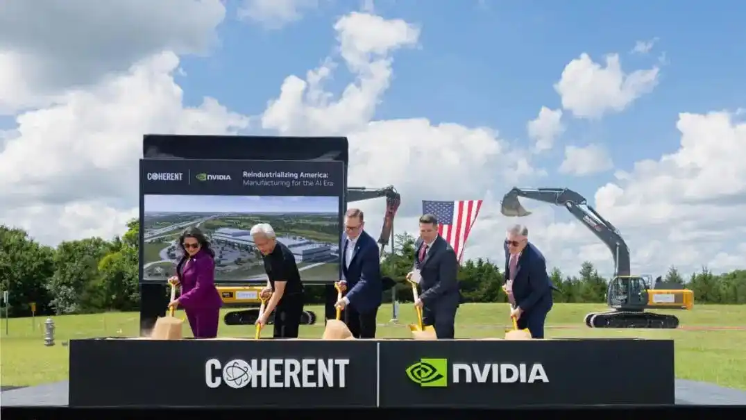
Image source: techpowerup
Nvidia has already brought "light" into the AI infrastructure supply chain with capital. As early as this March, Nvidia announced separate investments of $2 billion each in Coherent and Lumentum, accompanied by multi-year purchase commitments and future capacity/access rights, for advanced lasers, optical networking products, R&D, and US manufacturing capacity expansion.
Lumentum is also a key player in the US optical chip expansion landscape. In March, Lumentum announced it would build a new advanced laser manufacturing facility in Greensboro, North Carolina. The facility, covering approximately 240,000 square feet, will focus on producing Indium Phosphide (InP) optical devices for large global AI data centers. In May, AIXTRON announced receiving multiple G10-AsP MOCVD system orders from Lumentum. Lumentum's stock price has risen 769% over the past year.
Also on June 16, Nokia announced it would expand advanced testing and packaging capacity for photonic chips in Allentown, Pennsylvania, USA. This involves further packaging photonic chips into optical modules usable for AI and communication infrastructure. Nokia stated this site is one of the few facilities in the US with such capabilities, and expansion could increase capacity up to 10 times current levels, with commercially available capacity expected by Q3 2026.
Nokia is bolstering photonic chip packaging, testing, and modularization capabilities; Coherent is enhancing front-end manufacturing capacity for InP photonic devices; and Nvidia's earlier investments in Coherent and Lumentum effectively lock in funding, orders, and capacity for core laser and optical networking suppliers. The US is integrating AI data center optical interconnect into its domestic semiconductor manufacturing system.
Japan is strengthening the upstream material sector, a longstanding strength of its semiconductor industry.
On June 16, Japan's JX Advanced Metals, one of the two global InP substrate oligopolists, announced plans to invest up to 120 billion yen over the next four years to expand InP substrate capacity. Combined with previously announced investments, the company's total investment in InP capacity construction will reach approximately 150 billion yen. These investments will increase the company's capacity by 7 to 10 times.
JX Advanced Metals has been producing indium phosphide substrates since the 1980s. In fiscal year 2025, the company invested 25 billion yen to increase capacity for this material. According to a report by India-based Straits Research, the global indium phosphide wafer market is expected to reach $507.21 million by 2034, nearly three times the 2025 figure. Currently, JX Advanced Metals and its rival Sumitomo Electric each hold approximately 40% of the market.
In Europe, there are also several key actions.
Market discussions on optical communication often pit "silicon photonics" against "InP": as if once silicon photonics becomes widespread, InP will be replaced. Adding the previous intellectual property (IP) lawsuit between IQE and Tower Semiconductor further fuels this notion. However, the real industrial path is more complex, as seen in IQE and Tower's actions.
On June 15, IQE and Tower Semiconductor reached a multi-year InP epitaxial wafer supply agreement to support Tower's silicon photonics platform expansion for mass production in areas like 200Gb/channel pluggable transceivers, next-generation 400Gb/channel modulators, and optical circuit switching. The agreement stipulates that Tower must make minimum purchase commitments in the first year, IQE must make corresponding supply commitments, and subsequent minimum purchase volume commitments are required. This illustrates a trend: the next-generation silicon photonics platform does not completely abandon III-V materials but rather requires integrating high-performance InP components into mature silicon photonics platforms. Silicon photonics handles large-scale integration, CMOS process compatibility, and platform manufacturing, while InP continues to undertake key functions like high-performance light sources, modulation, and photoelectric conversion.
Under a separate agreement, Tower will also grant IQE a broad global royalty-free license for porous silicon patents. Previously, there was an intellectual property dispute between the two companies, and Tower will settle this, resolving all litigation.
In its Q1 2026 financial report released on May 13, Tower Semiconductor indicated it is executing an aggressive global multi-foundry silicon photonics capacity expansion plan, aiming to increase monthly silicon photonics wafer output capacity to over 5 times the level at the end of 2025 by the end of 2026. Furthermore, Tower announced it had signed silicon photonics long-term supply contracts worth up to $13 billion for 2027 with several key major customers and received $290 million in advance payments from customers directly in Q1 2026. As equipment is installed across multiple sites, Tower's total global capital expenditure rolling accumulation related to silicon photonics processes, equipment, and packaging will reach approximately $920 million.
In March 2026, STMicroelectronics (ST) announced it was considering modular expansion in Crolles, France, aiming to quadruple its 300mm silicon photonics capacity by 2027 and planning further capacity increases for 2028. The project also received support from European sovereign supply chain initiatives. ST's PIC100 silicon photonics process platform based on 300mm wafer lines has entered full high-volume production for global top-tier cloud providers, primarily for core chips in 800G and 1.6T optical transceivers.
On June 2, Swedish chipmaker Sivers Semiconductors (specializing in high-power multi-wavelength laser arrays) and US pure-play foundry giant GlobalFoundries reached an in-depth strategic cooperation to develop next-generation optical connectivity solutions specifically for AI data center infrastructure. Specifically, Sivers' advanced laser arrays will be directly integrated into GlobalFoundries' silicon photonics platform.
In China, the optical chip sector is in a state of rapid acceleration.
According to industry statistics from Securities Times & Data Treasure, as of Q1 2026, the total scale of construction in progress for seven core domestic listed optical module companies rose to 3.898 billion yuan, representing an increase of over 6 times compared to four years ago (same period in 2022). China Post Securities noted in a research report that overseas giants account for 95% of the global indium phosphide market, with an overall supply-demand gap in the InP industry nearing 70%, and expects high prosperity to continue until 2028.
On the evening of June 16, Dongshan Precision announced its approval for wholly-owned subsidiary Source Photonics and its subsidiaries to proceed with a photonic chip and high-speed optical module expansion project in Changzhou, with a total investment of $12 billion, funded by the company's own resources. Source Photonics is a vertically integrated enterprise with capabilities in optical chip design, manufacturing, packaging, optical module assembly, and testing. Dongshan Precision's acquisition of Source Photonics represents a shift from traditional electronics manufacturing and consumer electronics supply chains into the core AI optical communication segment.
Financially, Source Photonics' contribution to Dongshan Precision's profit after consolidation has been significantly higher than its revenue share. For the full year 2025 and Q1 2026, Source Photonics' post-consolidation revenue share was 3.58% and 16.02% respectively, while its profit contribution reached 22.69% and 52.92% respectively. This indicates that the optical communication business is not only growing rapidly but also has strong profit elasticity. This is why Dongshan Precision is willing to commit another $12 billion.
San'an Optoelectronics stated in a June 3 interactive platform response that its InP epitaxial growth, chip manufacturing, and packaging/testing processes are domestically leading, and it already possesses mass-production capability for 6-inch InP optical chips. It mentioned its photonic technology capacity is 2,750 wafers/month, with core epitaxial capacity expanded to nearly 6,000 wafers/month. Regarding products, San'an's 2025 annual report mentioned the company can provide laser and detector chips for optical modules, including CW light sources, VCSELs, EMLs, and PDs. Among these, optical chips for 400G and 800G optical modules are already shipping in volume, and chips for 1.6T optical modules have been sent to customers for sampling and validation.
On the material side, in April this year, Yunnan Chihong Zinc & Germanium officially launched the "High-Quality Indium Phosphide Single Crystal Wafer Construction Project." The project plans to build a new production line with an annual capacity of 300,000 wafers (equivalent to 4-inch, including 6,000 6-inch wafers). Based on the existing 150,000 wafers/year capacity, the total capacity will reach 450,000 wafers/year, with a construction period of 18 months. Industry validation and equipment installation are currently progressing as planned, with capacity to be released gradually.
The domestic optical chip industry chain is transitioning from "module assembly" towards a complete chain covering "materials – epitaxy – chips – packaging/testing – modules."
The Growth of Optical Chips is Already a Reality
As is well known, in the optical chip field, CPO (Co-Packaged Optics) is the industry's "holy grail." However, the pace of CPO implementation has been continuously delayed. Consequently, there is a major concern in the industry regarding the optical communication sector: If CPO adoption is significantly delayed or weakens, does that mean optical module companies lose their growth potential?
Morgan Stanley's latest optics report provides a clear rebuttal. MS points out that investors are too focused on the timing of "when CPO will be adopted" while overlooking the underlying constant – the demand for bandwidth growth.
Regardless of whether the market ultimately scales through pluggable optics, NPO (Near-Packaged Optics), CPO, OBO (On-Board Optics), or hybrid architectures, the demand for higher bandwidth should continue to drive increased use of optical engines, lasers, and related content per GPU/rack. MS's view is that architectural evolution is merely a matter of the path, but the massive increase in overall optical content is certain.
What are CPO, NPO, and Pluggable?
Traditional Pluggable: Optical modules are like USB drives, plugged into the front panel of a switch. They connect to the internal switch chip (ASIC) via copper traces.
NPO (Near-Packaged Optics): Moves the optical engine inside the switch, close to the switch chip, shortening the copper trace distance.
CPO (Co-Packaged Optics): Packages the optical chip and switch chip (or GPU) directly on the same substrate, completely eliminating long-distance copper traces, minimizing power consumption and latency.
Currently, CPO indeed suffers from critical pain points like extremely complex packaging, low yields, and potential scrapping of an entire motherboard if one component fails (poor reparability/serviceability). Therefore, widespread CPO adoption will likely slow down. But even if the market doesn't use CPO in the short term and continues with traditional pluggable optical modules or adopts a "Copper/CPO hybrid route," the number of optical engines and lasers per AI server and per GPU is still increasing significantly.
The CPO debate isn't just about packaging location; it's also about light source technology paths. The essence of CPO is placing the optical engine as close as possible to the switch or compute chip to shorten high-speed electrical signal transmission distances, reducing power consumption and bandwidth bottlenecks. However, the industry currently lacks a single definitive answer for the light source.
Currently, three main paths garner attention: SiPh + CW Laser (Silicon Photonics + Continuous Wave Laser), VCSEL (Vertical-Cavity Surface-Emitting Laser), and MicroLED (Micro Light-Emitting Diode). Differences in maturity, cost, distance, and power consumption among these paths mean CPO is unlikely to land as a single form but will likely coexist in multiple schemes across different distance tiers within AI data centers.
SiPh + CW Laser, the "silicon photonics chip + continuous wave laser" scheme, has the highest technical maturity, with effective transmission distances exceeding 1 km. It is more suitable for connections within data centers requiring high bandwidth, distance, and reliability, but system-level power consumption, coupling/packaging, and cost pressures remain.
VCSEL's advantages lie in high energy efficiency, low cost, and strong array capability, with relatively high technical maturity. However, its effective distance is typically limited to within 100 meters, making it more suitable for short-distance interconnects within or between racks. Thus, VCSEL's role is not to replace SiPh + CW Laser but potentially serve as a complementary scheme in short-distance, low-cost, high-density optical interconnect scenarios.
MicroLED resembles more of a future-oriented potential scheme, offering potential for low latency, low cost, and high energy efficiency, but with even shorter effective distances and the lowest technical maturity. It's a recent "dark horse" path gaining attention in optical interconnect. Silicon photonics startups like Ayar Labs are actively exploring integrating MicroLED, originally used in displays, into Chiplet-level high-density near-end optical interconnects. It primarily uses极小尺寸 (micron-scale) LED arrays as light sources, directly integrated at the edge of or on the substrate of compute chips (like GPUs, HBM), transmitting data by directly driving MicroLEDs to flash light via electrical signals.
Thus, it's highly probable that CPO's future won't see a single light source path dominate but will form a layered, co-existing landscape of various schemes like SiPh, VCSEL, and MicroLED, tailored to different distances, bandwidth densities, and cost constraints within AI data centers. This further illustrates that optical chip capacity expansion isn't simply betting on one specific CPO technology but is a bet on the increased value of the entire light source, optical engine, packaging/testing, and material systems as AI clusters transition from electrical to optical interconnects.
Conclusion
In this global wave of optical chip capacity expansion ignited by AI computing power, no region is willing to fall behind: The United States is reshaping its domestic manufacturing chain through policy and corporate capital; Japan is fiercely defending its upstream material moat; Europe is actively promoting the engineering implementation of heterogeneous integration between silicon photonics and compound semiconductors; and China, leveraging formidable speed in production line deployment, scale of construction in progress, and encroaching capability gradually extending upstream into materials and vertical integrated chip manufacturing, demonstrates remarkable industrial resilience.
On the surface, this is a capacity competition among manufacturers from the US, Japan, Europe, and China; in essence, it's a collective bet by the global semiconductor industry chain on "more light" as AI data centers transition from computing power expansion to bandwidth expansion.
The arms race of the photonic era has entered a white-hot phase.
This article is from the WeChat public account "Semiconductor Industry Watch" (ID: icbank), author: Du Qin DQ