As groundbreaking AI applications like DeepSeek and Seedance 2.0 continue to emerge, global demand for computing power is surging at an unprecedented pace. However, behind this computing arms race, the AI infrastructure (AI Infra) industry chain is facing systemic bottlenecks like never before. From core equipment in chip manufacturing to a single copper cable in data centers, from specialty materials to cleanroom facilities, nearly every critical link is flashing a "red light."
Four Major "Walls" in Computing Power Development
The development of AI computing power is not just about improving chip performance; it is a complex systems engineering challenge involving computing, storage, transmission, and energy.
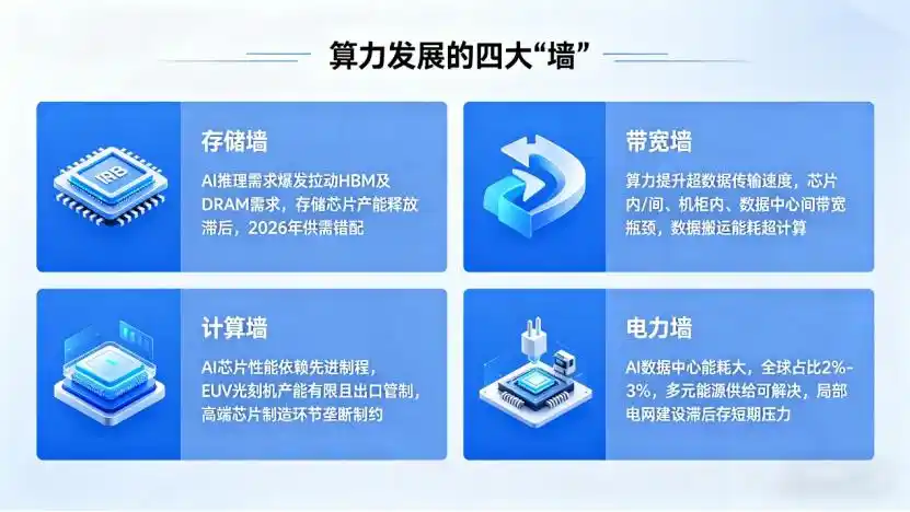
(1) Memory Wall: The First Shackle in the AI Inference Era
Currently, the AI industry is shifting its focus from large model training to inference, with global AI inference demand expected to surpass training scenarios by 2026. The explosion in AI inference demand directly drives the need for high-bandwidth memory (HBM) and high-capacity DRAM.
Although major memory chip manufacturers are planning to expand production capacity, it takes at least two years from investment to actual production line operation, meaning the supply shortage is unlikely to ease in the short term. New capacity is primarily set to come online in 2027 and beyond, leading to a structural mismatch in 2026 where demand grows rapidly while supply lags.
(2) Bandwidth Wall: The "Clogged Capillaries" of Data Flow
The speed of computing power improvement far exceeds that of data transmission. This contradiction has led to a severe "bandwidth wall" problem—data flow within chips, between chips, within server racks, and between data centers has become the performance bottleneck of the entire computing system.
The current bandwidth bottleneck is multi-layered: within chips, interconnect delays and power consumption between transistors are continuously rising; between chips, traditional PCB board interconnects can no longer meet the high-bandwidth, low-latency demands of AI chips; within server racks, interconnect bandwidth between servers has become a constraint for Scale Up (vertical scaling); between data centers, long-distance transmission bandwidth and latency limit the efficiency of Scale Out (horizontal scaling) and cross-regional computing power scheduling.
Estimates show that in current AI training clusters, the energy consumption of data movement already exceeds that of computation itself. How to unclog the "capillaries" of data flow and reduce transmission latency and power consumption is a critical issue that must be addressed for AI Infra development.
(3) Compute Wall: High-End Chip Manufacturing as the Fundamental Constraint
AI chip performance iteration heavily relies on advanced process technologies, and the production capacity of these advanced processes is entirely constrained by upstream high-end manufacturing equipment, particularly EUV (extreme Ultraviolet) lithography machines.
Currently, only ASML can produce EUV lithography machines globally, with extremely limited capacity and strict export controls. This directly results in a severe shortage of capacity for processes below 7nm, unable to meet the explosive demand for AI chips. As the global leader in AI chips, NVIDIA's delivery of high-end chips like the H100 and H200 has been constrained by TSMC's advanced process capacity, with lead times stretching to several months or even over a year.
More critically, chip manufacturing is a highly globalized industry chain; a break in any single link affects the entire production capacity. From raw materials like photoresists, target materials, and electronic special gases to key equipment like etching and deposition tools, there are varying degrees of monopoly and supply constraints. This makes high-end chip manufacturing capability the most challenging bottleneck to break through in the AI Infra industry chain.
(4) Power Wall: A Relatively Controllable Short-Term Challenge
Compared to the first three, the power wall is a relatively easier bottleneck to solve. AI data centers are major energy consumers; the annual electricity consumption of a single ultra-large data center campus can even exceed that of a medium-sized city with hundreds of thousands of people. Currently, global data center electricity consumption accounts for 2% to 3% of total global electricity use and is still climbing. But the power issue is essentially an infrastructure construction problem that can be addressed through diversified energy supply methods like gas turbines, fuel cells, and photovoltaics.
In the long run, with the development of renewable energy technologies and the improvement of energy infrastructure, power supply will not become the biggest mid-to-long-term bottleneck for AI computing power development. However, in some regions, short-term power supply pressures due to lagging grid construction may still limit the pace of data center construction.
The "Invisible Killer" of Capacity Expansion: Comprehensive Shortages in Equipment and Materials
The pace of AI chip capacity expansion is far slower than expected, with the core constraint not being the chips themselves but comprehensive shortages in upstream equipment and materials.
(1) Rapid Growth in Demand for Testing Equipment
AI chip technology upgrades are driving higher precision and efficiency requirements for testing equipment. Compared to ordinary logic chips, AI GPUs have a massive increase in signal ports, consuming more signal channel resources of testers; simultaneously, the surge in transistor count leads to a significant increase in corresponding test vector scale and per-chip testing time. More critically, while only a certain percentage of chips in traditional consumer electronics are tested, for AI chips, 100% of chips must be tested, often through multiple stages, to ensure the entire chipset operates normally. Driven strongly by AI computing demand and the memory market explosion, semiconductor test equipment (ATE) has become one of the fastest-growing categories in the semiconductor equipment sector.
Advantest, the world's largest chip test equipment supplier, also stated that it expects record highs for the fiscal year ending March 2026, with revenue projected to grow 37% and net profit more than doubling from the previous year.
(2) IC Substrates/Package Substrates: The "Choke Point" More Expensive Than Chips
Surprisingly, the biggest supply chain pain point for leading chip manufacturers like NVIDIA is not the chips themselves, but IC substrates (package substrates). IC substrates are key components connecting chips to PCB boards, providing electrical connection and physical support. AI chips have extremely high requirements for IC substrates—they need larger area, higher wiring density, better thermal performance, and lower signal loss. This also means their value is inevitably much higher than ordinary PCBs. Estimates show that IC substrates account for about 50% of the total packaging cost, and in advanced flip-chip packaging, this proportion can even reach 70%–80%. Depending on the resin material used, IC substrates are mainly divided into BT substrates and ABF substrates. BT substrates are primarily used for various memory chips, while ABF is more focused on logic chips like CPUs, GPUs, FPGAs, and ASICs.
According to incomplete statistics, since 2025, IC substrate prices have accumulated an increase of over 30%. The price hike is mainly due to two reasons: first, cost transmission from upstream raw materials—core materials like high-end glass fiber cloth and copper foil have been in continuous short supply since 2025, with the capacity gap不断扩大 (expanding); second, the explosion in demand for 2.5D/3D advanced packaging—high-end chips like GPUs普遍采用 (commonly adopt) multi-chip stacking architectures, and the significant increase in chip layers and area directly drives up the demand for substrate area.
Unlike ordinary PCBs, IC substrates have high technical barriers and complex processes. Global capacity for high-end IC substrates is mainly concentrated in a few Taiwanese manufacturers like Unimicron and Nan Ya PCB, with capacity expansion cycles as long as 18-24 months. This means the tight supply situation for IC substrates is unlikely to be fundamentally alleviated within the next two years.
(3) Key Specialty Materials: The Extremely Scarce "Industrial MSG"
Some seemingly insignificant specialty materials are becoming the "Achilles' heel" of the AI industry chain. Materials like Low-CTE (low coefficient of thermal expansion) glass fiber, specialty copper foil, and high-end drill bits, though used in small quantities, are indispensable "industrial MSG" for manufacturing high-end IC substrates and PCB boards.
The high power consumption and performance requirements of AI chips necessitate the use of materials with extremely low thermal expansion coefficients for substrates and PCBs to prevent deformation under high-temperature operating conditions. Simultaneously, as fillers are used, the lifespan of drill bits used in the加工过程 (processing) is drastically reduced to 1/5-1/7 of the original, leading to an explosive growth in demand for drill bits.
These specialty materials have extremely high technical barriers, global capacity is highly concentrated, and expansion is difficult. Any supply interruption will directly impact the normal operation of the entire AI industry chain.
(4) High-End Cleanrooms: The Overlooked High-Barrier Segment
In the AI industry chain's capacity expansion, high-end cleanrooms are another severely overlooked high-barrier segment. Advanced process chips and advanced packaging have extremely high requirements for production environment cleanliness—a single speck of dust in the air can cause an entire wafer to be scrapped.
The construction of high-end cleanrooms requires not only huge capital investment but also extremely high technical expertise. From air purification systems to anti-static facilities, from temperature and humidity control to vibration isolation, every环节 (aspect) has strict standards. Currently, the global high-end cleanroom market is mainly dominated by overseas companies, with net profit margins potentially exceeding 20%, far higher than domestic counterparts.
With the global expansion of AI chip capacity, demand for high-end cleanrooms remains strong, making it a segment with extremely strong certainty and high prosperity within the industry chain.
The "Route Dispute" in Connection Technology: Copper Resurgence and Photonic-Electronic Integration
Beyond computing and expansion bottlenecks, connection technology inside data centers is undergoing a profound transformation. The technological路线之争 (route dispute) between copper and light, along with the technological upgrades of PCB/substrates, is reshaping the connectivity landscape of AI Infra.
(1) Scenario-Based Competition and Substitution Between Copper and Light
For a long time, optical modules have been considered the future direction for high-speed interconnection in data centers. But with the explosion of AI computing demand, copper cable technology is experiencing a "resurgence," with copper and light forming a relationship of complementarity and substitution in different scenarios.
Short Distance (≤7 meters): Copper cables (AEC, Active Electrical Cables), with advantages of low cost, high reliability, and low latency, are comprehensively replacing laser-based optical modules. In short-distance interconnection scenarios within servers and within server racks, copper cables offer significant cost-performance advantages.
Medium Distance (~30 meters): Micro LED optical cables have become a compromise solution. They combine the advantages of copper cables and optical modules, offering better reliability than laser optical modules and lower cost than traditional optical modules, suitable for medium-distance interconnection between racks.
Long Distance (Between Data Centers): Traditional pluggable optical modules and fiber optics remain mainstream. CPO (Co-Packaged Optics) technology is considered the future direction; it integrates the optical engine with the chip package, significantly increasing bandwidth and reducing power consumption. However, it still faces challenges like high cost and poor reliability, and widespread commercial use is still some time away.
It is worth noting that the procurement scale and performance specifications for optical fiber in AI data centers have already created an order-of-magnitude difference compared to traditional telecom networks. To meet the low-latency, high-bandwidth interconnection needs of GPU clusters, demand for特种光纤 (specialty optical fibers) like G.657.A2 continues to rise, and more cutting-edge hollow-core fiber solutions have entered the deployment stage. Hollow-core fiber replaces the traditional glass core with air, significantly optimizing transmission: transmission loss can be reduced from the常规 (conventional) 0.14dB/km to below 0.1dB/km, transmission delay reduced from 5μs/km to 3.46μs/km, while tolerating higher optical power.
Currently, the number of participants in the hollow-core fiber market is expanding rapidly, but prices remain relatively stable, at about 30,000-40,000 RMB per kilometer, far higher than普通光纤 (ordinary optical fiber).
(2) Technological Upgrade Pressure on PCB/Substrates
To meet the high-bandwidth demands of AI chips, PCB and substrate technologies are also continuously upgrading. Currently, PCB/substrates are moving towards n+m layer structures, glass substrates, and modified Semi-Additive Process (mSAP) technology.
The n+m structure increases the number of layers and wiring density, enhancing the substrate's bandwidth capability; glass substrates have a lower coefficient of thermal expansion and better high-frequency performance, representing an important future direction for high-end substrates; mSAP technology enables finer circuit wiring, meeting high-density interconnection demands.
These technological upgrades place new demands (提出了全新的要求) on upstream equipment, materials, and manufacturing processes, also bringing new industrial opportunities and challenges.
Summary
The AI Infra industry chain is facing intertwined constraints from multiple bottlenecks. From the computing层面的 (level) memory wall, bandwidth wall, compute wall, and power wall, to expansion-level shortages in testing equipment, IC substrates, specialty materials, and cleanrooms, to the technological route dispute at the connection level, every环节 (link) affects the large-scale deployment of AI computing power.
High-end chip manufacturing capability is the most fundamental constraint, determining the performance上限 (upper limit) and production scale of AI chips. Testing equipment, high-end IC substrates, key specialty materials, etc., are currently the segments with the strongest certainty and the most acute supply-demand矛盾 (contradiction). In the long run, AI Infra development will show two major trends: first, the technological evolution of copper cable resurgence and photonic-electronic integration, where different technological routes will coexist in their respective advantageous scenarios; second, the restructuring of the global industry chain and the acceleration of localization, where domestic companies are expected to achieve breakthroughs in some细分领域 (segments).
This article is from the WeChat public account "Semiconductor Industry Vertical and Horizontal" (ID: ICViews), author: Peng Cheng