# Photonics İlgili Makaleler

HTX Haber Merkezi, kripto endüstrisindeki piyasa trendleri, proje güncellemeleri, teknoloji gelişmeleri ve düzenleyici politikaları kapsayan "Photonics" hakkında en son makaleleri ve derinlemesine analizleri sunmaktadır.

Three Industry Signals from the Systematic Revision of the 'Regulations on the Protection of Integrated Circuit Layout Designs'

The revised "Regulations on the Protection of Integrated Circuit Layout Designs" were promulgated on July 23, 2026, marking the first comprehensive amendment since its 2001 implementation. The revision sends three key industry signals. First, the protection scope is expanded from "semiconductor" to include "semiconductor + photonics + quantum," formally covering next-generation technologies like silicon photonics and quantum chips in the post-Moore era. Second, it introduces a "statement of originality" system to address long-standing difficulties in defining protection scope and proving infringement. Applicants must now clearly indicate the original portions of their design. Procedures for rejection, revocation (including third-party initiated), and rights restoration are also refined. Third, infringement penalties are significantly strengthened, shifting from compensatory to punitive damages. For willful and serious infringement, punitive damages of 1 to 5 times the actual loss, illicit profits, or license fees can be applied. Beneficiaries include IC design firms in emerging fields and IP suppliers. Entities facing new pressure include those reliant on reverse engineering, applicants filing fraudulent registrations, and packaging/test houses with heightened compliance duties. The amendment provides clearer rules, but their practical impact will be tested in post-implementation judicial practice, where courts are expected to strictly scrutinize rights foundations, originality, and commercial use timelines.

marsbit21 saat önce

Three Industry Signals from the Systematic Revision of the 'Regulations on the Protection of Integrated Circuit Layout Designs'

marsbit21 saat önce

The Domestic Answer to Space Computing Power: Photonics Are More Efficient, Musk and Huang's Approaches Are Too Roundabout

The Space Computing Race: A Photonic Advantage The competition for space-based computing has intensified, with figures like Elon Musk and NVIDIA's Jensen Huang highlighting its potential. Musk predicts solar-powered AI satellites could offer the most cost-effective computing by 2032. However, space presents extreme challenges for traditional electronic chips: radiation from cosmic particles can cause errors, the vacuum environment hinders heat dissipation, and limited solar power constrains energy-hungry systems. Photonic computing, using light instead of electrons, offers a promising solution. Its core advantages for space are threefold: 1) **Radiation Resistance**: Photons are charge-neutral, making them inherently immune to particle interference. 2) **Low Heat Generation**: Light propagation in waveguides generates minimal heat, bypassing critical thermal management issues. 3) **Low Power Consumption**: Photonic chips have near-zero static power draw, aligning perfectly with the energy constraints of satellites. Furthermore, for a given payload weight and volume, photonic systems can potentially deliver higher total compute density. Since they require less bulky cooling and power infrastructure, more space can be allocated to the compute units themselves. While photonic computing holds great promise, current industry approaches face hurdles like the memory-compute bottleneck (separate storage and processing) and challenges in large-scale integration. Engineering for space—withstanding launch vibrations and validating full system operation in orbit—remains a critical step. The path forward resembles the evolution from single GPUs to computing clusters, but via a photonic route. As electronic chips approach physical limits in miniaturization, photonic computing and optical interconnects (光算光联) may provide a key alternative to bypass these constraints and define the next generation of space-based computing capabilities.

marsbit06/28 04:31

The Domestic Answer to Space Computing Power: Photonics Are More Efficient, Musk and Huang's Approaches Are Too Roundabout

marsbit06/28 04:31

From the White-Haired Stock God to the Billion-Dollar Fund Titan: The Smart People Shorting NVIDIA Are Getting Rich Using the Same Framework

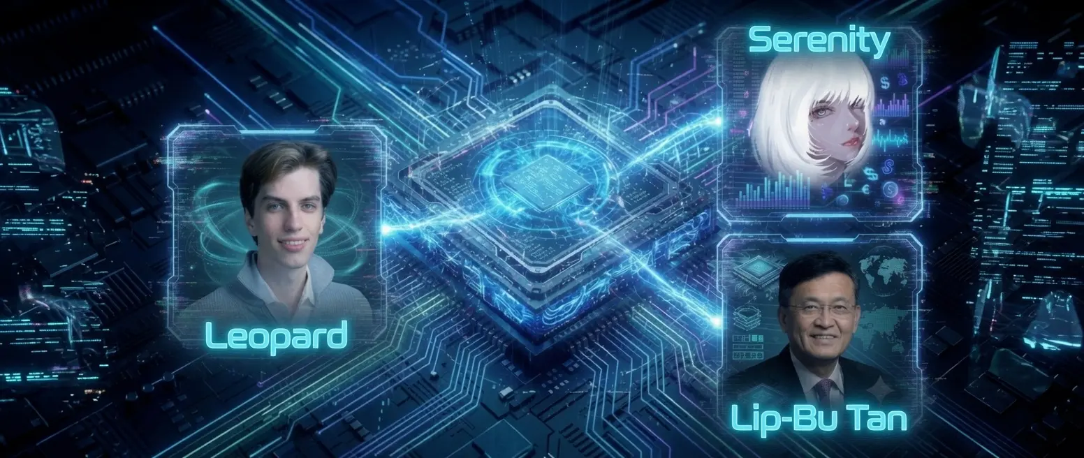
From "white-haired stock god" to billionaire fund manager, those profiting from shorting NVIDIA share a common framework. The article analyzes the critical bottlenecks in the AI hardware supply chain, which have become key investment focal points. The core argument is that the real constraint on the AI boom isn't software or algorithms, but fundamental physical infrastructure. The piece dissects nine major bottlenecks, organized around the lifecycle of an AI accelerator circuit board. *Before the Board*: The pre-manufacturing stage faces constraints in EDA tools, new materials (like GaN, SiC, InP) replacing silicon, and the critical, non-renewable supply of helium for semiconductor fabrication. *On the Board*: The primary bottlenecks are High-Bandwidth Memory (HBM), essential for unleashing GPU power, and advanced packaging (e.g., CoWoS), required to integrate components. Both are in severe shortage. *Between Boards*: Chip-to-chip communication is hitting limits with copper, pushing photonics and optical interconnects (CPO) as the next-gen solution, with NVIDIA heavily investing in this area. *Around the Board*: Power delivery requires new materials (GaN/SiC) for efficient voltage conversion from 48V to sub-1V. High-density AI racks (120kW+) are forcing a shift from air to liquid cooling as the standard. *Beyond the Board*: The ultimate bottleneck is electricity. AI data centers consume power equivalent to mid-sized cities, and grid expansion lags far behind demand, causing project delays and a scramble for power contracts. Prominent investors like Leopold and "white-haired stock god" are heavily betting on these infrastructure bottlenecks. Leopold's fund, for instance, holds no NVIDIA stock but uses massive put options to short the semiconductor sector while going long on power and physical infrastructure. His thesis is that while chip competition may eventually erode margins, the scarcity of foundational elements like electricity is more persistent. The framework's validity is tied to the supply-demand gap. Major new capacity in HBM and photonics is scheduled for 2027-2028, but demand continues to outpace it. Experts like Intel's CEO suggest no relief before 2028. However, the article warns of a potential reversal around 2028-2029 if AI capex slows and new capacity floods the market, turning scarcity into oversupply. Until then, the imbalance persists.

链捕手06/26 01:29

From the White-Haired Stock God to the Billion-Dollar Fund Titan: The Smart People Shorting NVIDIA Are Getting Rich Using the Same Framework

链捕手06/26 01:29

From Corning to Ciena: The 10x Opportunity in the AI Optical Communication Chain

The transition from copper to optical communication in AI data centers is creating significant investment opportunities beyond just chipmakers. The entire photonics supply chain, from glass and fiber to connectors and test equipment, is critical. Corning, a key fiber supplier, has locked in multi-billion dollar, multi-year contracts with major cloud providers (Meta, Amazon, Google, Microsoft, OpenAI, NVIDIA), demonstrating pricing power and scale. Its profit growth is outpacing revenue growth. In the interconnect layer, Amphenol benefits from high growth in AI data centers, driven by strategic acquisitions and operational efficiency, while Credo Technology acts as a bridge between copper and optical solutions, though with high customer concentration risk. At the systems level, Ciena enables higher data capacity on existing fiber lines, with a strong backlog and cloud customer adoption. Further upstream, AXT is a bottleneck supplier of key indium phosphide wafers for lasers but faces geopolitical supply chain risks. VEO Solutions provides essential testing equipment for the entire photonics industry. A new pure-play photonics ETF (FOTO) offers a consolidated investment approach. The core thesis is that the physical limits of copper are driving an inevitable shift to optical technologies, with wealth flowing to essential, often overlooked, suppliers across the photonics value chain.

marsbit06/24 07:14

From Corning to Ciena: The 10x Opportunity in the AI Optical Communication Chain

marsbit06/24 07:14

From Corning to Ciena: The 10X Stock Opportunities in the AI Optical Communication Chain

From Copper to Light: The AI-Driven Optical Communication Supply Chain and Investment Opportunities The exponential data demands of AI are pushing data centers beyond the physical limits of copper cables, forcing a critical transition to optical communication. This shift from electrical to photonic signals over distances greater than ~3 feet solves heat, power, and bandwidth constraints. The real investment opportunity lies not just in headline chipmakers, but across the entire essential photonics supply chain. **Key Investment Layers & Companies:** * **Glass & Fiber:** **Corning** is a dominant, irreplaceable supplier of advanced fiber to all major cloud/AI players (Meta, Amazon, Google, MSFT, OpenAI, NVIDIA), with multi-billion-dollar, multi-year contracts locked in years ahead of delivery. Its profit growth (93%) far outpaces revenue growth (36%), showing pricing power. * **Interconnects:** **Amphenol**, a consolidating giant in high-speed connectors (both copper and optical), shows robust growth (>80% in AI data centers) and expanding margins post-acquisition. **Credo Technology** bridges old and new worlds, extending copper's life in racks while moving into optics. It has hyper-growth but carries high customer concentration risk. * **Systems:** **Ciena** is a leader in coherent optics, enabling massive data capacity upgrades on existing fiber. It has a massive, growing order backlog ($~7B) and strong ties with cloud providers. * **Upstream & Enablers:** **AXT** produces mission-critical indium phosphide wafers for lasers, creating a supply bottleneck, but faces significant geopolitical/export license risk from its China-based manufacturing. **VEO Solutions** is the essential "picks and shovels" play, providing test equipment needed by every component in the optical chain, regardless of the eventual winner. A new pure-play photonics ETF (**FOTO**) offers a consolidated investment vehicle for this theme, though it is new and small. The core thesis is clear: the move from copper to light is inevitable and accelerating, with wealth creation spreading across this critical, multi-layered supply chain.

marsbit06/23 04:58
From Corning to Ciena: The 10X Stock Opportunities in the AI Optical Communication Chain

marsbit06/23 04:58

活动图片