τ Scaling: Huawei's New Growth Engine Designed for the Post-Moore Era

marsbitPublicado em 2026-05-25Última atualização em 2026-05-25

Resumo

**Tau Scaling: Huawei's New Growth Engine for the Post-Moore Era** For 60 years, progress in semiconductors was driven by Moore's Law – making transistors smaller, denser, and cheaper. This path has now stalled due to plummeting returns below 7nm, astronomical lithography costs, and rising per-transistor expenses. After six years and testing 381 production chips, Huawei’s semiconductor team proposes a fundamental shift: **stop competing on size, start competing on time**. This is the core of their "τ (Tau) Scaling" theory. It treats *time* as the key optimization metric, compressing characteristic delays (τ) across all levels – from transistor switching (picoseconds) to data center tasks (seconds), spanning 12 orders of magnitude. **What is τ Scaling?** It holistically minimizes delay/time constants (τ) across four layers: transistors (switching speed), circuits (signal delay), chips (compute/memory access), and systems (end-to-end communication). The goal is to align optimization from process and circuit design to architecture and systems using this unified metric. **Mobile Application: LogicFolding** Without advancing the process node, this technique vertically stacks chips using ultra-precision hybrid bonding, distributing critical paths across layers ("stacking floors"). Results include a 55% transistor density increase, 41% better energy efficiency, over 40% higher SRAM frequency, and a roadmap targeting 4GHz by 2029. **AI Data Center Application: Full-Link Latency ...

For the past 60 years, the semiconductor industry has been driven by shrinking transistor sizes (Moore's Law) for progress—making them smaller, denser, and cheaper.

But now this path is stalling:

  • Benefits of processes below 7nm plummet
  • Lithography machine costs are astronomical
  • Design cost for a single advanced-node chip exceeds $10 billion
  • Cost per transistor is no longer falling, but rising

Huawei's semiconductor team, after 6 years and verification across 381 mass-produced chips, has identified a new direction:

Stop competing on size, start competing on time.

They propose the τ Scaling theory (τ Scaling):

Treat "time" as the core optimization metric, compressing the characteristic time τ across the entire technology chain—from transistor switching (picoseconds) to data center tasks (seconds), covering 12 orders of magnitude.

Simply put:

It used to be about who is smaller; now it's about who is faster, has lower latency, and higher efficiency.

1. What Exactly is τ Scaling?

τ represents the delay/time constant at each layer, divided into four levels:

  • Transistor: Switching speed
  • Circuit: Signal transmission delay
  • Chip: Computation and memory access latency
  • System: End-to-end communication and synchronization time

The goal is to compress τ stack-wide. Process, circuits, architecture, and systems are optimized using the same set of metrics, ending siloed optimization.

2. Mobile Implementation: LogicFolding

Without advancing the process node, chips are stacked vertically. Ultra-precise hybrid bonding splits critical paths across multiple layers, essentially "adding floors" to the chip.

  • Transistor density: Increased by 55% in one generation, from 155→238 million/mm²
  • Energy efficiency: Improved by 41%, with main frequency rising nearly 13%
  • SRAM frequency: Increased by over 40%
  • Kirin 2026 target: 3.1GHz main frequency, aiming for 4GHz by 2029

3. AI Data Center Implementation: End-to-End Latency Reduction

In AI clusters, 80% of energy consumption and 70% of cost come from data movement. The core is reducing communication time.

1. Unified Bus

Removes multi-layer protocols, slashing remote access latency from tens of microseconds to about 100 nanoseconds—500 times faster.

2. Hi-ONE Optical Interconnect

Single module achieves 8Tb/s. Replaces copper with fiber optics, extending distance from 1 meter to 100 meters, suitable for 10,000-card clusters.

3. 3D Folding

Solves the problem of "area scaling outpacing I/O scaling" in 2.5D packaging. Moves memory, power delivery, and optical interfaces to vertical layers, scaling them in sync with computing power.

  • Prediction: AI hardware integration density to increase over 100x by 2035

4. Logic and Memory Re-integration

CPUs and memory developed separately in the past. In the AI era, where data movement is more critical than computation, memory and logic must be tightly 3D integrated. Industry influence is shifting towards memory and packaging.

5. Remaining Challenges

  • EDA tools need to adapt to 3D stacking design
  • Optimization needed for wafer-to-wafer process variations and vertical interconnect loss
  • New standards for energy efficiency and benchmarks required

Conclusion

The size-centric era of Moore's Law is over; the era of time scaling has begun.

Without fixating on cutting-edge lithography machines, continuous improvements in performance and energy efficiency are still achievable through 3D stacking, system architecture, and interconnect optimization.

This will be the core trajectory for semiconductors in the next decade.

Criptomoedas em alta

Perguntas relacionadas

QWhat is the core concept of τ Scaling proposed by Huawei?

Aτ Scaling shifts the optimization focus from transistor size to time (τ) as the key metric. It aims to compress the characteristic time τ across the entire technology stack, from transistor switching speeds to system-level task latencies, to achieve faster performance, lower latency, and higher efficiency.

QHow does LogicFolding, as an application of τ Scaling in mobile chips, improve performance?

ALogicFolding vertically stacks chips using ultra-precise hybrid bonding to distribute critical paths across multiple layers. Without upgrading the manufacturing process, it increases transistor density by 55% (e.g., from 155 to 238 million/mm²), boosts energy efficiency by 41%, raises the main frequency by nearly 13%, and increases SRAM frequency by over 40%.

QWhat are the key technological implementations for reducing latency in AI data centers according to the τ Scaling approach?

AThe key implementations are: 1) Unified Bus, which reduces remote access latency from tens of microseconds to about 100 nanoseconds; 2) Hi-ONE optical interconnects, offering 8 Tb/s per module and extending reach from 1 meter to 100 meters; and 3) 3D Folding, which vertically integrates components like memory and power to scale with computing power and avoid 2.5D packaging bottlenecks.

QWhy does the article argue that the semiconductor industry is shifting focus from scaling size to optimizing time?

ABecause traditional scaling (Moore's Law) has become unsustainable: benefits plummet below 7nm, lithography costs are exorbitant, chip design fees exceed $1 billion, and the cost per transistor is rising instead of falling. Therefore, the new paradigm is to compete on speed, latency, and efficiency by optimizing the time factor τ across all levels.

QWhat are some of the remaining challenges for implementing the τ Scaling strategy mentioned in the article?

AChallenges include: adapting EDA tools for 3D stacked design; optimizing process variations between wafers and losses in vertical interconnects; and establishing new standards for energy efficiency and benchmarking to support this new approach.

Leituras Relacionadas

Stocks of Companies in Bitcoin Mining and AI Infrastructure Soar, Short Sellers Face Losses

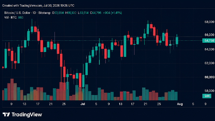
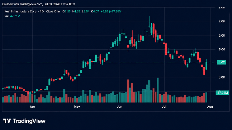
Shares of companies involved in Bitcoin mining and AI infrastructure surged, causing losses for short sellers. On Thursday, July 30, 2026, Keel Infrastructure (formerly Bitfarms) led the gains, rising 29.13%, followed by Nebius Group, Cipher Digital, and IREN Limited with jumps over 27%. Other notable gainers included Riot Platforms, Bitdeer, Core Scientific, Hut 8, and Cleanspark, with increases mostly ranging from 17% to 24%. The rally was attributed to a short squeeze triggered by a hedge fund's forced liquidation of its holdings, which were largely bought by Citadel. Additionally, Bitcoin trading above $64,000 and strong Microsoft earnings, highlighting AI's profitability, boosted market sentiment. Coreweave also announced a deal to provide AI cloud services for U.S. defense and intelligence agencies. This surge reflects a broader, longer-term trend of Bitcoin miners pivoting to AI data centers, leveraging their existing energy infrastructure and land. Recent multi-billion dollar deals by companies like Hut 8, IREN, and Terawulf for AI cloud services underscore this strategic shift. Other gainers, including Sandisk, Micron, Bloom Energy, and Cerebras, are suppliers critical to the AI infrastructure build-out. While the rally provided relief after July's losses, questions remain about capital expenditures, power availability, and long-term AI demand. The sustainability of these gains depends on these companies successfully converting their energy contracts and AI service deals into stable revenue streams.

cryptonews.ruHá 6m

Stocks of Companies in Bitcoin Mining and AI Infrastructure Soar, Short Sellers Face Losses

cryptonews.ruHá 6m

Trading

Spot

Artigos em Destaque

Como comprar ERA

Bem-vindo à HTX.com!Tornámos a compra de Caldera (ERA) simples e conveniente.Segue o nosso guia passo a passo para iniciar a tua jornada no mundo das criptos.Passo 1: cria a tua conta HTXUtiliza o teu e-mail ou número de telefone para te inscreveres numa conta gratuita na HTX.Desfruta de um processo de inscrição sem complicações e desbloqueia todas as funcionalidades.Obter a minha contaPasso 2: vai para Comprar Cripto e escolhe o teu método de pagamentoCartão de crédito/débito: usa o teu visa ou mastercard para comprar Caldera (ERA) instantaneamente.Saldo: usa os fundos da tua conta HTX para transacionar sem problemas.Terceiros: adicionamos métodos de pagamento populares, como Google Pay e Apple Pay, para aumentar a conveniência.P2P: transaciona diretamente com outros utilizadores na HTX.Mercado de balcão (OTC): oferecemos serviços personalizados e taxas de câmbio competitivas para os traders.Passo 3: armazena teu Caldera (ERA)Depois de comprar o teu Caldera (ERA), armazena-o na tua conta HTX.Alternativamente, podes enviá-lo para outro lugar através de transferência blockchain ou usá-lo para transacionar outras criptomoedas.Passo 4: transaciona Caldera (ERA)Transaciona facilmente Caldera (ERA) no mercado à vista da HTX.Acede simplesmente à tua conta, seleciona o teu par de trading, executa as tuas transações e monitoriza em tempo real.Oferecemos uma experiência de fácil utilização tanto para principiantes como para traders experientes.

536 Visualizações TotaisPublicado em {updateTime}Atualizado em 2026.06.02

Como comprar ERA

Discussões

Bem-vindo à Comunidade HTX. Aqui, pode manter-se informado sobre os mais recentes desenvolvimentos da plataforma e obter acesso a análises profissionais de mercado. As opiniões dos utilizadores sobre o preço de ERA (ERA) são apresentadas abaixo.

活动图片