# Huawei İlgili Makaleler

HTX Haber Merkezi, kripto endüstrisindeki piyasa trendleri, proje güncellemeleri, teknoloji gelişmeleri ve düzenleyici politikaları kapsayan "Huawei" hakkında en son makaleleri ve derinlemesine analizleri sunmaktadır.

Former Huawei 'Genius Teen' Who Questioned DeepSeek Interview Lands in 'Crossfire' from Web3 Investor

Former Huawei "Genius Youth" Li Bojie recently drew public attention by criticizing his interview experience with DeepSeek. The controversy escalated when Du Jun, co-founder of Web3 investment firm ABCDE Capital, publicly accused Li of being "the founder with the least sense of contractual spirit" he had ever cooperated with, sparking a dispute over Li's startup project, Metagent. Li detailed a frustrating DeepSeek interview where he was accused of potential plagiarism, leading him to end the session. The spotlight then shifted to his venture, Metagent, a Web3+AI project aiming to tokenize AI agents. ABCDE invested $1.5 million, with an initial $500k disbursed. Du Jun claimed the project's progress was severely lacking, with a poor-quality demo and minimal social media activity. He alleged Li stopped communicating, deleted his Telegram, and failed to provide proper financial reporting. In response, Li argued the remaining $1 million was never received, crippling operations and forcing salary cuts. He stated he left Metagent in October 2024 due to family reasons and Web3 compliance concerns, with board approval. He claimed to have fulfilled disclosure duties and that his subsequent projects avoided conflicting fields. Other investors, including ArkStream Capital, shared negative due diligence experiences, citing unprofessional contracts and evasive answers on tokenomics. Metagent's social media went silent in June 2024, effectively stalling. Li has since moved to a new consumer AI agent platform, Pine AI (formerly Logenic AI), which has raised $25 million in Series A funding. He served as its Chief Scientist but recently left, clarifying he was not the founder and departed due to a shift in research interests.

Foresight News07/08 09:40

Former Huawei 'Genius Teen' Who Questioned DeepSeek Interview Lands in 'Crossfire' from Web3 Investor

Foresight News07/08 09:40

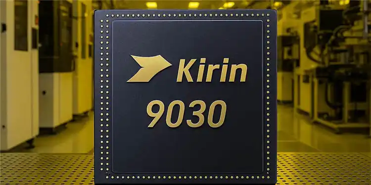
SemiAnalysis Dissects Huawei's Kirin 9030: Process Technology Halted, So They Folded the Chip

SemiAnalysis has published a detailed teardown report on the HiSilicon Kirin 9030 Pro chipset found in Huawei's Mate 80 Pro. Fabricated using SMIC's most advanced N+3 node without EUV lithography, the analysis reveals significant technical achievements and strategic shifts. The report indicates SMIC's N+3 has achieved transistor density comparable to TSMC's N6 (113.4 vs 107.7 MTr/mm²), primarily through aggressive use of Self-Aligned Quadruple Patterning (SAQP) for its metal layers. This results in a notably small 32.5nm M0 metal pitch. However, SemiAnalysis notes this achievement comes with significantly higher process complexity, cost, and potential yield challenges compared to competitors using more advanced tools. The Kirin 9030 design maximizes this constrained density. While its GPU performance has improved ~70% and matches Qualcomm's 2022 flagship level, the CPU core's IPC lags behind current top-tier designs from Apple and Qualcomm, a gap attributed to the underlying manufacturing technology rather than design capability. Facing long-term restrictions on advanced tools, Huawei is charting a new path. The report highlights the company's "LogicFolding" roadmap, a 3D stacking technique aimed at shortening signal paths to boost performance and efficiency. The goal is to reach 5GHz frequency and a projected density of 295 MTr/mm² by 2031. SemiAnalysis concludes that export controls have not halted China's chip progress but have fundamentally altered its trajectory, making it more expensive and complex. This has spurred innovation in alternative areas like 3D stacking and domestic EDA tool development, with Huawei's supply chain also beginning to integrate Chinese memory from CXMT.

marsbit06/15 06:52

SemiAnalysis Dissects Huawei's Kirin 9030: Process Technology Halted, So They Folded the Chip

marsbit06/15 06:52

Huawei's "Tao Law": A Comprehensive Overview of Core Companies

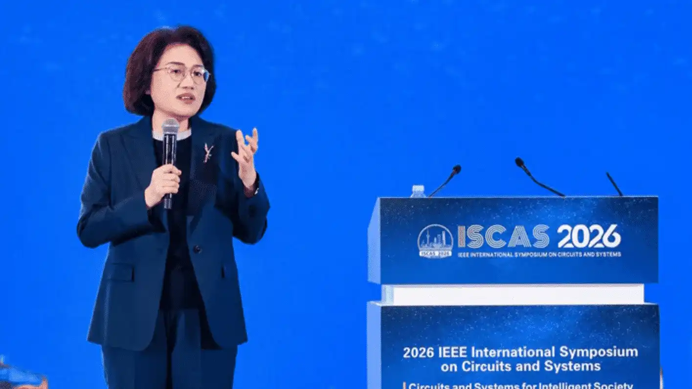
Huawei's "Tau Law": Core Companies Overview On May 25, 2026, Huawei's Director and President of the Semiconductor Business Division, He Tingbo, formally introduced the "Tau (τ) Law" at ISCAS 2026, marking a significant principle guiding industry development in the global semiconductor field from China. The Tau Law shifts focus from traditional Moore's Law, which pursues geometric transistor scaling, to "time scaling"—continuously compressing signal propagation delay (time constant τ) without solely relying on extreme feature size reduction. The core implementation path is "logic folding." This technique transforms circuit layouts from two-dimensional planes to multi-layer 3D stacks, using short vertical interconnects to replace long horizontal wiring, thereby drastically reducing τ. Huawei has already designed and mass-produced 381 chips following this principle over the past six years, with plans to launch a Kirin chip utilizing logic folding in Fall 2026. By 2031, high-end chips based on the Tau Law are expected to achieve performance levels equivalent to a 1.4nm process node. This development impacts several key industry segments, with related Chinese companies poised to benefit: 1. **EDA Design Software**: Essential for circuit-level optimization. Key players include: * **Empyrean Technology** (Huada Jiutian): China's largest full-flow EDA provider. * **Primarius Technologies** (Gailun Dianzi): Specializes in device modeling and verification. * **Semitronix** (Guangliwei): Focuses on yield enhancement and test chip EDA. 2. **Chiplet & Advanced Packaging**: Logic folding's 3D stacking necessitates advanced packaging (e.g., TSV, hybrid bonding). Core participants are: * **Tongfu Microelectronics**: A leader in advanced packaging and a key partner for AMD's Chiplet products. * **JCET Group** (Changdian Keji) & **Tianshui Huatian Technology**: Major OSATs with advanced packaging capabilities. * **VeriSilicon** (Xinyuan Gufen): Provides Chiplet-based design platforms and IP. 3. **Foundry Manufacturing**: Optimization must be implemented in transistor structures and process parameters. Potential foundries for Huawei's future chips include: * **SMIC**: China's leading foundry with advanced FinFET capabilities, the most likely candidate for next-gen Kirin chips. * **Hua Hong Semiconductor** (Huahong Gongsi): A leader in specialty processes (power, embedded memory). * **Nexchip Semiconductor** (Jinghe Jicheng): Major foundry for display driver ICs and MCUs. The Tau Law represents a strategic move towards architectural innovation and design-process co-optimization, driving demand across the domestic semiconductor supply chain.

marsbit05/25 11:33

Huawei's "Tao Law": A Comprehensive Overview of Core Companies

marsbit05/25 11:33

TechFlow Intelligence Report: Huawei Unveils "Tao" Law, Semiconductor Sector Surges; Meta Cuts 10% of Workforce

"TechFlow Intelligence Brief": Huawei's new "Tau Law" in semiconductors and Meta's 10% layoffs headline today's tech landscape. In AI, breakthroughs include an AI solving 9 high-difficulty pure math problems for just a few hundred dollars each, and DeepSeek's new Reasonix programming agent challenging commercial models. However, research highlights a "constraint decay" issue in LLM-generated backend code. Open-source model Qwen 3.6 27B achieves high speeds on older GPUs, sparking debate on NVIDIA's future dominance. In Crypto/Web3, Ethereum Foundation plans to downsize, possibly reducing ETH selling pressure. Fake news about CZ ignited a meme coin frenzy, showing the market's sensitivity to celebrity narratives. DeFi sees a new trend in HELOC-backed Real World Asset (RWA) pools. The chip sector is stirred by Huawei's proposed "Tau (τ) Law," aiming for 1.4nm-equivalent performance by 2031 through architectural innovation, causing related stocks to surge. A report notes memory now constitutes nearly two-thirds of AI chip cost. Meanwhile, executives at 7 Chinese semiconductor firms sold shares after price peaks. Meta announces 10% layoffs as it pivots to AI. Google's CEO faced student protests over AI ethics during a speech, and the company controversially published a Chromium exploit before patching was complete. Xiaomi permanently banned installers for AC installation fraud. In US stocks, AMD is seen as a potential challenger to NVIDIA, while a survey reveals 99% of CEOs expect AI-driven layoffs within two years. Palantir secured a government contract for employee monitoring, raising privacy concerns. Macro developments include a 6% drop in WTI crude oil on hopes for reopened Hormuz Strait, and silver prices rising over 4%. Global oil inventories are nearing critical lows. New trends highlight a "audio prompt injection" attack targeting AI voice assistants via hidden commands, and CBS pausing takedowns of pirated Stephen Colbert episodes after public pushback. The underlying narrative connects AI's cost-effective problem-solving, widespread planned job displacement, and Huawei's challenge to Western tech hegemony, framing the AI and chip race as a broader contest over employment, geopolitics, and the very definition of intelligence.

marsbit05/25 10:50

TechFlow Intelligence Report: Huawei Unveils "Tao" Law, Semiconductor Sector Surges; Meta Cuts 10% of Workforce

marsbit05/25 10:50

τ Scaling: Huawei's New Growth Engine Designed for the Post-Moore Era

**Tau Scaling: Huawei's New Growth Engine for the Post-Moore Era** For 60 years, progress in semiconductors was driven by Moore's Law – making transistors smaller, denser, and cheaper. This path has now stalled due to plummeting returns below 7nm, astronomical lithography costs, and rising per-transistor expenses. After six years and testing 381 production chips, Huawei’s semiconductor team proposes a fundamental shift: **stop competing on size, start competing on time**. This is the core of their "τ (Tau) Scaling" theory. It treats *time* as the key optimization metric, compressing characteristic delays (τ) across all levels – from transistor switching (picoseconds) to data center tasks (seconds), spanning 12 orders of magnitude. **What is τ Scaling?** It holistically minimizes delay/time constants (τ) across four layers: transistors (switching speed), circuits (signal delay), chips (compute/memory access), and systems (end-to-end communication). The goal is to align optimization from process and circuit design to architecture and systems using this unified metric. **Mobile Application: LogicFolding** Without advancing the process node, this technique vertically stacks chips using ultra-precision hybrid bonding, distributing critical paths across layers ("stacking floors"). Results include a 55% transistor density increase, 41% better energy efficiency, over 40% higher SRAM frequency, and a roadmap targeting 4GHz by 2029. **AI Data Center Application: Full-Link Latency Compression** With 80% of AI cluster energy and 70% cost spent on data movement, the focus is slashing communication time. Key innovations include: 1. **Unified Bus:** Cuts multi-layer protocols, reducing remote access latency from microseconds to ~100 nanoseconds – 500x faster. 2. **Hi-ONE Optical Interconnect:** Replaces copper with fiber, enabling 8Tb/s per module and scaling distances from 1m to 100m for 10,000-chip clusters. 3. **3D Folding:** Solves the "interface bottleneck" of 2.5D packaging by vertically integrating memory, power, and optical I/O alongside compute, predicting over 100x integration density gain by 2035. **Re-fusion of Logic and Memory** The AI era, where data movement is more critical than computation, demands tight 3D integration of logic and memory, shifting industry influence towards memory and advanced packaging. **Remaining Challenges** include adapting EDA tools for 3D design, optimizing wafer-to-wafer process variation and vertical interconnect losses, and establishing new energy efficiency and benchmarking standards. **Conclusion:** The era of scaling physical dimensions is over. The era of scaling time has begun. By leveraging 3D stacking, system architecture, and interconnect optimization—rather than solely chasing advanced lithography—performance and efficiency can continue to advance. This is poised to be the semiconductor industry's core roadmap for the next decade.

marsbit05/25 05:35

τ Scaling: Huawei's New Growth Engine Designed for the Post-Moore Era

marsbit05/25 05:35

Autonomy or Compatibility: The Choice Facing China's AI Ecosystem Behind the Delay of DeepSeek V4

DeepSeek V4's repeated delay in early 2026 has sparked global discussions on "de-CUDA-ization" in AI. The highly anticipated trillion-parameter open-source model is undergoing deep adaptation to Huawei’s Ascend chips using the CANN framework, representing China’s first systematic attempt to run a core AI model outside the CUDA ecosystem. This shift, however, comes with significant engineering challenges. While the model uses a MoE architecture to reduce computational load, it places extreme demands on memory bandwidth, chip interconnects, and system scheduling—areas where NVIDIA’s mature CUDA ecosystem currently excels. Migrating to Ascend introduces complexities in hardware topology, communication latency, and software optimization due to CANN’s relative immaturity compared to CUDA. The move highlights a broader strategic dilemma: short-term compatibility with CUDA offers practical benefits and faster adoption, as seen in CANN’s efforts to emulate CUDA interfaces. Yet, long-term over-reliance on compatibility risks inheriting CUDA’s limitations and stifling native innovation. If global AI shifts away from transformer-based architectures, strict compatibility could lead to technological obsolescence. Despite these challenges, DeepSeek V4’s eventual release could demonstrate the viability of a full domestic AI stack and accelerate CANN’s ecosystem growth. However, true technological independence will require building an original software-hardware paradigm beyond compatibility—a critical task for China’s AI ambitions in the next 3-5 years.

marsbit04/21 10:16

Autonomy or Compatibility: The Choice Facing China's AI Ecosystem Behind the Delay of DeepSeek V4

marsbit04/21 10:16

The DeepSeek You've Been Waiting For Has Long Changed

The article discusses the delayed release of DeepSeek V4, a highly anticipated AI model in China, and explores the reasons behind its slowed development. Initially a leader in the global AI race, DeepSeek has fallen behind competitors like OpenAI, Anthropic, and Google, which release major updates every few months. A key factor is DeepSeek's shift in focus due to national strategic priorities. In early 2025, the Chinese government encouraged the company to use Huawei’s Ascend processors instead of NVIDIA’s GPUs, aligning with broader efforts to achieve technological self-reliance. DeepSeek attempted to train its models on Huawei’s Ascend 910C chips but faced technical challenges, including instability and communication issues during distributed training. As a result, the company continued using NVIDIA hardware for training while only using Ascend chips for inference. In 2026, DeepSeek prioritized adapting V4 to Huawei’s new Ascend 950PR and Cambricon chips, aiming for a full migration from NVIDIA’s CUDA to Huawei’s CANN framework. This adaptation process, particularly ensuring precision alignment across hardware, consumed significant time and resources, slowing down model iteration. The delay also reflects DeepSeek’s evolving role from a purely market-driven entity to a "national mission-oriented" company. This shift has come at a cost: the model now lags behind competitors in areas like code generation and multimodal capabilities, and the company has faced talent drain, with key researchers leaving for better-paying opportunities at larger tech firms. Despite these challenges, V4’s release is seen as a potential milestone for China’s AI industry, demonstrating that advanced models can run on domestic hardware ecosystems. While it may not be a groundbreaking model in terms of performance, its success could validate China’s broader strategy for AI independence.

marsbit04/15 10:32

The DeepSeek You've Been Waiting For Has Long Changed

marsbit04/15 10:32

NVIDIA's Market Share in China Drops Below 60%, Domestic AI Chips Seize Market with 1.65 Million Units Delivered Annually

Nvidia's market share in China's AI accelerator card market has declined significantly, dropping from approximately 95% to 55% in 2025, according to IDC data. During the same period, domestic Chinese manufacturers collectively captured 41% of the market, shipping 1.65 million units out of a total market of 4 million units. Huawei led the domestic suppliers with 812,000 units shipped, representing nearly half of the local market share. This shift is driven by both U.S. export controls and China’s aggressive domestic substitution policies. In November 2025, Beijing mandated that state-funded data centers must use domestic AI chips, accelerating the adoption of local alternatives. Huawei recently launched the Atlas 350 accelerator card, claiming 2.87 times the inference performance of Nvidia’s H20 in low-precision computing, though direct comparisons are complicated by architectural differences. While Chinese chips still lag behind in training large-scale AI models—estimated to be 5-10 years behind Nvidia—they have reached a "good enough" level for many commercial applications like inference tasks. The main challenge remains software ecosystem development, as Nvidia’s CUDA platform remains the industry standard. Chinese firms are responding with compatibility efforts and open-source initiatives. Several domestic AI chip companies are now pursuing IPOs, and Huawei continues heavy R&D spending to reduce foreign dependency. Even if U.S. export policies ease, the structural move toward domestic AI chips appears irreversible.

marsbit04/03 05:51

NVIDIA's Market Share in China Drops Below 60%, Domestic AI Chips Seize Market with 1.65 Million Units Delivered Annually

marsbit04/03 05:51

活动图片