# Optical Interconnect Articoli collegati

Il Centro Notizie HTX fornisce gli articoli più recenti e le analisi più approfondite su "Optical Interconnect", coprendo tendenze di mercato, aggiornamenti sui progetti, sviluppi tecnologici e politiche normative nel settore crypto.

"Shocking" CPO: How Does the Glass Bridge Actually Work? Detailed Explanation from Corning

Chinese CPO stocks plunged over 6% following Corning's announcement of its Glass Bridge platform at a Seoul tech conference. The new technology utilizes wafer-level glass ion-exchange waveguides for passive alignment between fibers and photonic chips, potentially simplifying traditional CPO architectures that rely on complex Fiber Array Units and active alignment equipment. This raised market concerns about reduced long-term demand for mid-stream CPO components. Corning's official documentation details Glass Bridge as a platform for fiber-to-PIC connectivity in NPO, CPO, and high-density modules. Its key features include wafer-level manufacturing for consistent, cost-effective production; a standardized, removable MT ferrule interface for ecosystem integration; and a separable high-density connector design supporting over 24 channels for assembly flexibility. Corning positions the technology as complementary to FAUs, addressing limitations in ultra-high-fiber-count scenarios. The market reaction reflects a broader reassessment of the AI optical interconnect value chain. Funds shifted from CPO and PCB manufacturing stocks towards glass substrate concept stocks like Kaisheng Technology and Dyer Laser. Analysts note glass substrates are seen as a next-gen advanced packaging material, offering a potential path for domestic industry differentiation amid AI-driven demand for high-performance, large-scale packaging, marking a structural migration in value towards upstream specialty materials.

marsbit06/28 10:41

"Shocking" CPO: How Does the Glass Bridge Actually Work? Detailed Explanation from Corning

marsbit06/28 10:41

The Domestic Answer to Space Computing Power: Photonics Are More Efficient, Musk and Huang's Approaches Are Too Roundabout

The Space Computing Race: A Photonic Advantage The competition for space-based computing has intensified, with figures like Elon Musk and NVIDIA's Jensen Huang highlighting its potential. Musk predicts solar-powered AI satellites could offer the most cost-effective computing by 2032. However, space presents extreme challenges for traditional electronic chips: radiation from cosmic particles can cause errors, the vacuum environment hinders heat dissipation, and limited solar power constrains energy-hungry systems. Photonic computing, using light instead of electrons, offers a promising solution. Its core advantages for space are threefold: 1) **Radiation Resistance**: Photons are charge-neutral, making them inherently immune to particle interference. 2) **Low Heat Generation**: Light propagation in waveguides generates minimal heat, bypassing critical thermal management issues. 3) **Low Power Consumption**: Photonic chips have near-zero static power draw, aligning perfectly with the energy constraints of satellites. Furthermore, for a given payload weight and volume, photonic systems can potentially deliver higher total compute density. Since they require less bulky cooling and power infrastructure, more space can be allocated to the compute units themselves. While photonic computing holds great promise, current industry approaches face hurdles like the memory-compute bottleneck (separate storage and processing) and challenges in large-scale integration. Engineering for space—withstanding launch vibrations and validating full system operation in orbit—remains a critical step. The path forward resembles the evolution from single GPUs to computing clusters, but via a photonic route. As electronic chips approach physical limits in miniaturization, photonic computing and optical interconnects (光算光联) may provide a key alternative to bypass these constraints and define the next generation of space-based computing capabilities.

marsbit06/28 04:31

The Domestic Answer to Space Computing Power: Photonics Are More Efficient, Musk and Huang's Approaches Are Too Roundabout

marsbit06/28 04:31

Optical Chips: Collective Capacity Expansion

The global optical chip industry is experiencing a massive wave of expansion driven by surging AI data center demand. Major players across the US, Japan, Europe, and China are aggressively investing to ramp up production capacity. In the US, Coherent is expanding its 6-inch Indium Phosphide (InP) semiconductor fab in Texas, supported by CHIPS Act funding and a $2 billion strategic investment from NVIDIA. Lumentum is building a new factory for InP optical devices, and Nokia is scaling its advanced photonic chip packaging and testing capabilities. NVIDIA's investments aim to secure future supply of critical lasers and optical interconnect products for AI infrastructure. Japan's JX Advanced Metals, a leading InP substrate supplier, plans a multi-billion yen investment to increase its capacity 7-10 times, strengthening its grip on the crucial upstream materials market. In Europe, IQE and Tower Semiconductor settled a patent dispute and signed a multi-year InP epitaxial wafer supply agreement, highlighting that next-generation silicon photonics platforms will integrate high-performance InP components. STMicroelectronics and Sivers Semiconductors are also expanding silicon photonics production and partnerships. China is rapidly building out its domestic supply chain. Dongshan Precision's subsidiary, Source Photonics, announced a $12 billion project to expand optical chip and module production. Companies like Sanan Optoelectronics and Yunnan Germanium are scaling up InP chip manufacturing and substrate production, moving towards vertical integration from materials to modules. While debate continues around the exact future architecture—whether CPO (Co-Packaged Optics), NPO, or pluggables will dominate—analysts like Morgan Stanley argue the underlying driver is unchangeable: the explosive growth in bandwidth demand. This will inevitably increase the volume of optical engines, lasers, and related content per GPU, regardless of the final technical path. The competition for "more light" in the AI era has intensified into a global, full-chain capacity race.

marsbit06/20 10:16

Optical Chips: Collective Capacity Expansion

marsbit06/20 10:16

Research Report Analysis: MRVL's Optical AI Booming, Why High Valuation Keeps Morgan Stanley's Star Analyst Sidelined?

Report Recap: MRVL Optical AI Boom - Why High Valuation Led Morgan Stanley's Star Analyst to Stay Neutral? Morgan Stanley analyst Joseph Moore maintained an "Equal-weight" (Neutral) rating on Marvell Technology (MRVL) on May 28, raising the price target from $172 to $195, below the trading price. This stance comes despite Marvell reporting a record quarter and significantly raising its full-year outlook (FY27 revenue ~$11.5B, up ~40%). Moore's neutral view is based on valuation. The $195 target implies ~40x CY2027 P/E. He contrasts MRVL with NVDA: both trade near ~$200, but Nvidia's forward EPS is more than double Marvell's. For MRVL's valuation to hold, it needs consistent earnings upgrades, proof of networking market share gains, or certainty on large-scale custom AI chip shipments—none of which are confirmed yet. Growth is driven by two pillars: **1) Optical Interconnect** (the faster runner): Moore raised FY27 growth expectations to >70%, with the optical module product line nearing a $1B annualized run rate. **2) Custom AI Chips** (the climber): Confidence in FY28 is growing, but a major new customer project only ramps in FY28, with no current revenue visibility. Key risks are the underperforming Storage, Enterprise, and legacy Networking segments. Moore acknowledges the real AI opportunity but believes the current price already reflects it. For the stock to work from here, investors need to see the optical business hit its targets, custom chips ramp as planned, and a recovery in the weaker business units.

marsbit06/17 11:39

Research Report Analysis: MRVL's Optical AI Booming, Why High Valuation Keeps Morgan Stanley's Star Analyst Sidelined?

marsbit06/17 11:39

Ten-Thousand-Word Analysis: From $10 to $290, MRVL Wins the Entire AI Era by 'Not Making GPUs'

Marvell Technology's stock price surged from under $10 in 2016 to a record $290 in June 2026, fueled not by making GPUs, but by dominating AI infrastructure connectivity. This analysis argues the market misvalues MRVL as merely a smaller Broadcom in custom AI chips, overlooking its true, unique position. Marvell's core strength lies in enabling high-speed data flow for AI clusters through three interconnected businesses. First, it holds a commanding ~70% market share in high-speed optical DSPs (essential for data center light modules), a deep-moat business with accelerating growth. Second, its custom AI chip design business serves hyperscalers like AWS, Microsoft, and Google, with a significant revenue pipeline despite lower margins. Third, stable cash flows come from Ethernet switch chips and enterprise storage controllers. Together, they form a full-stack "AI data movement" platform. CEO Matt Murphy's transformative leadership since 2016, involving strategic divestments, key acquisitions (like Inphi for optical DSPs), and securing long-term agreements with major cloud providers, repositioned the company. A pivotal $2 billion strategic investment from NVIDIA in 2026 underscored Marvell's critical role in the AI ecosystem, particularly through collaborations like NVLink Fusion. While Marvell faces risks—including client concentration (losing the Amazon Trainium3 design), lower-margin business mix, competitive threats, insider selling, and complex supply chains—its fundamentals remain strong. The optical interconnect moat is widening with the acquisition of Celestial AI (photonics fabric), and financial metrics show accelerating revenue growth and operating leverage. With a PEG ratio suggesting undervaluation relative to its growth, the thesis is that the market undervalues Marvell's monopolistic position in AI "plumbing" while overemphasizing its competitive custom chip segment. The story transcends investing, symbolizing how in any complex system—from the internet to AI—the value of "connection" ultimately surpasses that of individual "nodes."

marsbit06/04 06:40

Ten-Thousand-Word Analysis: From $10 to $290, MRVL Wins the Entire AI Era by 'Not Making GPUs'

marsbit06/04 06:40

Deconstructing the Investment Methodology of the 'Stock God Serenity' in One Article

"Serenity's Bottleneck Investment Methodology: A Deep Dive" This article dissects the "bottleneck point investment" strategy of the pseudonymous investor Serenity, known for exceptional returns (YTD 4502.45%). The core methodology involves identifying a major technological trend (e.g., AI compute expansion), mapping its supply chain, and investing early in the most irreplaceable, supply-constrained upstream component before the market fully values it. The framework is broken down into a five-factor model: 1. **Deterministic Demand**: Anchored in a large, validated trend. 2. **Constrained Supply**: The component must be difficult to replicate or scale quickly. 3. **Low Market Attention**: Opportunities exist where coverage is sparse. 4. **Value Capture**: The company must have pricing power, high margins, and customer lock-in. 5. **Catalyst**: A near-term event to trigger price discovery (earnings, customer ramp, etc.). The article provides illustrative examples like $AXTI (InP substrates for photonics), $RPI (edge hardware for AI agents), and $AAOI/$LITE (components for cloud ASICs). To apply this method, a six-step process is outlined: identify the macro trend, map the supply chain, pinpoint the true bottleneck, gather evidence (client wins, certifications), assess risks ("anti-thesis table"), and size the position according to research depth. Crucially, the article notes significant limitations: risk of overfitting inferences from sparse data, valuation challenges for pre-revenue companies, liquidity/reflexivity risks due to Serenity's own market influence, and survivor bias amplified by a strong AI bull market. The key takeaway is to emulate the rigorous research process—finding the trend, the bottleneck, the evidence—rather than blindly copying specific stock picks, emphasizing the discipline of "walking through the narrow gate."

marsbit05/30 06:45

Deconstructing the Investment Methodology of the 'Stock God Serenity' in One Article

marsbit05/30 06:45

One Article Deconstructs the Investment Methodology of 'Stock God Serenity'

This article deconstructs the "bottleneck point" investment methodology of the renowned investor known as "Serenity" (aleabitoreddit). Characterized by a YTD return of over 4500%, the strategy involves identifying a major, confirmed trend (e.g., AI data center expansion), mapping its supply chain, and then pinpointing a critical, hard-to-replace upstream bottleneck that the market has yet to fully price in. The core framework is a five-factor model: 1) **Certain Demand** from a clear megatrend; 2) **Constrained Supply** with high barriers to entry and slow replication; 3) **Low Market Attention**, where the company is overlooked; 4) **Value Capture** potential through pricing power and market share; and 5) a near-term **Catalyst** to trigger re-evaluation. Case studies include **$AXTI** (InP substrates for photonics), **$RPI** (edge hardware for AI agents), and companies like **$AAOI** and **$LITE** tied to hyperscaler-specific ASIC demand (e.g., Microsoft Maia, Amazon Trainium). The article provides a six-step guide for applying this approach: 1) Identify a validated macro trend; 2) Map the entire supply chain; 3) Find the true bottleneck; 4) Gather concrete evidence (e.g., filings, customer contracts); 5) Perform rigorous risk assessment ("anti-thesis"); 6) Match position size to depth of research. Key limitations are also noted: the risk of narrative overfitting, difficulty in valuing early-stage companies, Serenity's own market-moving influence creating reflexivity, and potential survivorship bias due to the AI bull market. The essence of the method is not to copy picks but to adopt the research process: find the trend, locate the bottleneck, verify with evidence, assess valuation, await a catalyst, and then invest with discipline. The philosophy is summarized as "walking through the narrow gate"—seeking non-consensus, structurally vital points within booming industries before they become widely recognized.

链捕手05/30 06:36

One Article Deconstructs the Investment Methodology of 'Stock God Serenity'

链捕手05/30 06:36

A 10,000-Word Interpretation of the "Optical Interconnect" Industry Chain: The AI Infrastructure Bottleneck Obscured by GPU Glare

**Summary: The Rise of Optical Interconnect in AI Infrastructure** This analysis explores the critical, yet often overlooked, role of optical interconnects in large-scale AI data centers. While GPUs provide raw computational power, the efficiency of AI clusters depends heavily on high-speed data transfer between thousands of cooperating GPUs during both training and inference tasks. Copper-based electrical connections are hitting physical limits in bandwidth, distance, and power consumption. Fiber optics, using light signals, offer a superior solution with exponentially higher bandwidth and lower energy use over longer distances. This shift is driving rapid growth in the optical interconnect market. The core translation device is the pluggable optical transceiver (or module), which converts electrical signals from GPUs into optical signals for fiber transmission and vice versa. Its manufacturing involves two distinct semiconductor domains: indium phosphide (InP) for optical chips (lasers, modulators, detectors) and silicon for digital signal processing (DSP) chips. A transformative next-generation technology is Co-Packaged Optics (CPO). CPO moves the optical engine (a silicon photonic integrated circuit, or PIC) much closer to the GPU or switch inside the same chip package, drastically reducing power loss and latency. CPO necessitates an external laser source and relies on silicon photonics (using Silicon-on-Insulator/SOI wafers) for integration with silicon chips. The optical interconnect ecosystem is highly fragmented, unlike the concentrated GPU market. Key bottlenecks and players span the entire supply chain: InP substrates (e.g., AXT), epitaxial wafers (e.g., IQE), laser chips (e.g., Sivers, Lumentum, Coherent), silicon photonics foundries (e.g., Tower Semiconductor), SOI wafers (e.g., Soitec), DSP/switch chips (e.g., Broadcom, Marvell), and underlying fiber (e.g., Corning). The article posits that AI infrastructure competition is extending from "who has more GPUs" to "who can secure the scarce optical interconnect supply chain." CPO represents the largest potential growth variable, with projections suggesting it could become a market worth tens of billions of dollars by 2028. Investment opportunities vary from conservative (large, diversified players) to aggressive (small, high-beta companies focused on specific bottleneck technologies), but the sector carries significant volatility and execution risks.

marsbit05/28 11:03
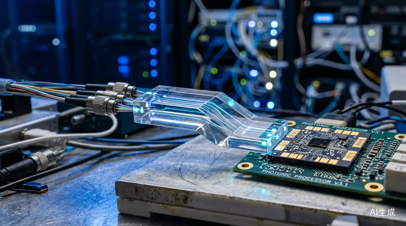
A 10,000-Word Interpretation of the "Optical Interconnect" Industry Chain: The AI Infrastructure Bottleneck Obscured by GPU Glare

marsbit05/28 11:03

τ Scaling: Huawei's New Growth Engine Designed for the Post-Moore Era

**Tau Scaling: Huawei's New Growth Engine for the Post-Moore Era** For 60 years, progress in semiconductors was driven by Moore's Law – making transistors smaller, denser, and cheaper. This path has now stalled due to plummeting returns below 7nm, astronomical lithography costs, and rising per-transistor expenses. After six years and testing 381 production chips, Huawei’s semiconductor team proposes a fundamental shift: **stop competing on size, start competing on time**. This is the core of their "τ (Tau) Scaling" theory. It treats *time* as the key optimization metric, compressing characteristic delays (τ) across all levels – from transistor switching (picoseconds) to data center tasks (seconds), spanning 12 orders of magnitude. **What is τ Scaling?** It holistically minimizes delay/time constants (τ) across four layers: transistors (switching speed), circuits (signal delay), chips (compute/memory access), and systems (end-to-end communication). The goal is to align optimization from process and circuit design to architecture and systems using this unified metric. **Mobile Application: LogicFolding** Without advancing the process node, this technique vertically stacks chips using ultra-precision hybrid bonding, distributing critical paths across layers ("stacking floors"). Results include a 55% transistor density increase, 41% better energy efficiency, over 40% higher SRAM frequency, and a roadmap targeting 4GHz by 2029. **AI Data Center Application: Full-Link Latency Compression** With 80% of AI cluster energy and 70% cost spent on data movement, the focus is slashing communication time. Key innovations include: 1. **Unified Bus:** Cuts multi-layer protocols, reducing remote access latency from microseconds to ~100 nanoseconds – 500x faster. 2. **Hi-ONE Optical Interconnect:** Replaces copper with fiber, enabling 8Tb/s per module and scaling distances from 1m to 100m for 10,000-chip clusters. 3. **3D Folding:** Solves the "interface bottleneck" of 2.5D packaging by vertically integrating memory, power, and optical I/O alongside compute, predicting over 100x integration density gain by 2035. **Re-fusion of Logic and Memory** The AI era, where data movement is more critical than computation, demands tight 3D integration of logic and memory, shifting industry influence towards memory and advanced packaging. **Remaining Challenges** include adapting EDA tools for 3D design, optimizing wafer-to-wafer process variation and vertical interconnect losses, and establishing new energy efficiency and benchmarking standards. **Conclusion:** The era of scaling physical dimensions is over. The era of scaling time has begun. By leveraging 3D stacking, system architecture, and interconnect optimization—rather than solely chasing advanced lithography—performance and efficiency can continue to advance. This is poised to be the semiconductor industry's core roadmap for the next decade.

marsbit05/25 05:35

τ Scaling: Huawei's New Growth Engine Designed for the Post-Moore Era

marsbit05/25 05:35

活动图片