EUV, which was once only affordable for TSMC, Samsung, and Intel, is now appearing on the expansion lists of Nanya Technology and Winbond Electronics. Meanwhile, a group of startups founded just two or three years ago are attempting to bypass traditional EUV lithography machines using X-rays, particle accelerators, and even helium atoms. Recently, we also reported that Elon Musk seems to be interested in putting FEL into mass production. For details, refer to the article "Musk, About to Disrupt EUV Lithography?"
It seems that almost everyone can set their sights on and utilize the EUV era overnight. Is the barrier to EUV really disappearing?
The Major Players in EUV Lithography
Currently, the players who have truly achieved large-scale mass production with EUV remain highly concentrated, with the core still being the five companies: TSMC, Samsung, Intel, SK Hynix, and Micron.
Among them, TSMC is one of the earliest and largest adopters of EUV commercialization. In 2019, TSMC formally introduced EUV in its N7+ process and achieved commercial mass production. Subsequent advanced nodes like N5 and N3 further increased the number of EUV exposure layers, and EUV gradually evolved from initial use in a few critical layers to becoming the core tool for advanced logic manufacturing.
Samsung Electronics is advancing EUV on both advanced logic and DRAM product lines. In addition to advanced process foundry services, Samsung has introduced EUV into the mass production of 14nm-class and 12nm-class DRAM, enabling EUV's gradual entry from advanced logic into memory chip manufacturing.
Intel's adoption of EUV was relatively later but is progressing rapidly. Intel 4 became its first process to adopt EUV on a large scale, with subsequent Intel 3 and 18A continuing to expand its application. Meanwhile, Intel is also one of the earliest chipmakers to receive and deploy ASML's High-NA EUV equipment, conducting early-stage technology verification for next-generation processes like 14A.
Among memory manufacturers, SK Hynix began introducing EUV into the mass production of 1a-nm-class DRAM in 2021 and has since continuously expanded its usage. In 2025, the company installed High-NA EUV equipment at its M16 wafer fab in South Korea, bringing the new generation of EUV technology into the DRAM R&D and future mass production system ahead of schedule.
Micron is the last among the three major DRAM manufacturers to formally adopt EUV. It first adopted EUV on a large scale in its 1γ (1-gamma) DRAM node and began advancing related product mass production in Taiwan, China, and Japan from 2025 onwards.
Therefore, although EUV has been developed for many years, in terms of actual high-volume manufacturing, its players are still highly concentrated in these five companies. For a considerable period in the past, whether a semiconductor manufacturer could enter this "club of five" somewhat represented whether it possessed the most advanced process manufacturing capability.
But now, this long-closed "club of five" is beginning to see new entrants.
The most typical example is Japan's Rapidus.
Established in 2022, compared to giants like TSMC, Samsung, and Intel with decades of advanced process experience, Rapidus can almost be called a "new fab." Yet, just such a company founded only a few years ago has directly stepped into the EUV era.
In December 2024, an ASML NXE:3800E EUV lithography machine arrived at Rapidus's IIM-1 wafer fab in Chitose, Hokkaido. Rapidus stated that this is Japan's first EUV exposure equipment for advanced chip mass production. Subsequently, in April 2025, the company completed its first EUV exposure and put the equipment into trial production and verification for the 2nm GAA process, aiming to achieve mass production of 2nm chips in 2027.
The uniqueness of Rapidus lies in the fact that it almost skipped the long upgrade path of traditional fabs, which gradually evolve from mature processes to advanced processes before introducing EUV. Instead, from the very beginning of its establishment, it directly built its production system around 2nm, GAA, and EUV.
This also illustrates one thing: EUV no longer belongs solely to traditional semiconductor giants with decades of advanced process accumulation. As long as there is sufficient capital, technological cooperation, and industrial support, a newly established fab can also directly acquire EUV equipment and start from the most advanced nodes.
However, Rapidus also illustrates that EUV is still far from truly becoming "democratized."
Rapidus is not an ordinary startup that independently spent hundreds of millions of dollars to purchase an EUV lithography machine. Its backing includes massive continuous financial support from the Japanese government, an industrial alliance formed by major Japanese companies such as Toyota, Sony, NTT, NEC, and SoftBank, as well as the introduction of 2nm GAA process technology through cooperation with IBM.
In other words, Rapidus's ability to directly enter the EUV era relies on a combination of national capital, industrial alliances, overseas technology transfer, and advanced equipment procurement capability to prop up a new advanced process player.
Why Are Second-Tier Fabs Also Buying EUV?
However, the current situation is that second-tier fabs are also starting to purchase EUV.
On August 5, 2026, Nanya Technology's board of directors announced that it would further increase its 2026 capital expenditure from NT$52 billion to NT$69.7 billion, a rise of over 30%. At the same time, the company approved a capital expenditure ceiling of NT$346.6 billion for the 5A new fab from 2026 to 2029, becoming one of the largest single investment plans in Nanya Technology's history. According to Nanya's currently disclosed plan, the first-phase monthly capacity target for the 5A new fab is about 35,900 wafers, and it will gradually introduce 1B, 1C, 1D, and 1E 10nm-class DRAM processes. As the process continues to shrink, EUV will become one of the key pieces of equipment in the next-generation DRAM production system.
Meanwhile, on August 6, 2026, Winbond Electronics announced the launch of the construction plan for its second 12-inch wafer fab, P2, in Kaohsiung. According to the plan, the new fab will break ground in January 2027, begin equipment installation in early 2029, and is scheduled to enter mass production in the fourth quarter of 2029. Regarding the process roadmap, Winbond has planned very clearly: the first phase will initially adopt non-EUV processes to produce 14nm-class DRAM, and the second phase will formally introduce EUV to advance towards 12nm-class DRAM.
It is worth noting that Winbond has already started planning ahead for the long lead time of EUV equipment. Management revealed that the current EUV equipment delivery cycle takes about three to three and a half years, which means that to introduce EUV around 2029, planning for equipment, facilities, and processes must start now.
Compared to Nanya Technology, Winbond's entry sends an even more noteworthy industrial signal. The reason is that Winbond has long not been a major player in the HBM or the most advanced general-purpose DRAM market. Its core business has focused more on niche DRAM, automotive memory, industrial control, and Code Storage Flash markets.
In the past, one important prerequisite for EUV to bear extremely high equipment and process costs was that it primarily served high-value chips like CPUs, GPUs, advanced SoCs, and high-end DRAM. But when a company long entrenched in niche memory also begins planning EUV for 12nm-class DRAM, it signifies that the economic boundary of EUV is changing.
1) Technical Need: EUV is spreading from logic processes to DRAM
From TSMC, Samsung, Intel to SK Hynix and Micron, EUV initially solved the problem of "how to continue making the most advanced chips." Now, with Nanya and Winbond entering the scene, EUV is gradually assuming another role—a basic production tool that must be considered for next-generation memory processes. As advanced memory processes themselves approach the economic boundary of traditional DUV multi-patterning. Continuing to rely on 193nm immersion lithography to push to smaller sizes means more exposures, more masks, more etching and deposition steps, as well as more complex overlay control and longer production cycles. When process complexity increases to a certain level, an expensive EUV machine may actually become more economical than repeatedly stacking DUV multi-patterning.
2) Business Driver: The AI boom allows second-tier memory fabs to "digest" EUV
In the past, second-tier manufacturers dared not buy EUV because prices for niche/mature DRAM were volatile and profits were meager, making it difficult to amortize the huge depreciation of a machine costing hundreds of millions of dollars. After purchasing the lithography machine, supporting infrastructure such as fab buildings, masks, photoresists, inspection, metrology, process development, and long-term maintenance are also needed. For a second-tier memory manufacturer with cyclical product prices and gross margins consistently lower than leading players, this was not an easy investment decision to make.
Especially during past memory downturns, when DRAM prices plummeted and capacity utilization dropped, manufacturers first considered cutting capital expenditures rather than purchasing the most expensive semiconductor equipment.
AI has changed this investment logic. Samsung, SK Hynix, and Micron have shifted a large amount of general-purpose DRAM capacity to produce HBM, leading to a severe supply shortage in the traditional/niche DRAM market and a sharp rise in prices. To secure long-term supply for edge AI, automotive MCU/SoC, industrial control, and AI server auxiliary memory, customers proactively signed 3~5 year long-term agreements (LTAs) with second-tier manufacturers. Higher product gross margins + long-term, predictable capacity utilization have given "second-tier/niche players" like Nanya and Winbond excellent cash flow and capital expenditure forecasting capabilities, finally enabling them to cross the "financial threshold" of EUV.
This is actually a very important change: EUV hasn't suddenly become cheaper, but memory chips have become more valuable.
In the past, a second-tier memory manufacturer might have asked: "Are we qualified to buy EUV?" Now they need to consider more: "If we don't buy EUV, can we still maintain cost competitiveness in five years?"
3) Tool Attribute Change: Low-NA EUV is becoming a relatively mature standard equipment
Another easily overlooked reason is that the EUV equipment itself has changed. The first-generation 0.33 NA EUV machines (like NXE:3400C/3600D/3800E) have undergone nearly a decade of mass production trials. Their source power, pellicle lifetime, and production line availability have already reached commercial maturity levels above 90%~95%.
This is evident from ASML's sales changes in recent years. 2019 was a key year when EUV truly entered high-volume manufacturing; ASML sold 26 EUV systems that year. Sales increased to 31 units in 2020 and further to 42 units in 2021. Recognized revenue was for 40 units in 2022 and reached 53 units in 2023. Although affected by customer capital expenditure cycles, equipment acceptance, and High-NA adoption pace, the figures for 2024 and 2025 were 44 and 48 units respectively, not a simple linear year-on-year increase. However, EUV has stably entered the stage of delivering tens of units per year.
Moreover, ASML clearly stated in 2026 that the company is pushing to achieve an output capability of at least 60 Low-NA EUV machines this year and plans to further increase it to at least 80 units in 2027. At the same time, the company continues to improve its production line move rate to meet the growing EUV demand from advanced logic and DRAM customers.
As top logic fabs (TSMC, Intel) begin moving towards 0.55 High-NA EUV, Low-NA EUV has effectively retreated to become the "second-top-tier" standard infrastructure. For DRAM manufacturers and second-tier fabs, today's Low-NA EUV is like the immersion ArFi (193nm) lithography machines of ten years ago—technical risks have been smoothed out by predecessors, and buying it means it can be directly put into production as "standard equipment."
So, technologically, DRAM increasingly needs EUV; economically, the AI boom enables more memory fabs to digest EUV; equipment-wise, Low-NA EUV has moved from verifying feasibility to expanding capacity. The combination of these three factors ultimately drives the outward expansion of the EUV customer boundary.
Challengers Reshaping EUV and Bypassing EUV
Technologies challenging ASML are rapidly increasing, such as xLight, Inversion, Substrate, Lace, Multibeam, Canon, etc. However, most only attack a weak point in the EUV system: some replace the light source, some eliminate the mask, some use X-rays, others use atomic beams.
Based on the depth of their changes to the lithography system, they can be roughly divided into four major camps.
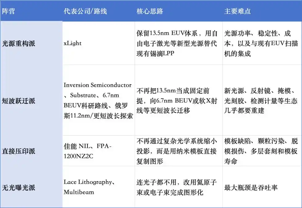
(Collated and charted by Semiconductor Industry Observation)
(I) Light Source Reconstruction Camp
This camp is trying to change the way 13.5nm EUV light is generated, aiming to solve problems like insufficient power, high energy consumption, and complex maintenance in existing laser-produced plasma sources.
The representative company is the US startup xLight. Currently, ASML's EUV systems mainly use lasers to hit tin droplets to produce plasma, which then emits 13.5nm EUV light. xLight, however, hopes to replace the current laser-produced plasma source with a Free Electron Laser (FEL), providing higher power and more stable light sources centrally for multiple EUV scanners.
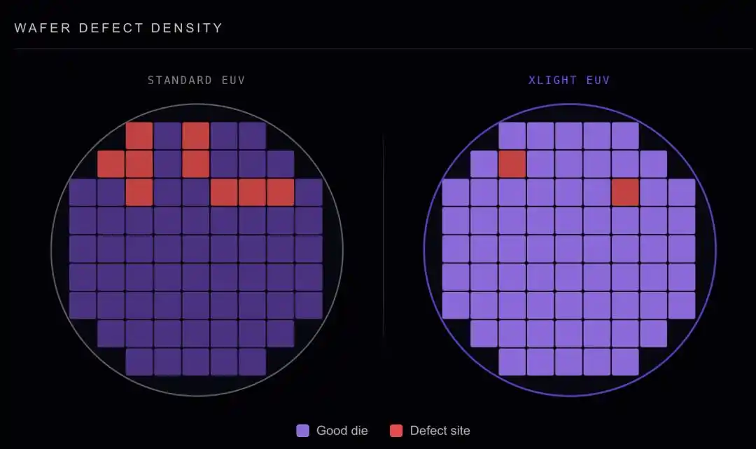
Defect distribution on the same wafer for traditional EUV vs. xLight EUV scheme (Source: xLight)
xLight mentions on its website that in a manufacturing system based on TSMC's 3nm wafer price of approximately $19,500, traditional EUV equipment costs account for 40% of the total chip manufacturing cost; whereas the FEL EUV scheme proposed by xLight can reduce EUV-related costs by 50%, lowering its share in the total cost to 20%, thereby directly reducing the total manufacturing cost of the entire wafer by 20%.
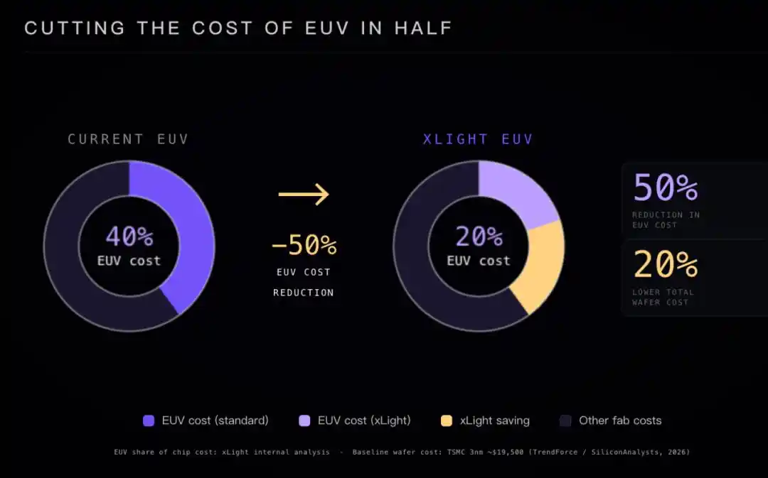
Cutting EUV costs in half (Source: xLight)
(II) Short-Wavelength Leap Camp
Today's ASML EUV lithography machines, whether the 0.33 NA NXE or the 0.55 NA High-NA EXE, still use 13.5nm EUV light. The difference is that High-NA further improves single-exposure resolution to about 8nm by increasing the numerical aperture from 0.33 to 0.55, continuing to support 2nm and subsequent logic processes.
But another group of enterprises and research institutions have begun contemplating a more radical question: even with High-NA, 13.5nm EUV will still face a series of challenges in the future regarding resolution, stochastic defects, photoresist, complex optical systems, and equipment costs. Instead of only continuously working on the numerical aperture, could we shorten the exposure wavelength further?
Thus, BEUV (Beyond EUV) and soft X-ray lithography have re-entered the field of view.
This camp includes Inversion Semiconductor, Substrate, and a series of research projects centered around 6.7nm BEUV. The technologies they adopt are not the same, but the underlying logic shares a commonality: they no longer consider 13.5nm an unchangeable constant, but attempt to migrate to shorter wavelengths, reconstructing the next-generation exposure system.
One of the most watched target wavebands is 6.5—6.7nm. From the basic relationship of lithography, exposure resolution depends on wavelength λ, numerical aperture NA, and process factor k1. Under similar other conditions, shortening the wavelength from 13.5nm to approximately 6.7nm can theoretically significantly improve resolution capability.
And 6.7nm is not a new concept that has suddenly appeared recently. As early as over a decade ago, research teams in Europe, China, Russia, and other places had already begun research on 6.7nm next-generation lithography, including plasma sources, rare-earth materials, and corresponding multilayer reflective optical systems. For example, material systems like La/B, La/B4C have long been considered important candidates for 6.7nm mirrors, with theoretical reflectivity reaching about 70%, and experimental systems have also achieved relatively high reflectivity.
Russia's exploration provides another perspective.
ASML's mainstream EUV source today uses LPP, or Laser-Produced Plasma technology: high-power CO2 lasers rapidly bombard molten tin droplets, converting them into high-temperature plasma, from which 13.5nm EUV radiation is extracted. This technology has undergone over a decade of engineering validation, but issues like tin debris, optical component contamination, energy conversion efficiency, and complex cleaning and protection systems have always been the most challenging engineering problems for EUV sources.
Therefore, some Russian research institutions have long explored gas plasma sources like xenon, hoping to bypass the tin droplet system. Unlike metallic tin, gas plasma can be exhausted through vacuum systems, theoretically reducing contamination of core optical components like collector mirrors. For more details, interested readers can click to read the previously published article "Russia Announces Breakthrough in Lithography Machines" by Semiconductor Industry Observation.
Inversion Semiconductor goes even further.
This company is developing a micro-particle accelerator based on Laser Wakefield Acceleration (LWFA), aiming to drastically shrink the originally bulky particle accelerator. Its goal is to use high-power lasers to generate extremely strong electric fields in plasma, accelerating electrons to high-energy states over very short distances, thereby producing high-power, tunable short-wavelength radiation.
Inversion's currently proposed STARLIGHT source aims to cover the band from about 20nm to 6nm. Therefore, it can generate the 13.5nm light needed for today's EUV lithography and also move further into the soft X-ray range. The ultimate goal is not just to replace ASML's tin droplet source but to build a complete next-generation lithography platform around this small particle accelerator.
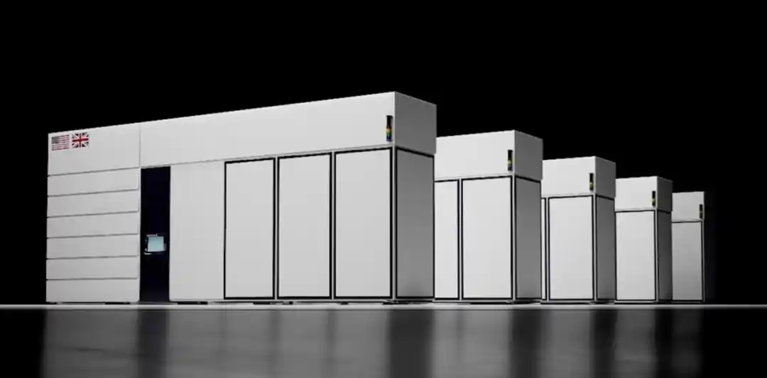
(Source: Inversion Semiconductor)
Substrate has chosen another accelerator route. It also uses high-energy electrons to generate X-rays, but the specific architecture differs from Inversion's Laser Wakefield Acceleration. Substrate accelerates electrons to near-light speed via RF cavities, then passes the electrons through alternating magnetic fields to produce extremely high-brightness X-rays, finally completing wafer exposure through new optics and high-speed mechanical systems.
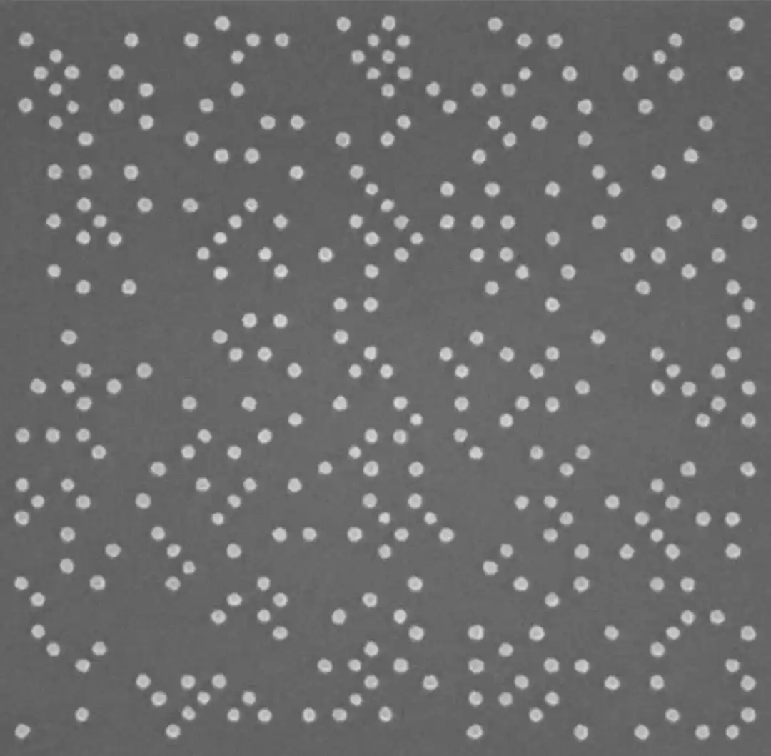
Substrate states that random via holes with a center-to-center pitch of 30nm exhibit excellent pattern quality and critical dimension uniformity (Source: Substrate)
But Substrate's ambition is not just to build a new lithography machine. It hopes to establish a more vertically integrated foundry model around this X-ray lithography technology, integrating the particle accelerator, light source, exposure equipment, and advanced wafer manufacturing within the same system.
Inversion is more like building a next-generation light source/lithography platform, while Substrate wants to use new lithography technology to reconstruct the entire foundry model.
From this perspective, ASML's current choice is "maintain 13.5nm, continue improving resolution through larger NA"; whereas Inversion, Substrate, and BEUV researchers are opening another technological variable—since NA can be changed, why can't the wavelength λ itself be changed?
However, shortening the wavelength does not mean lithography suddenly becomes simple. Once moving from 13.5nm into the 11nm, 6.7nm, or even shorter soft X-ray regions, almost the entire system of light source, mirrors, masks, photoresist, metrology, inspection, and contamination control built up for EUV today needs to be redesigned.
(III) Nanoimprint Lithography (NIL) Camp
Canon's Nanoimprint Lithography (NIL) is currently one of the non-traditional lithography routes closest to industrialization.
Traditional EUV requires generating a high-power light source first, then projecting the mask pattern onto the wafer through multiple sets of high-precision mirrors with reduction. NIL directly presses a template with nano-scale patterns onto the wafer's photoresist, similar to stamping circuit patterns. This method eliminates complex projection lenses and does not require high-power EUV sources, theoretically significantly reducing equipment cost, energy consumption, and process steps.
Canon has already launched the commercial FPA-1200NZ2C equipment, targeting 3D NAND as the first mass production application, then expanding to DRAM and logic chips.
However, NIL's difficulties are equally prominent. Because the template needs to approach or even contact the wafer, particle contamination, template defects, demolding damage, and multi-layer overlay can directly affect yield. Therefore, Canon bypasses the most critical high-power source and projection optical system of ASML but does not bypass lithography challenges like mask manufacturing, defect control, and nanometer-level overlay.
(IV) Non-Photon Exposure Camp
This camp goes even further: not only eliminating the EUV source and mirrors but also no longer using photons to complete exposure, instead using atoms or electrons to form patterns directly on the wafer.
In this regard, Lace Lithography and Multibeam are attempting to use particles like atoms or electrons directly to complete nanoscale patterning.
Among them, Lace Lithography, a startup founded in 2023, uses metastable helium atomic beam lithography. The matter-wave wavelength of helium atoms is far shorter than 13.5nm EUV light, theoretically not subject to the same diffraction limits as traditional optics. Compared to charged ions, neutral helium atoms can also reduce charging effects on the wafer surface. The essence of Lace has shifted from "photon lithography" to "matter-wave lithography." It attempts to change not just the light source but the exposure medium itself.
Multibeam takes a completely different particle route—multi-column electron beam direct write. Electron beam lithography is not a new technology. In fact, it has long been one of the highest-resolution patterning tools in the semiconductor industry and an important means for advanced photomask manufacturing, R&D, and small-batch chip production.
It has only one biggest problem, but also the most fatal one: too slow. Multibeam aims to change this bottleneck. Its idea is not to make a single electron beam write faster but to simultaneously increase the number of writing channels. By deploying multiple independent electron beam columns, multiple areas are exposed concurrently, turning the previous "single-pen drawing" into "multi-pen parallel." More importantly, electron beams can write directly based on digital layouts, unlike traditional EUV which requires making a complete set of photomasks in advance. This brings another advantage: maskless manufacturing.
Multibeam has already launched its second-generation MBX-300 multi-column electron beam lithography platform, targeting 300mm wafers and applications such as advanced packaging, silicon photonics, quantum devices, and compound semiconductors. The equipment can directly read chip layout data for writing, eliminating the need for traditional photomasks, and supports extending from prototype development to production. Its officially announced typical throughput is about 1—2 wafers per hour per writing chamber, reaching up to 25 wafers per hour in specific applications like Secure Chip ID. In 2026, Taiwan's National Tsing Hua University also ordered a new-generation MBX system for semiconductor research and joint development with chip companies.
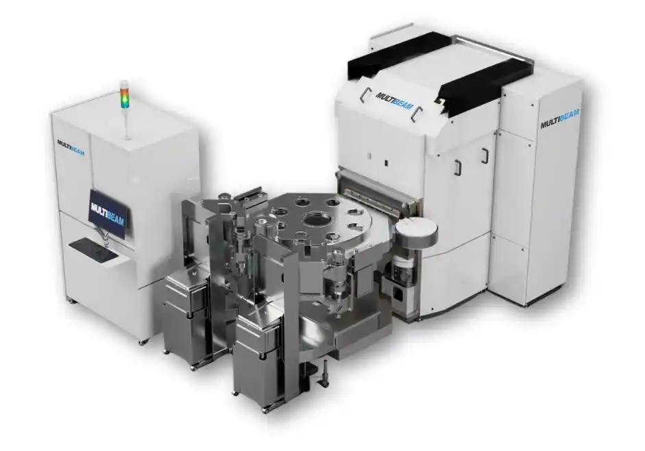
MBX Platform (Source: Multibeam)
Although both Lace and Multibeam use particles for patterning, the two routes actually address completely different problems: Lace wants to break the resolution limit: pushing pattern dimensions further down through the extremely short matter-wave wavelength of neutral helium atoms; Multibeam wants to break the efficiency limit of electron beams: pushing the originally R&D and small-batch suitable electron beam technology towards larger manufacturing scales through multi-beam parallelism, digital direct write, and maskless manufacturing.
The biggest challenge they face together is how to increase throughput to a level acceptable for advanced wafer fabs while maintaining nanoscale resolution. This also reveals the ultimate challenge faced by all EUV challengers: the real threshold of lithography has never been just resolution, but simultaneously achieving "writing finely, writing accurately, writing fast, and writing stably 24/7."
Looking overall, players challenging ASML's EUV, or more accurately, deconstructing EUV, follow this progression of four types of approaches: Change the light source → Change the wavelength → Eliminate projection → Eliminate photons.
Conclusion
Returning to the opening question: Is there really no barrier to EUV lithography machines?
The answer is clearly no.
A single EUV lithography machine still costs hundreds of millions of dollars, requiring advanced fab buildings, masks, photoresists, inspection, metrology, and long-term process accumulation and yield ramping. Neither the financial barrier nor the engineering barrier of truly turning the equipment into mass production capability has disappeared.
But another change is equally impossible to ignore: the "customer entry barrier" for EUV is indeed declining. From a top-tier luxury item for a few giants to a production necessity for niche players, the descent of EUV lithography machines reveals the new game rules as Moore's Law enters its second half. The "demystification" of EUV is accelerating.
But perhaps the bigger change is happening outside the EUV system. A technological encirclement of the "post-EUV era" is taking shape. Innovative routes challenging ASML are emerging one after another. Although the vast majority of emerging solutions are still confined to the laboratory and pilot production stages, yet to cross the chasm of extremely high yield, stable uptime, and vast ecosystem required by "High Volume Manufacturing (HVM)," their very existence has already torn open a small crack for the expensive traditional lithography technology.
Departing from absolute monopoly does not mean individual breakthroughs are easily attainable. It is foreseeable that the future lithography market may no longer be dominated solely by ASML. A new ecosystem of diversified competition, where standard Low-NA EUV fills the mid-range, cutting-edge High-NA EUV builds the top, and emerging routes break through in niche segments, is on the horizon.
This article is from the WeChat public account "Semiconductor Industry Observation" (ID: icbank), author: Du Qin DQ.