SemiAnalysis Dissects Huawei's Kirin 9030: Process Technology Halted, So They Folded the Chip

marsbitОпубліковано о 2026-06-15Востаннє оновлено о 2026-06-15

Анотація

SemiAnalysis has published a detailed teardown report on the HiSilicon Kirin 9030 Pro chipset found in Huawei's Mate 80 Pro. Fabricated using SMIC's most advanced N+3 node without EUV lithography, the analysis reveals significant technical achievements and strategic shifts. The report indicates SMIC's N+3 has achieved transistor density comparable to TSMC's N6 (113.4 vs 107.7 MTr/mm²), primarily through aggressive use of Self-Aligned Quadruple Patterning (SAQP) for its metal layers. This results in a notably small 32.5nm M0 metal pitch. However, SemiAnalysis notes this achievement comes with significantly higher process complexity, cost, and potential yield challenges compared to competitors using more advanced tools. The Kirin 9030 design maximizes this constrained density. While its GPU performance has improved ~70% and matches Qualcomm's 2022 flagship level, the CPU core's IPC lags behind current top-tier designs from Apple and Qualcomm, a gap attributed to the underlying manufacturing technology rather than design capability. Facing long-term restrictions on advanced tools, Huawei is charting a new path. The report highlights the company's "LogicFolding" roadmap, a 3D stacking technique aimed at shortening signal paths to boost performance and efficiency. The goal is to reach 5GHz frequency and a projected density of 295 MTr/mm² by 2031. SemiAnalysis concludes that export controls have not halted China's chip progress but have fundamentally altered its trajectory, mak...

Author: Tide Research

In the field of semiconductor reverse engineering, TechInsights had dominated for decades. Last weekend, Dylan Patel's SemiAnalysis officially released the first public teardown report from its STEEL lab (Teardown Engineering & Evaluation Lab), targeting one of the world's most-watched chips: the Kirin 9030 Pro, manufactured on SMIC's most advanced N+3 process, which powers the Huawei Mate 80 Pro.

The timing is intriguing. While TechInsights is being sold by private equity, SemiAnalysis' revenue has already surpassed that of this established giant. Dylan chose this moment to demonstrate its capabilities with a technically dense teardown report, complemented by real chip photos from its Oregon lab.

The report's headline is a bombshell: SMIC's N+3 process features a minimum metal pitch (M0 pitch) of only 32.5nm, smaller than the 36nm pitch of Intel's latest Panther Lake processors using the 18A process.

SMIC, without EUV lithography machines, achieved a finer metal pitch than Intel?

On its own, this headline could send shockwaves through the semiconductor industry. However, SemiAnalysis itself pours cold water on it in the report's second paragraph, calling it a "cherry picked metric."

This article will interpret this teardown report for you.

Catching Up in Density, at a High Cost

SMIC's N+3 process has indeed caught up with TSMC's N6 in terms of transistor density.

Through TEM (Transmission Electron Microscopy) cross-sectional analysis, STEEL Lab measured the Bohr density of N+3 at 113.4 MTr/mm², slightly higher than TSMC N6's 107.7 MTr/mm². The cell height shrank from 252nm in N+2 to 228nm, and the contacted gate pitch (CGP) reduced from 63nm to 57nm. Taken together, these numbers mean that SMIC, using pure DUV lithography without EUV, has achieved logic density comparable to TSMC's mature 7nm-class processes.

At what cost?

SMIC's M0 layer uses Self-Aligned Quadruple Patterning (SAQP), where a single photomask pattern undergoes four processing steps to achieve finer lines. TSMC's N6 requires only Double Patterning (SADP) for the same layer. Quadruple patterning means more mask counts, stricter overlay accuracy requirements, more complex process flows, and higher costs.

SemiAnalysis directly observed the consequence of SAQP in the cross-sectional images: the M0 trenches of N+3 show a pronounced inverted trapezoid profile (narrower at the bottom than the top), with a clear barrier layer enrichment zone at the trench bottom. While this morphology aids copper filling, the difficulty of process control skyrockets at this 32.5nm pitch.

To use a trader-friendly analogy: SMIC is printing banknotes of the same denomination, but each note costs multiples more to print than TSMC's, with greater yield risk. The density is the same, but the economics are entirely different.

Kirin 9030: Squeezing Every Square Millimeter of Silicon Under Constraints

HiSilicon's chip design prowess is another story.

Looking at die area, the Kirin 9030 is almost the same size as its predecessor, the 9020 (around 140mm²), but packs in more: the CPU upgraded from 1 big core + 3 medium cores to 1 big + 4 medium, GPU compute units increased from 4 to 6, an extra Tiny core was added to the NPU, and caches were expanded across the board. The density improvement from N+3 allowed Huawei to cram more logic into the same die size.

On performance, STEEL Lab referenced public benchmark data, offering a clear positioning: the Kirin 9030's GPU performance (Mali-G935) roughly matches flagship levels from 2022. Its 3DMark WLE score improved 70% over the previous generation, slightly surpassing the Snapdragon 8+ Gen 1, but compared to the current flagship Snapdragon 8 Elite Gen 5, the gap is 2.4x to 2.6x.

The CPU situation is more telling. The IPC of the big core, TaiShan Prime, is roughly at the level of Arm's Cortex-X2, a 2021 design. The IPC of Apple's M1 Firestorm core, released in 2020, remains 35% higher. The latest Apple M5 P-core's IPC is 60% higher, with absolute performance being 2.7x that of the Kirin core.

The root of the gap lies not in design, but in process technology. Apple and Qualcomm use TSMC's N4, N3P, processes that have fundamental advantages in the voltage-frequency curve: more transistors can be packed into the same area, higher frequencies can be achieved at the same power. Huawei's core designs are on par with the industry's previous generation leaders, but are trapped in manufacturing processes two generations behind.

When Process Scaling Stalled, Huawei Prepares to "Fold"

The most forward-looking part of the report is Huawei's τ scaling law and LogicFolding roadmap, presented at the 2026 ISCAS conference.

Traditional semiconductor scaling advances on a two-dimensional plane: shrinking transistors and narrowing metal lines. Moore's Law has progressed for decades, essentially doing just that. The τ scaling Huawei proposes shifts the optimization target from the spatial domain to the temporal domain, focusing on reducing time costs for data movement and processing, including transistor switching delay, signal propagation delay, and compute/memory access latency.

LogicFolding is the engineering implementation of this theory. Simply put, it splits the same logic block into top and bottom layers, stacking them face-to-face and connecting them via ultra-fine-pitch hybrid bonding. The direct benefit is shortening the longest signal paths. In modern chips, a significant portion of power and delay is spent driving long interconnects and repeater buffers. By folding logic vertically, critical paths become shorter, enabling higher frequencies and lower power consumption.

Huawei outlined an aggressive roadmap: While the Kirin 9030's big core runs at 2.75GHz, lab samples have achieved 3.39GHz, with a target of reaching 5GHz by 2031. Concurrently, through 3D stacking, the equivalent density aims to reach 295 MTr/mm², comparable to TSMC's 14A level.

SemiAnalysis remains skeptical. They point out that Huawei's density calculation method differs from traditional foundries: the density for 3D stacking is calculated based on package footprint, naturally yielding higher numbers when stacking multiple active logic layers. Using the same method to calculate AMD's MI450X (N2 top die + N3P base die) would yield a theoretical density of 460.2 MTr/mm², far exceeding Huawei's 2031 target.

However, the direction itself warrants attention. For Huawei, this path essentially involves a systems design company taking on tasks traditionally handled by foundries. AMD's V-Cache implements 3D stacking for cache, and AMD MI350X moves I/O and interconnects to the base die. What Huawei aims to do is more radical—directly splitting a single logic block and distributing it vertically. This represents a challenge of another magnitude in engineering difficulty.

Export Controls Reshape the Dimensions of the Race

SemiAnalysis' concluding point is blunt: Export controls have not stopped China's chip progress, but they have altered the path and the cost of that progress.

SMIC's N+3 proves that N6-level logic density can be achieved without EUV. But this path is more expensive, more complex, and has greater yield challenges. Every step forward increases the marginal difficulty: more masks, stricter overlay control, more costly multiple patterning. Theoretically, N+4 could reach 137.8 MTr/mm² (comparable to TSMC N5), and N+5, with the introduction of backside power delivery, could even approach Intel 18A's HP library density. But each step is harder, more expensive, and has less margin for error than the last.

Meanwhile, SMIC's N+2 and N+3 processes are being transferred to Huahong, potentially benefiting design houses like Alibaba's T-Head and Cambricon. Chip manufacturing knowledge is diffusing from a single foundry to an ecosystem, further diluting the effectiveness of sanctions against individual companies.

On the design side, Huawei and Peking University are already developing domestic EDA tool prototypes for LogicFolding. This doesn't equate to replacing the complete toolchains of Synopsys and Cadence, but domestic EDA is evolving towards "architecture-process-packaging co-optimization."

An interesting detail: STEEL found in its teardown that the DRAM in the Kirin 9030 Pro comes from Samsung (K4L2E165YD, LPDDR5X-9600, 1a node), while the 16GB Pro Max version shows packages from both Samsung and ChangXin Memory (CXMT). The CXMT chip packaging date is marked as week 45 of 2025, with process density equivalent to the industry's 1z level. This indicates that Chinese memory chips have begun entering Huawei's flagship supply chain, albeit still one to two generations behind Samsung and SK Hynix in process technology.

For investors, the signal truly worth tracking is whether Huawei's 3D stacking roadmap can, at a controllable cost, bring Chinese-produced chips to a "good enough" threshold for scenarios like smartphones, AI inference, and networking equipment.

Once "good enough" is established, the strategic value of this supply chain will be repriced.

Трендові криптовалюти

Пов'язані питання

QAccording to the article, what is the key manufacturing cost disadvantage for SMIC's N+3 process compared to TSMC's N6, despite achieving similar transistor density?

AThe key disadvantage is that SMIC's N+3 process uses Self-Aligned Quadruple Patterning (SAQP) for its M0 layer, while TSMC's N6 uses Self-Aligned Double Patterning (SADP). This means more mask layers, stricter overlay accuracy requirements, a more complex process flow, and significantly higher manufacturing costs for SMIC to achieve a similar density.

QWhat is the primary architectural innovation that Huawei is proposing for its future chip roadmap to overcome limitations in 2D process scaling?

AHuawei is proposing LogicFolding, a form of 3D stacking where a single logical block is split and distributed across two layers, connected by ultra-fine pitch hybrid bonding. This aims to shorten critical signal paths, reduce power consumption, and enable higher frequencies.

QWhat metric did SemiAnalysis use to measure transistor density for SMIC's N+3 process, and how did it compare to TSMC's N6 process?

ASemiAnalysis's STEEL Lab measured SMIC's N+3 process using the Bohr density metric, finding it to be 113.4 MTr/mm², which is slightly higher than TSMC's N6 process density of 107.7 MTr/mm².

QWhat is the main conclusion of the article regarding the effect of export controls on China's semiconductor advancement?

AThe main conclusion is that export controls have not stopped China's chip progress, but they have fundamentally changed its path and increased its cost. China is advancing by using more complex and expensive multi-patterning techniques without EUV and by exploring architectural innovations like 3D stacking to compensate for process limitations.

QWhat evidence from the chip teardown suggests China's domestic memory chip production is entering the flagship supply chain, and what is its relative maturity level?

AThe teardown of the 16GB Pro Max version of the Mate 80 Pro found DRAM chips from both Samsung and China's ChangXin Memory (CXMT). CXMT's chip package was dated the 45th week of 2025, and its process density was equivalent to the industry's 1z generation. This indicates it has entered Huawei's flagship supply chain but remains one to two generations behind Samsung and SK Hynix.

Пов'язані матеріали

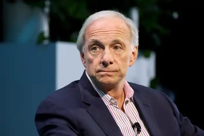
In Conversation with Ray Dalio: We Are Currently in an AI Bubble, with 1% of My Portfolio in Bitcoin

Ray Dalio, founder of Bridgewater Associates, warns in an interview that the current AI boom shows classic bubble characteristics, which could lead to significant economic downturns as seen in past cycles like 1929 or 2000. He explains that speculative enthusiasm, fueled by debt and overvaluation, often precedes a crash when rising rates or taxation force asset sales, causing widespread losses and recession. Dalio also outlines his "Big Cycle" theory, describing an approximate 80-year pattern where widening wealth gaps, massive government deficits, and shifting geopolitical power (like China's rise) create internal conflict and global instability. He emphasizes that we are in a late-cycle, transitional phase where traditional powers like the US and UK face decline. For personal wealth protection, Dalio advises diversification beyond cash into assets like stocks, bonds, real estate, and particularly gold, which he prefers over Bitcoin. While he holds about 1% of his portfolio in Bitcoin as a non-printable hard asset, he views gold as more secure from technological or governmental threats. Regarding AI's impact, Dalio believes it will disproportionately benefit capital owners, worsening inequality by replacing both physical and cognitive labor. He suggests that human intuition and emotional intelligence, combined with AI, will be key for future workers. On taxation, Dalio argues that wealth taxes are impractical and risk triggering asset sell-offs, reducing productive investment. He points to the UK as a cautionary example of debt, low productivity, and political strife. Geopolitically, Dalio foresees a more regionalized world, with the US showing weakness in prolonged conflicts like with Iran, akin to past imperial declines. The ideal outcome, he suggests, is coexisting powerful blocs (e.g., Americas, China-Asia Pacific) without major war.

marsbit39 хв тому

In Conversation with Ray Dalio: We Are Currently in an AI Bubble, with 1% of My Portfolio in Bitcoin

marsbit39 хв тому

Daily 7.2 Trillion KRW: Foreign Capital's Record Net Buying on Friday! Wall Street Says Headwinds for Korean Stock Fund Flows Have Subsided

South Korean stock market sees a dramatic shift in fund flows. On July 31, foreign investors made a record net purchase of approximately KRW 7.2 trillion in KOSPI stocks, marking a fundamental reversal from the persistent large-scale net outflows seen in previous months. This contributed to a significant narrowing of foreign net selling in July to KRW 9.8 trillion, down sharply from KRW 48.4 trillion in June and KRW 44.5 trillion in May. Simultaneously, domestic institutional pressure eased. South Korean pension funds and asset managers turned to a net buying position in July, purchasing KRW 1.0 trillion worth of KOSPI shares, contrasting with net sales in May and June. Market volatility is expected to be dampened by new financial regulations. Effective July 31, the Financial Services Commission tightened access for retail investors to single-stock leveraged ETFs by raising the minimum cash deposit requirement. Trading volumes for these products subsequently dropped to about 50% of their monthly average. Citigroup Research maintains its year-end KOSPI target of 10,000 points. The firm cites several supportive factors: the substantial easing of headwinds from capital outflows, a robust fundamental outlook for the semiconductor sector, historically low market valuations, strong economic fundamentals, and the potential for policy support from financial authorities if needed.

marsbit39 хв тому

Daily 7.2 Trillion KRW: Foreign Capital's Record Net Buying on Friday! Wall Street Says Headwinds for Korean Stock Fund Flows Have Subsided

marsbit39 хв тому

Thanks to Dice Rolls, Bitcoin Keys Are Stored Offline, But Not Everyone Will Do It

The article discusses using dice rolls to generate secure Bitcoin wallet seeds, providing entropy independent of potentially flawed hardware random number generators. It explains that each fair dice roll offers about 2.585 bits of entropy, with around 50 rolls needed for a standard 12-word seed phrase and 99+ recommended for higher security. This method gained attention after a vulnerability was revealed in some Coldcard hardware wallets, where a faulty firmware RNG (dating back to 2021) compromised generated keys. The analysis notes that while a dice-generated main seed was safe from this specific flaw, other Coldcard functions (like creating paper wallets, backup keys, or passwords) could still be vulnerable if they used the defective RNG. The piece argues that while dice-based entropy is technically robust, the manual process is error-prone, tedious, and unrealistic for most new users, who might make mistakes in recording or inputting rolls. It concludes that while manual entropy generation should remain an option for advanced users, the long-term goal is to develop reliable, user-friendly hardware and software that securely generates randomness without requiring specialized knowledge. Coldcard users are advised to check their firmware version and replace any secondary secrets (like paper wallet keys) created with vulnerable devices, while also considering multi-signature setups with devices from different manufacturers for added security.

cryptonews.ru5 год тому

Thanks to Dice Rolls, Bitcoin Keys Are Stored Offline, But Not Everyone Will Do It

cryptonews.ru5 год тому

Торгівля

Спот

Популярні статті

Як купити CHIP

Ласкаво просимо до HTX.com! Ми зробили покупку USD.AI (CHIP) простою та зручною. Дотримуйтесь нашої покрокової інструкції, щоб розпочати свою криптовалютну подорож.Крок 1: Створіть обліковий запис на HTXВикористовуйте свою електронну пошту або номер телефону, щоб зареєструвати обліковий запис на HTX безплатно. Пройдіть безпроблемну реєстрацію й отримайте доступ до всіх функцій.ЗареєструватисьКрок 2: Перейдіть до розділу Купити крипту і виберіть спосіб оплатиКредитна/дебетова картка: використовуйте вашу картку Visa або Mastercard, щоб миттєво купити USD.AI (CHIP).Баланс: використовуйте кошти з балансу вашого рахунку HTX для безперешкодної торгівлі.Треті особи: ми додали популярні способи оплати, такі як Google Pay та Apple Pay, щоб підвищити зручність.P2P: Торгуйте безпосередньо з іншими користувачами на HTX.Позабіржова торгівля (OTC): ми пропонуємо індивідуальні послуги та конкурентні обмінні курси для трейдерів.Крок 3: Зберігайте свої USD.AI (CHIP)Після придбання USD.AI (CHIP) збережіть його у своєму обліковому записі на HTX. Крім того, ви можете відправити його в інше місце за допомогою блокчейн-переказу або використовувати його для торгівлі іншими криптовалютами.Крок 4: Торгівля USD.AI (CHIP)Легко торгуйте USD.AI (CHIP) на спотовому ринку HTX. Просто увійдіть до свого облікового запису, виберіть торгову пару, укладайте угоди та спостерігайте за ними в режимі реального часу. Ми пропонуємо зручний досвід як для початківців, так і для досвідчених трейдерів.

650 переглядів усьогоОпубліковано 2026.04.21Оновлено 2026.06.02

Як купити CHIP

Обговорення

Ласкаво просимо до спільноти HTX. Тут ви можете бути в курсі останніх подій розвитку платформи та отримати доступ до професійної ринкової інформації. Нижче представлені думки користувачів щодо ціни CHIP (CHIP).

活动图片