ChipNews August 19 report - On August 5, Japanese household and personal care giant Kao Corporation released its interim report for the fiscal year 2026. Within the financial report of this company famous for laundry detergent and facial cleanser, a business line less known to the general public became the core growth driver—semiconductor precision cleaning agents.
The financial report shows that in the semiconductor back-end process, Kao holds an approximate 60% market share in precision cleaning agents for package substrates; in the front-end process, Kao holds the top share in chemicals used for specific NAND manufacturing processes.
During the same period, Kao's chemical business, which includes semiconductor precision cleaning agents, achieved net sales of 247.2 billion yen (approximately 10.44 billion RMB), a year-on-year increase of 9.4%. This growth rate is more than double that of Kao's consumer goods business, making it the fastest-growing segment for the period. Currently, Kao's cleaning agents have entered the supply chains of leading semiconductor companies such as TSMC, Samsung, and Kioxia.
In the earnings conference call on August 5, Kao executives stated that the company is shifting its focus toward high-value-added businesses like electronic materials and semiconductor-related products. Its front-end chemicals business is expanding from NAND to the currently hotter areas of DRAM and logic semiconductors.
How did a company famous for cleaning agents and personal care products manage to secure a leading position in the high-barrier semiconductor materials segment?
01. Starting from a bar of soap, entering the precision cleaning market in the 1990s
In 1887, Kao's founder, Tomiro Nagase, opened a general store named "Nagase Store" in Tokyo, primarily selling various Western sundries, with soap being a major category.
At that time, soap in Japan mainly relied on imports and was expensive, while domestically produced soap was of poor quality. Tomiro Nagase saw the opportunity and, three years later, developed a reasonably priced, high-quality facial soap. This soap was later named "Kao," from which the company derived its name.

Kao's founder, Tomiro Nagase, and Kao's soap products
The soap business soon hit a ceiling: raw materials. The core of soap is fat, and deep processing technology for fats was held by European and American manufacturers. To avoid being constrained by raw materials, in 1925, Kao's Tokyo factory began production, achieving large-scale glycerol production; in 1928, Kao created Japan's first food industrial shortening, expanding the application of fats from soap to food. The fat chemistry business, originally derived from soap making, gradually grew into an independent venture.
In 1951, Kao began selling surfactants, the core component of synthetic detergents, which also became the origin of the later "Kao Chemicals" business. Surfactants can manipulate everything that happens when a liquid contacts a solid: wetting, penetration, dispersion, and stripping. Mastering this skill gave Kao a ticket to almost all "interface problems."
In the following decades, Kao's chemical business expanded along this line: in the 1960s, its developed polyurethane catalysts and concrete admixtures were applied in highway and high-rise building construction; the wastepaper deinking agent launched in the 1970s caught the wave of recycled paper; and the photocopier toner binder from the 1980s rode the wave of office automation. The industries these products belonged to seemed unrelated, but the core was always interface control.
Kao's intersection with semiconductors began with an industry reshuffle triggered by environmental regulations. Freon was the mainstream solvent for circuit board and precision component cleaning at the time. It performed well, was volatile, and non-flammable, and the entire industry was deeply reliant on it. However, with the signing of the Montreal Protocol in 1987, ozone-depleting chlorofluorocarbons (represented by Freon, etc.) entered a phase-out countdown.
Under the ban, alternatives had to simultaneously meet several nearly contradictory conditions: capable of removing grease and flux residue, non-corrosive to metals and resins, easy to rinse off, and waste liquid must be treatable. Various alternative solvents that emerged subsequently each had significant shortcomings, plunging the industry into a dilemma of "compliant ones don't work well, effective ones aren't compliant."
This was precisely Kao's strength. One of the core contradictions in household and personal care product development is balancing cleaning power with mildness. Kao's accumulation in raw material purification and low-residue formulations also aligned with the purity requirements of electronic cleaning.
In 1991, Kao launched the CLEANTHROUGH water-based cleaning agent, replacing Freon with a surfactant compound system, entering the precision cleaning market, and accumulating process data and customer relationships for future entry into semiconductor cleaning.
02. Products cover front and back-end semiconductor processes and extend to adjacent steps
Over the next thirty-plus years, Kao's CLEANTHROUGH product line continuously expanded along the path of electronics manufacturing advancement. In 2001, Kao began production of polishing agents for Hard Disk Drive (HDD) platter manufacturing, extending products from cleaning to the polishing process. Subsequently, as chip processes continued to shrink, its cleaning targets upgraded from circuit boards to wafers, gradually establishing a product system covering silicon wafer rinsing, particle removal, wettability improvement, and photoresist stripping, with corresponding products for almost every cleaning step.
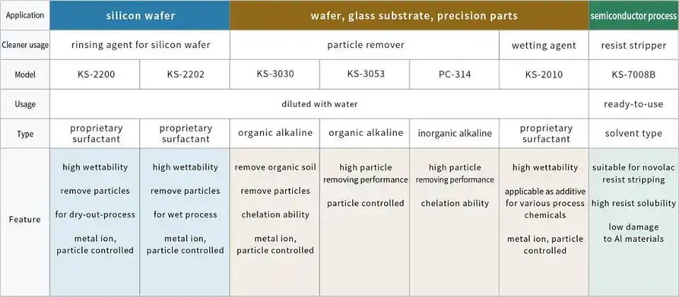
Supporting these products is what Kao calls its "Precision Interface Control Technology." In principle, its core is achieving uniformity of the cleaning action on complex nanostructures while maintaining selectivity towards various materials, and meeting the semiconductor industry's specifications for purity, particle control, and metal impurity management.
Specifically, in the front-end wafer manufacturing process, cleaning accounts for about 30% of the total steps. Advanced processes have low tolerance for particles, metal ions, and organic residues, where excess residue can significantly impact product yield. Traditional RCA cleaning relies on multiple cycles of strong chemicals like hydrogen peroxide, sulfuric acid, ammonia, and hydrofluoric acid, facing issues such as wafer surface damage, high water and electricity consumption, and heavy waste liquid processing burdens.
Kao's entry point was the pre-cleaning and rinsing chemical series KS-2200 for silicon wafers: after a 300mm wafer is polished with silicon dioxide abrasive, the number of particles adhering to the surface, according to Kao's estimates, reaches about 7 trillion. Moreover, the silicon surface is naturally hydrophobic, making it difficult for chemicals to wet uniformly. The KS-2200 series modifies the surface to be super-hydrophilic, improving wettability so that a water film spreads evenly, mechanically suppressing particle adhesion and thus reducing the number of cleaning cycles.
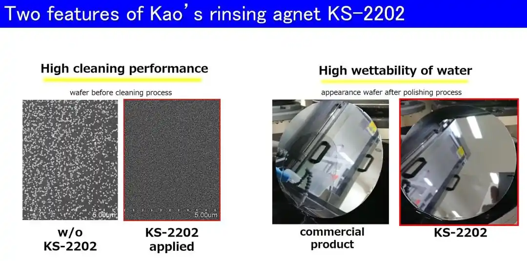
Another key indicator for particle removal is preventing recontamination. Kao's KS-3000 series targets scenarios like post-CMP cleaning, photomasks, and quartz fixtures. It enhances the dispersion stability of particles through surfactants and adjusts the particle surface Zeta potential to create electrostatic repulsion, inhibiting redeposition of already removed particles like silicon dioxide and cerium dioxide during the rinsing process.
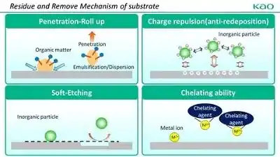
In photoresist removal, Kao's KS-7000 series uses a swelling and stripping mechanism rather than chemical dissolution, reducing the risk of damage to underlying metal lines; semi-aqueous wetting agents like KS-2010 are used to improve chemical infiltration in narrow-gap structures.
The packaging segment is where Kao holds its highest market share. High-end ABF substrate line width/spacing has entered below 10 micrometers, with micro-via structures being deep and narrow. Drilling residue, plating residue, and flux, if not thoroughly removed, can cause short circuits or reliability failures due to ion migration.
The difficulty in this segment lies in selectivity: a single substrate contains multiple materials like copper, resin, nickel, and gold. The cleaning agent must penetrate microstructures to remove contaminants without corroding any substrate material, and must itself be easy to rinse off with extremely low ionic residue.
Kao has highly segmented this area, with each product addressing a specific process pain point. Rosin-based solder paste and flux residue are the most common contaminants in packaging cleaning. Kao's solution is CLEANTHROUGH 750H, a cleaning agent for high-density packaging components with OSP (Organic Solderability Preservative) coating, covering mainstream packaging forms like BGA, CSP, WLCSP, PiP, PoP. It dissolves residue without damaging the OSP film itself.
Another pain point occurs after cleaning: copper OSP pads are prone to discoloration during cleaning, affecting subsequent soldering reliability. The 770A was developed specifically for this issue. With the expansion of power semiconductors, cleaning targets have further extended to sintered materials and high-melting-point solder in power modules, for which Kao has also configured dedicated product lines.
Beyond cleaning, Kao's product portfolio extends to adjacent process steps. The substrate circuit patterning and solder bump processes require stripping of dry film photoresist. Kao provides strippers, including amine-free formulations, the latter giving customers leeway for wastewater treatment. In 2.5D/3D packaging, stubborn residue left by temporary bonding materials after high-temperature or laser treatment was once a bottleneck for mass production. Matching cleaning agents are also on Kao's product list.
03. Directly participating in customer process development, positioning for AI-driven capacity expansion wave
Kao's foothold in the semiconductor industry relies not only on products but also on a commercial system built around customer production lines.
The semiconductor materials business model has a characteristic: once a product passes customer verification and enters mass production, the cost of switching suppliers is extremely high. Changing cleaning chemicals means redoing a full set of reliability verifications, which is time-consuming and carries yield risks. Therefore, leading suppliers' shares typically have strong stickiness.
To leverage this industry characteristic, Kao has established Fine Cleaning Centers in Wakayama, Japan, and Hsinchu, Taiwan, China, opening up actual cleaning and stripping process testing and analysis to customers, participating in their process development rather than just selling chemicals.
The Hsinchu Center in Taiwan, China, launched in December 2025, is Kao's first overseas cleaning center. Officially disclosed service targets include PCB, IC substrate, automotive and communication substrate manufacturers, as well as advanced packaging lines like CoWoS, CoWoP, and FOPLP.
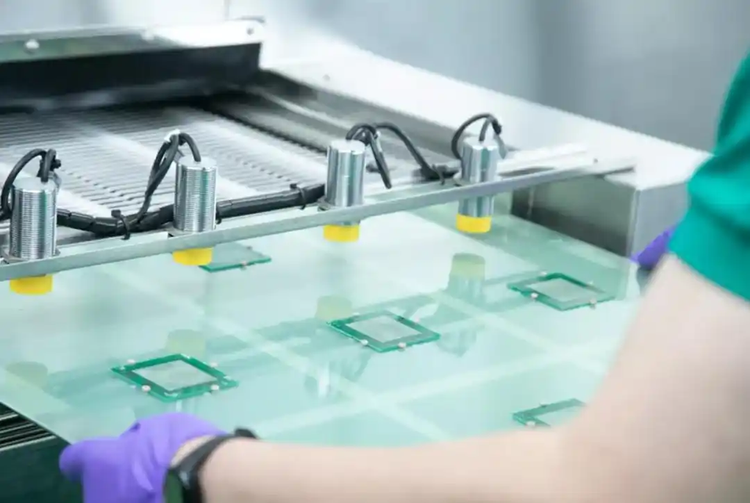
Kao equipped the Hsinchu Fine Cleaning Center with high-spec equipment
Hsinchu is one of the regions with the highest concentration of semiconductor manufacturing companies globally. TSMC's headquarters and its most advanced process R&D and mass production bases are located here. UMC, PSMC, Macronix, Winbond, and other foundries are also rooted here. In packaging and testing, companies like KYEC and Chipbond gather, while substrate players Unimicron and Kinsus have formed complete supply clusters in northern Taiwan.
Choosing this moment to locate its first overseas cleaning center in Hsinchu positions Kao for this wave of AI-driven capacity expansion. Currently, AI chips from companies like NVIDIA and AMD commonly use packaging solutions like CoWoS. TSMC has been continuously expanding advanced packaging capacity in recent years, yet supply still falls short of demand.
The more packaging layers and the more complex the structure, the higher the number and difficulty of cleaning steps. As a consumable used in every key step, the demand for cleaning agents grows in sync with advanced packaging capacity expansion.
In the conference call for the fiscal year 2026 interim report, Kao executives revealed that they plan to continue defending and expanding their back-end share in the future, further penetrating established strongholds like package substrate cleaning. Additionally, they aim to expand from NAND to areas like DRAM and logic semiconductors.
Against the backdrop of businesses like fat and oil chemicals continuously facing raw material price fluctuations, the company has explicitly stated it will shift focus toward electronic materials and semiconductor-related products.
04. Conclusion: Cross-industry semiconductor players win by focusing on the same thing
In semiconductor manufacturing, the monetary proportion of the cleaning segment is far less than that of equipment and main materials, but its impact on yield is direct and rigid. As advanced packaging drives a continuous increase in the number of cleaning steps, the strategic value of such "low-profile, high-stickiness" material businesses is being re-evaluated.
Kao's case is not an isolated example. Ajinomoto's ABF film, TOTO's electrostatic chucks, and Nitto Denko's dicing tapes are all representative products. These Japanese companies' main businesses are MSG, sanitary ware, and tape, respectively, yet each holds a leading position in a niche segment of semiconductor materials.
Their commonality lies in the fact that their underlying technologies stem from long-term accumulation in their main businesses. Competition in semiconductor materials is, to a large extent, competition based on foundational chemical expertise—precisely the part that is difficult to rapidly build.
This article is from the WeChat public account "ChipNews," author: Chen Junda, editor: Xinyuan