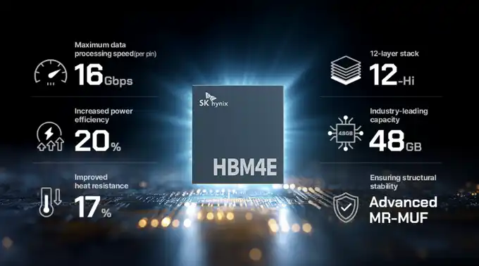
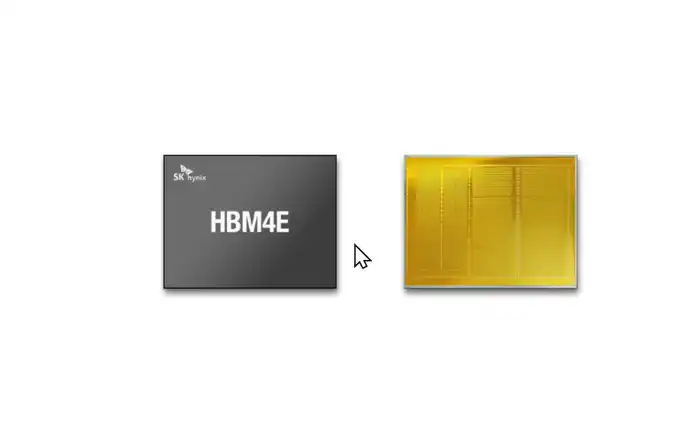
SK Hynix has delivered HBM4E samples to key customers. This flagship 12-layer stacked memory achieves a data transfer speed of 16Gbps per pin, improves power efficiency by over 20%, reduces thermal resistance by 17%, and offers a single-chip capacity of 48GB. Upon the news, the company's stock price surged 7.3% intraday to a record high, fueling market expectations for its continued leadership in the AI memory race.
SK Hynix announced the delivery of samples of its next-generation AI memory chip, HBM4E, to key customers, pushing its stock price to a historic high.
SK Hynix stated on its official website on Thursday that this 12-layer stacked HBM4E product achieves a maximum data processing speed of 16Gbps per pin, improves power efficiency by over 20% compared to the previous generation, and reduces thermal resistance by 17% through advanced packaging technology. SK Hynix indicated it will work closely with partners to achieve timely mass production.
This sample delivery marks SK Hynix's accelerated technological iteration in the high-bandwidth memory field, further solidifying its core position in the AI infrastructure supply chain and providing the market with the latest signal of the company's continued leadership in the HBM technology roadmap.
Following the announcement, SK Hynix's stock price rose 7.3% intraday on the Korean trading platform, reaching a record intraday high. This gain reflects the market's strong anticipation of the company's sustained lead in the AI memory race. From HBM3 and HBM3E to HBM4, SK Hynix has established complete delivery capabilities from mass production to supply. The on-time delivery of these HBM4E samples further strengthens investor confidence in its ability to deliver on its technological promises.
Dual Leap in Performance and Efficiency
SK Hynix disclosed in its statement that the 12-layer HBM4E achieves significant improvements in both performance and power efficiency.
Specifically, the product achieves a maximum data processing speed of 16Gbps per pin, with power efficiency improved by over 20% compared to the previous generation. Additionally, HBM4E effectively reduces data transmission latency through its latest interface design and optimization, while maintaining stable operation in high-bandwidth environments. These features directly enhance data processing capabilities in AI training and inference scenarios, helping customers improve operational efficiency in AI data centers and large-scale computing systems.
Advanced Packaging Technology Enables 48GB Capacity
In terms of packaging process, SK Hynix employs Advanced MR-MUF (Mass Reflow-Molded Underfill) technology to achieve a single-chip capacity of 48GB within a 12-layer stacked structure while ensuring structural stability.
The MR-MUF process protects circuits by injecting liquid protective material between chips. SK Hynix has further optimized this process for HBM4E, reducing its thermal resistance by 17% compared to the previous generation HBM4, thereby ensuring stable operation of the memory chips in high-performance computing environments. This technological breakthrough is particularly critical for AI data centers operating under continuous high loads.
In a statement, Ahn Hyun, President and Chief Development Officer of SK Hynix, said: "SK Hynix, with its market-leading technology capabilities and manufacturing expertise, is laying the groundwork to reinforce its AI leadership based on HBM4E. Through close collaboration with our partners, we will deliver the value the market needs, while further solidifying our technological leadership position as a full-stack AI memory creator."
SK Hynix emphasized that its accumulated experience in the mass production and supply of HBM3, HBM3E, and HBM4 served as an important foundation for the on-time delivery of these HBM4E samples. The company stated it will leverage its market-validated product reliability and supply capabilities to support the development of next-generation infrastructure and help address performance bottlenecks in AI systems.