0.7nm Process Chip Emerges, Moore's Law Lives On

marsbitОпубліковано о 2026-06-26Востаннє оновлено о 2026-06-26

Анотація

IBM has unveiled the world's first sub-1-nanometer (0.7nm) chip technology, integrating nearly 100 billion transistors into an area the size of a fingernail. This breakthrough doubles the transistor density of current 2nm chips and promises a 50% performance gain or a 70% improvement in power efficiency. The achievement is powered by IBM's "NanoStack" architecture, a pioneering 3D design featuring vertically stacked nanosheet transistors. This evolution from FinFET and Gate-All-Around (GAA) technologies offers superior electrostatic control. IBM has demonstrated the technology's viability with functional CMOS inverters and a 40% area reduction in SRAM, crucial for AI chip data bandwidth. Addressing the critical power consumption challenges in AI computing, this advancement extends the roadmap for chip miniaturization. While IBM does not manufacture chips itself, it licenses its process technology to partners. The company projects that NanoStack-based chips could enter production within the next five years, potentially sustaining Moore's Law for another decade.

Is Moore's Law saved?

IBM unveiled the world's first 0.7 nanometer chip process node, integrating nearly 100 billion transistors on a chip the size of a fingernail, achieving a density double that of 2nm chips.

Previously, TSMC's most advanced process was 2nm, which had been difficult to advance beyond for years.

NVIDIA CEO Jensen Huang had repeatedly declared Moore's Law dead, but now there is finally a turning point.
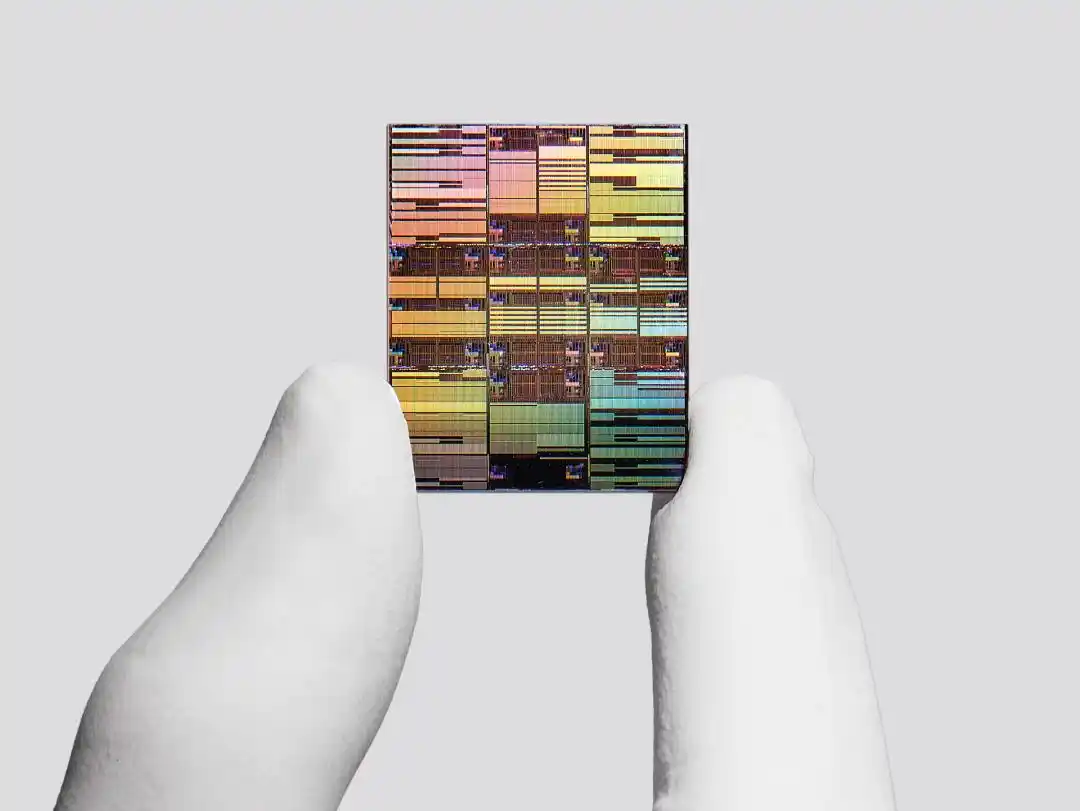
0.7 nanometers, or 7 angstroms, marks the first time human-made transistors have broken through the 1 nanometer threshold, approaching the scale of individual atoms (0.1-0.5 nanometers).

Compared to the 2nm process, it can deliver either a 50% performance improvement or a 70% increase in power efficiency; one or the other.

NanoStack Architecture Arrives

The core of this breakthrough is IBM's "NanoStack" architecture, the industry's first 3D vertically stacked transistor design based on nanosheets.

To understand NanoStack, one must first review the path chip architecture has taken in recent years.

In the 7nm and 10nm era, the mainstream solution was FinFET (Fin Field-Effect Transistor) with the gate wrapping around the channel on three sides to control current. Below 5nm, FinFET's leakage issues became increasingly severe and unsustainable.

In 2017, IBM introduced the Gate-All-Around (GAA) nanosheet technology, where the gate completely surrounds the horizontally stacked nanosheet channel on all four sides, significantly enhancing electrostatic control. This became the technical foundation for its 2nm chip and was subsequently adopted by mainstream manufacturers like TSMC and Samsung.

At the end of 2021, IBM and Samsung jointly announced the VTFET (Vertical-Transport Field-Effect Transistor), which changed the current flow direction from horizontal to vertical. Simulation data showed it could either double performance or reduce power consumption by 85% compared to a similarly sized FinFET solution.

This NanoStack is a further extension of the above roadmap.

Its method is:

Take two wafers with nanosheet transistors, invert one and place it on top of the other, bonding them via an ultrathin dielectric bonding layer to form a vertically interconnected 3D structure. Each layer can use different material combinations, allowing n-type and p-type transistors to be independently optimized without interference.
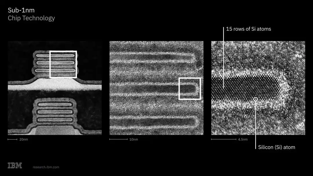
IBM has already completed validation in the lab, demonstrating CMOS integration, dual-channel engineering capabilities, and a fully functional CMOS inverter with switching performance meeting expectations, confirming that this technology can be manufactured and support real computation.

At the VLSI 2026 symposium, IBM further showcased NanoStack's performance on SRAM: a 40% area reduction. SRAM is a core component of on-chip cache, which has long been extremely difficult to scale down. This progress is particularly crucial for the high-bandwidth data pathways required by AI chips.

"Nobody Wants to Pay the Electricity Bill"

Huiming Bu, vice president of chip research at IBM Research, stated: Everyone wants higher performance, but nobody wants to pay the electricity bill.

This is the reality facing the current AI computing power race. The energy consumption of AI chips has evolved from a technical issue to an infrastructure problem, with some data center projects experiencing construction delays due to insufficient power supply.

The 70% power efficiency improvement offered by the 0.7nm technology directly addresses this demand.

However, IBM itself no longer manufactures or sells chips. It develops manufacturing process technologies at its research center in Albany, New York, and then licenses them to chip manufacturers.

Past licensees have included Samsung and the newly formed Japanese semiconductor company Rapidus. Huiming Bu declined to disclose potential customers for the 0.7nm technology.

Regarding competing solutions, the Belgian research institute Imec is advancing another 3D architecture scheme, building transistor structures through layer-by-layer stacking, which has attracted attention from several chip manufacturers.

For mass production, IBM's given timeline is: NanoStack technology could achieve mass production within the next five years at the earliest.

IBM's semiconductor roadmap predicts that with the NanoStack architecture, chip scaling can continue for at least another decade.

References:

[1]https://newsroom.ibm.com/2026-06-25-ibm-debuts-worlds-first-sub-1-nanometer-chip-technology

This article is from the WeChat public account "QbitAI", author: Meng Chen

Трендові криптовалюти

Пов'язані питання

QWhat is the name of the new architecture that enabled IBM's 0.7nm chip breakthrough?

AThe new architecture is called 'NanoStack'. It is the industry's first three-dimensional, vertically stacked transistor design based on nanosheets.

QAccording to the article, what is a key challenge that the improved energy efficiency of the 0.7nm process aims to solve?

AIt aims to address the growing AI compute power consumption, which is evolving from a technical issue into an infrastructure problem. This is because some data center projects face construction delays due to insufficient power supply, and users want higher performance without significantly higher electricity bills.

QHow does IBM's 0.7nm chip compare to a 2nm chip in terms of performance or energy efficiency?

ACompared to a 2nm process, the 0.7nm technology offers a choice: it can provide either a 50% performance improvement or a 70% increase in energy efficiency.

QWhat significant milestone does the 0.7nm (7 Angstrom) transistor represent in semiconductor manufacturing?

AIt represents the first time a human-made transistor has broken the 1-nanometer threshold, bringing its scale close to that of individual atoms (0.1-0.5 nanometers).

QWhat is IBM's estimated timeline for the NanoStack technology to reach mass production?

AIBM's timeline suggests that the NanoStack technology could enter mass production as early as within the next five years.

Пов'язані матеріали

$2 Trillion: Countdown to AI's Largest IPO in History

The countdown for the largest IPO in AI history, a potential $2 trillion listing for Anthropic, is underway for October. The staggering valuation, reportedly projected by several investors, contrasts with the company's own internal restraint on setting a public target. Founded five years ago by former OpenAI core members, Anthropic's growth has been meteoric. Annual recurring revenue (ARR) surged from ~$9B in late 2025 to $47B by May 2026, with Q2 2026 revenue of $11.5B marking a 14x year-over-year increase. Bank valuations are even based on internal 2028 revenue forecasts of $190-200B. A key growth driver is Claude Code, its AI coding assistant. Its ARR quintupled in five months to $2.5B by February 2026, now constituting nearly 20% of total revenue. Surveys indicate Anthropic commands roughly 40% of enterprise LLM spending, doubling OpenAI's share in programming-specific use. However, alongside this explosive growth, reports detail significant internal cultural strife. Critics describe a divisive "priesthood" of PhD executives, led by CEO Dario Amodei, who promote a "save humanity" narrative that some employees find cult-like and alienating. This has reportedly created a demoralized workforce and a covert "underground network" of dissent among engineers torn between lucrative pre-IPO equity and a toxic work environment. Anthropic now faces a pivotal paradox: pursuing its mission of "safe" AI requires immense capital for compute, yet that capital demands relentless commercial growth. As it approaches its historic IPO, the company must navigate intense regulatory scrutiny, soaring operational costs, and internal tensions—any of which could destabilize its post-listing trajectory, much like SpaceX's significant post-IPO stock drop. The stage is set for a defining moment in tech history.

marsbit2 хв тому

$2 Trillion: Countdown to AI's Largest IPO in History

marsbit2 хв тому

AI Boosting Efficiency and Cutting Costs Makes VC Increasingly Expensive

"AI for Cost Reduction Makes VC Funding More Expensive" Despite the "cost-reduction and efficiency" narrative of AI, venture capital (VC) investment in the AI sector is becoming increasingly costly. While AI tools lower the initial costs for many startups—with team sizes shrinking across funding stages—the market is polarizing. For top-tier AI teams, especially those from leading companies like Google and OpenAI, funding rounds are now larger and valuations are higher than ever at the seed and early stages. For example, new ventures by prominent researchers are securing billions in funding with valuations reaching tens of billions before having a mature product. This creates a "barbell" market: lightweight startups need less capital, while elite AI firms attract massive investments early on. This dynamic raises the cost for VCs to acquire and maintain meaningful ownership stakes. As valuations soar early, securing the same equity percentage requires significantly larger capital commitments. VCs must now invest more upfront and reserve substantial funds for follow-on rounds to avoid dilution, prompting large firms like Accel and a16z to raise massive new funds. Consequently, capital is concentrating intensely in a few perceived winners like OpenAI and Anthropic, widening the gap between large and small VC funds. While high valuations bake in future growth expectations, they also compress potential returns, demanding that portfolio companies achieve unprecedented scale. For major VCs, the core strategy is clear: secure early positions in potential winners and maintain the capital to keep investing as valuations rapidly escalate.

marsbit28 хв тому

AI Boosting Efficiency and Cutting Costs Makes VC Increasingly Expensive

marsbit28 хв тому

An Eight-Year Investment Takes a Sharp Turn: Why Did Ethereum Suddenly Abandon Poseidon?

On August 13, Ethereum researcher Justin Drake announced a significant shift in Ethereum's Layer-1 cryptographic roadmap: abandoning the SNARK-friendly hash function Poseidon in favor of traditional functions like SHA2 or BLAKE2. This decision ends eight years of research and investment, marking a major revision to the post-quantum security strategy. Poseidon, introduced in 2019, was highly efficient for zkRollups and zkVMs within SNARK circuits. However, its need for prolonged cryptanalysis and the pressing timeline for quantum resistance revealed limitations. Recent breakthroughs in SNARK design, specifically using binary fields, now enable traditional, battle-tested hash functions to perform as efficiently as Poseidon within SNARKs. Benchmarks show modern laptops can now verify over a million traditional hash calls per second. This change is partly driven by accelerated concerns over quantum computing threats. Reports warn that "Cryptographically Relevant Quantum Computers" could break current blockchain signatures like ECDSA by the early 2030s, risking trillions in assets. Ethereum's response focuses on hash-based post-quantum signature schemes, deemed more quantum-resistant than some lattice-based alternatives under pressure from AI cryptanalysis. Ethereum's updated post-quantum roadmap targets a production-ready "leanVM" for signature aggregation by 2027, with full deployment across consensus, execution, and data layers by 2028. The shift to mature hash functions like SHA2 reduces reliance on newer algorithms and aligns with the goal of using widely analyzed cryptographic primitives. Other major blockchains are also preparing. Solana's core teams have independently chosen the NIST-standardized Falcon signature scheme for its compact size. Starknet plans a phased migration, starting with replacing its Pedersen hash with BLAKE2. Ethereum's move signifies a strategic pivot towards proven security foundations for the quantum era.

marsbit1 год тому

An Eight-Year Investment Takes a Sharp Turn: Why Did Ethereum Suddenly Abandon Poseidon?

marsbit1 год тому

Programmers Worldwide Are Wasting Money on Anthropic! The Company Can't Stand It Anymore

Anthropic recently published guidelines to help developers using Claude Code reduce unnecessary token costs. The key recommendations include: 1) Clear (/clear) conversations after completing a task to avoid carrying irrelevant file reads and command outputs into the next task. 2) Set the model and reasoning effort level at the start of a session, as switching mid-session invalidates the prompt cache, requiring a full-price recalculation of the entire dialog history. 3) Attach files using @ references instead of typing paths manually to avoid extra tool calls and searches that bloat the context. 4) Add quiet flags to verbose commands (e.g., in CLAUDE.md) to minimize lengthy output in the dialog history. 5) Use /compact while the session cache is still warm (before breaks) to compress the dialog at one-tenth the cost. 6) Offload large-output tasks to a sub-agent, which runs in an isolated context and only returns conclusions, preventing intermediate outputs from polluting the main dialog. The article explains token pricing: input tokens (prefill) are processed in parallel, while output tokens (decode) are generated serially, making output tokens five times more expensive. Caching is crucial for savings—if a request's prefix (system prompt, CLAUDE.md, dialog history) matches the previous one byte-for-byte, reading it costs only 10% of the standard input price. However, cache invalidation occurs when changing models, effort levels, fast mode, compressing dialogs, after cache expiration, or when resuming old sessions. Dialog history also grows quadratically (O(n²)) as file contents and command outputs accumulate, increasing costs per round. Proactive context management—like isolating noisy tasks, using /rewind to trim unproductive turns, and task-based session clearing—is becoming an essential skill for cost-effective AI-assisted development.

marsbit3 год тому

Programmers Worldwide Are Wasting Money on Anthropic! The Company Can't Stand It Anymore

marsbit3 год тому

Pax Silica vs. WAICO: The US Wants to Prohibit Europe from Using Chinese Artificial Intelligence

The United States is preparing to demand that European and other partners abandon Chinese artificial intelligence initiatives, threatening exclusion from the American-led "Pax Silica" coalition, according to a leaked U.S. State Department document. This ultimatum forces signatories of the "AI Opportunity Statement" to choose between the Western technological ecosystem and alternative frameworks, with China not explicitly named but clearly targeted. Pax Silica is a U.S. strategy for AI and semiconductor hegemony, launched in late 2025. Its European presence expanded significantly in mid-2026. Concurrently, China, Russia, and 27 other nations established the World AI Cooperation Organization (WAICO) in July 2026 as an independent intergovernmental platform promoting AI governance based on UN principles. This situation creates a difficult choice, especially for European nations balancing strategic autonomy with dependence on U.S. tech and security. It also pressures Global South countries with pragmatic ties to both Washington and Beijing. The formation of competing blocks risks fragmenting the global tech landscape, forcing companies to split supply chains, increasing costs, and potentially leading to incompatible standards and protocols. The era of open globalization in AI may be ending, replaced by geopolitical confrontation where technological sovereignty trumps economic efficiency. The decisions made will shape the global digital economy for decades.

cryptonews.ru5 год тому

Pax Silica vs. WAICO: The US Wants to Prohibit Europe from Using Chinese Artificial Intelligence

cryptonews.ru5 год тому

Торгівля

Спот

Популярні статті

Як купити CHIP

Ласкаво просимо до HTX.com! Ми зробили покупку USD.AI (CHIP) простою та зручною. Дотримуйтесь нашої покрокової інструкції, щоб розпочати свою криптовалютну подорож.Крок 1: Створіть обліковий запис на HTXВикористовуйте свою електронну пошту або номер телефону, щоб зареєструвати обліковий запис на HTX безплатно. Пройдіть безпроблемну реєстрацію й отримайте доступ до всіх функцій.ЗареєструватисьКрок 2: Перейдіть до розділу Купити крипту і виберіть спосіб оплатиКредитна/дебетова картка: використовуйте вашу картку Visa або Mastercard, щоб миттєво купити USD.AI (CHIP).Баланс: використовуйте кошти з балансу вашого рахунку HTX для безперешкодної торгівлі.Треті особи: ми додали популярні способи оплати, такі як Google Pay та Apple Pay, щоб підвищити зручність.P2P: Торгуйте безпосередньо з іншими користувачами на HTX.Позабіржова торгівля (OTC): ми пропонуємо індивідуальні послуги та конкурентні обмінні курси для трейдерів.Крок 3: Зберігайте свої USD.AI (CHIP)Після придбання USD.AI (CHIP) збережіть його у своєму обліковому записі на HTX. Крім того, ви можете відправити його в інше місце за допомогою блокчейн-переказу або використовувати його для торгівлі іншими криптовалютами.Крок 4: Торгівля USD.AI (CHIP)Легко торгуйте USD.AI (CHIP) на спотовому ринку HTX. Просто увійдіть до свого облікового запису, виберіть торгову пару, укладайте угоди та спостерігайте за ними в режимі реального часу. Ми пропонуємо зручний досвід як для початківців, так і для досвідчених трейдерів.

832 переглядів усьогоОпубліковано 2026.04.21Оновлено 2026.06.02

Як купити CHIP

Обговорення

Ласкаво просимо до спільноти HTX. Тут ви можете бути в курсі останніх подій розвитку платформи та отримати доступ до професійної ринкової інформації. Нижче представлені думки користувачів щодо ціни CHIP (CHIP).

活动图片