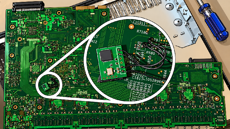
A blogger released information suggesting that, based on messages from TeraFab, Elon Musk appears to be pursuing the FEL (Free Electron Laser) route to disrupt the monopoly of traditional EUV.
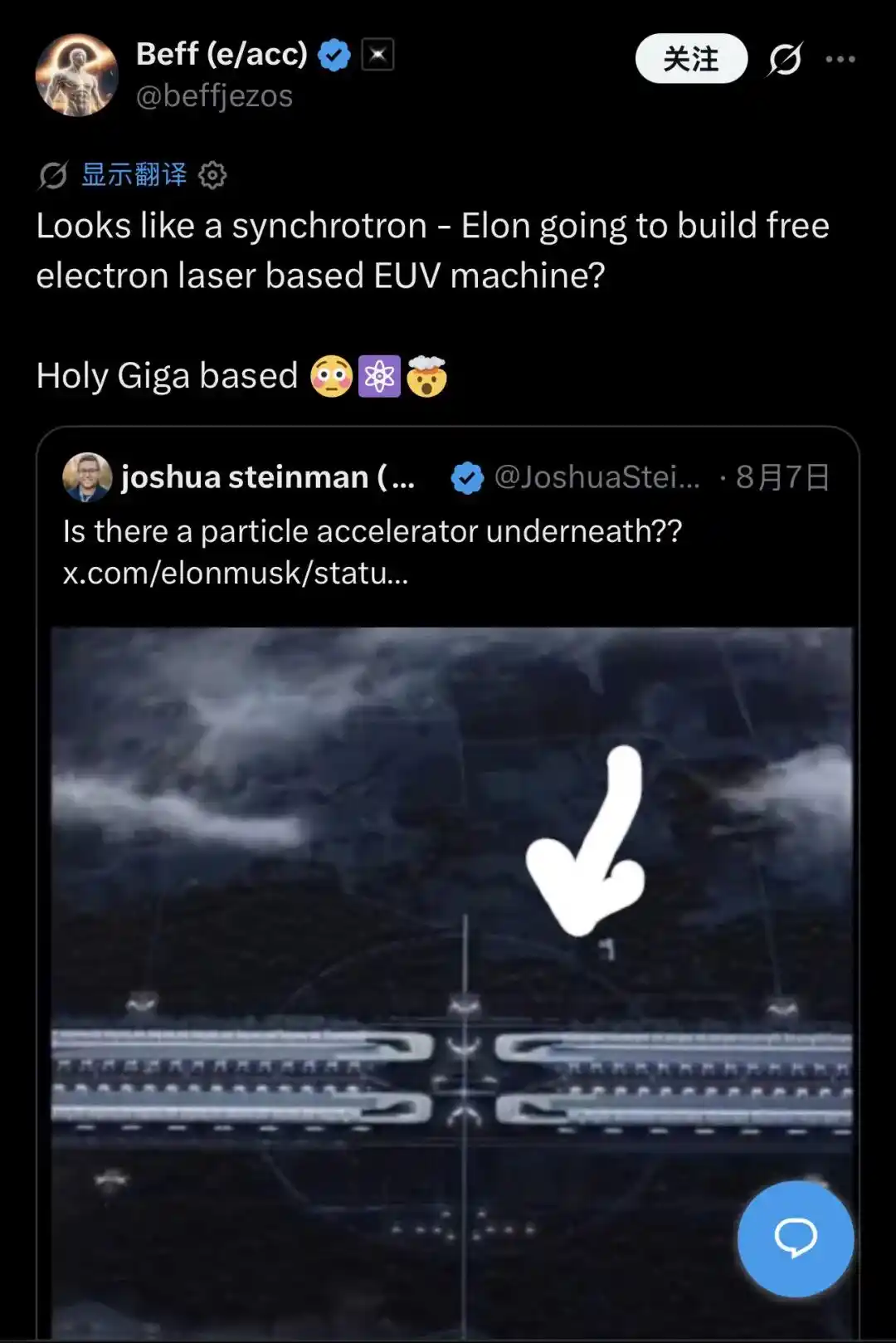
Subsequently, Elon Musk's reply seemed to confirm this speculation.
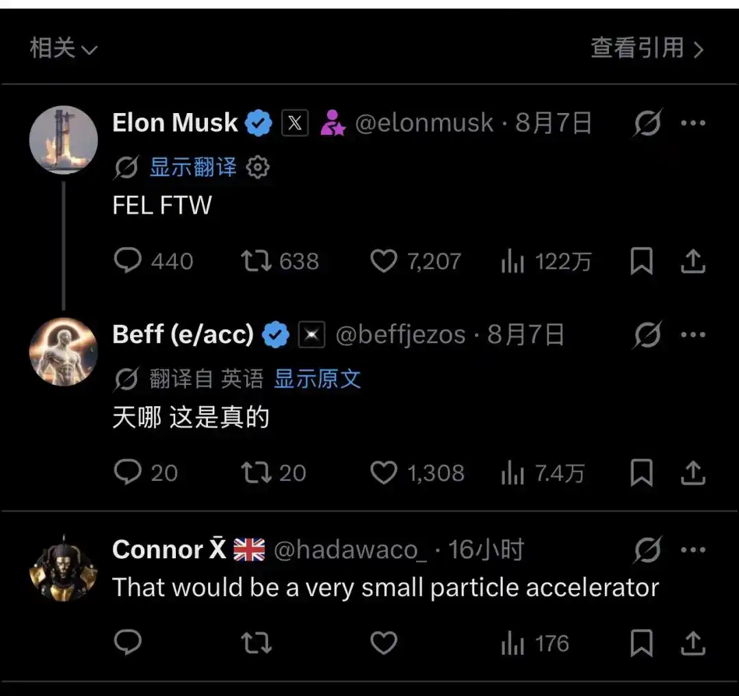
Of course, this is a conjecture and does not represent reality. But we believe it's worth discussing.
FEL, Not a New Thing
We must acknowledge that Free Electron Lasers (FELs) and particle accelerators are not new. For years, companies, R&D institutions, and universities have owned and operated particle accelerators to generate tiny subatomic particles like protons, neutrons, and quarks. These systems are typically used for physics and other scientific applications. Free Electron Lasers (FELs) have long existed. As introduced, this is essentially a high-power light source that uses electrons to generate light of different wavelengths. A particle accelerator is a system that propels charged particles.
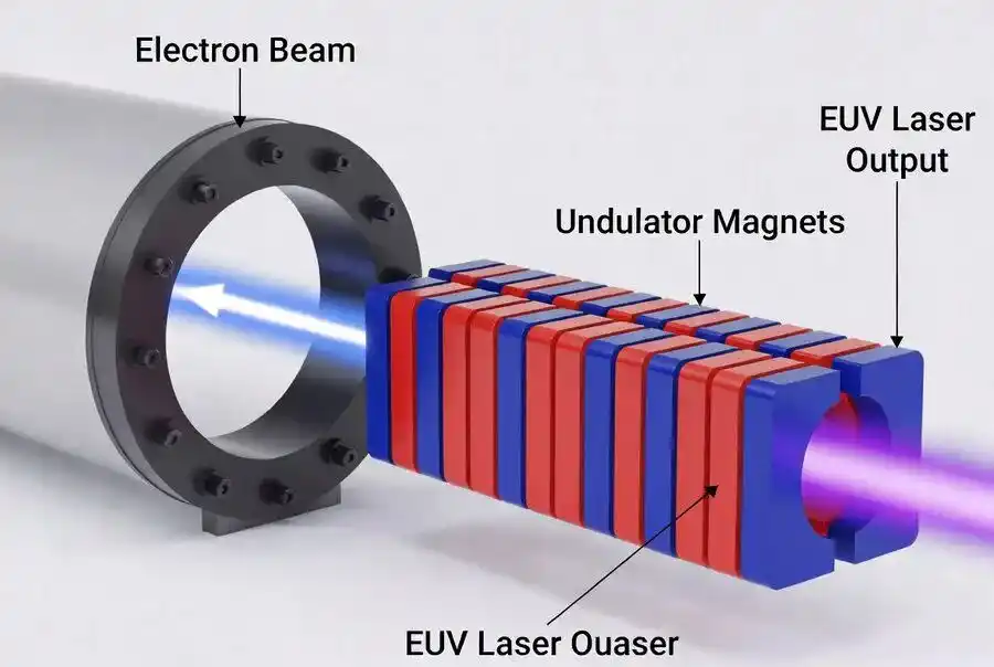
In principle, a Free Electron Laser is generated by electrons flying at near-light speed passing through a periodically varying magnetic field. The wavelength of this laser is related to the frequency of the periodic magnetic field's process; by changing the frequency of the magnetic field variation or the incident speed, different wavelengths of laser light can be obtained. So, to make this FEL, one first needs a high-speed (near-light speed) electron source. Why electrons near light speed? Because only under such conditions can the radiation light generated by the electron's oscillation perpendicular to the incident direction significantly affect the electron's motion, causing adjacent electrons to cluster together (rather than forming a uniform electron beam).
Assuming each cluster has N electrons, the superimposed energy of their radiation is not a simple sum of the energies of N electrons but is related to the square of N, meaning the radiation resonates—in other words, it becomes laser light. Currently, linear accelerators are most commonly used as high-speed electron sources (although synchrotron radiation is also used as a free electron source, its power is insufficient).
In other words, in an FEL, electrons move freely in a vacuum at near-light speed and exchange energy with a co-propagating electromagnetic wave, thereby producing a tunable, exponentially amplified light beam.
Specifically, it includes the following parts:
1. High-Energy Electron Beam
This process begins with a high-energy electron beam from a particle accelerator.
A microwave amplifier accelerates electrons to near-light speed. Taking a 1 GeV electron beam (i.e., one electron charge multiplied by 1 gigavolt) as an example, the electron's speed is only one ten-millionth slower than light. The higher the energy of the electron beam, the higher the photon energy the FEL can produce.
2. Radiation from Accelerated Charges
Any accelerated charged particle radiates light. For example:
Bremsstrahlung (German for "braking radiation") light sources work by colliding electrons into a metal wall, causing them to decelerate rapidly; the electron beam dissipates energy by radiating light and releasing heat.
Deflecting magnets can achieve a similar effect:
If the electron beam is bent into a circular orbit, you get a synchrotron radiation source.
If the electron beam is made to oscillate back and forth along a sinusoidal trajectory, it forms a wiggler or undulator light source.
Synchrotron radiation and wiggler sources produce light with a broad frequency range, while undulators are different: under specific conditions, an electron beam passing through an undulator can achieve laser emission.
3. Undulator
An undulator is a device composed of periodically arranged magnets that cause a high-energy electron beam to oscillate along a sinusoidal curve (i.e., "wiggle") at a specific frequency. This controlled oscillation of the electron beam is the first step in producing precisely tuned light. The undulator's period (λu) and the electron beam energy together determine the wavelength of the output light.
Because of this, some see FEL as a potential replacement for EUV lithography.
A Candidate to Replace Current Light Sources
Traditional EUV lithography uses 13.5 nm because tin plasma can relatively efficiently generate light in this wavelength band.
But the logic of FEL is completely different. By adjusting electron beam energy, undulator period, and magnetic field strength, the output light wavelength can be changed. Therefore, in theory, it can cover from soft X-rays, EUV, to longer wavelengths. This means: traditional EUV is more like a "lithography knife" with a fixed focal length, while FEL is more like an "optical tool" that can continuously adjust its wavelength.
Thus, some are using FEL to break through limitations. The US startup xLight is a proponent of this path. It's worth noting that former Intel CEO Pat Gelsinger now serves as Executive Chairman of xLight.
In xLight's technology, electrons are first injected into a particle accelerator, then enter the Free Electron Laser (FEL). xLight states: "The FEL utilizes electrons from the particle accelerator and passes them through an undulator with a periodic magnetic field, thereby producing a coherent, high-intensity light beam."
Simply put, EUV light is generated in the accelerator. Then, the EUV light is transmitted from the particle accelerator facility to the fab through a photon-pipeline-like device. At this point, the EUV light is directed to a sub-fab. Inside the sub-fab are various independent systems called "turnaround stations."
According to xLight's video, each turnaround station is dedicated to one EUV tool in the upper-level fab. During operation, EUV light is transmitted to each turn station in the sub-fab area. Then, each turn station receives the light and directs it to the EUV system upstairs in the fab. This, in turn, powers the EUV equipment.
In this scenario, the EUV lithography equipment itself does not contain an LPP light source. Instead, EUV light is generated in a particle accelerator and then transmitted to the fab's EUV equipment. This is a simplified way to describe a complex process.
Nonetheless, xLight's FEL light source produces power 4 times higher than current LPP setups. xLight claims: "By delivering up to 4x more EUV power, fabs can optimize pattern improvement, increase productivity and yield, thereby generating additional billions of dollars in revenue per scanner annually and reducing cost per wafer by about 50%. Furthermore, a single xLight system can support up to 20 ASML systems, with a lifespan of up to 30 years, thereby lowering capital and operational expenditures by more than 3 times."
In theory, xLight's technology could be used for low numerical aperture EUV, high numerical aperture EUV, and even hyper numerical aperture EUV. In R&D, ASML is developing 0.75 hyper numerical aperture EUV technology, targeting a more distant future.
Judging from Terafab's elongated factory design and Musk's reply, it's highly likely that Terafab might adopt a linear accelerator as the high-speed electron source for FEL. Currently, femtosecond-level free-electron X-ray lasers are already used in university laboratories for protein crystal diffraction data collection.
If you still don't understand how powerful this thing is, here's an analogy: if AMSL's extreme ultraviolet lithography machine's light source is an ordinary light bulb, then the FEL free-electron extreme ultraviolet light source is equivalent to a high-efficiency laser, easily capable of producing laser output power ranging from several kilowatts to tens of kilowatts, with a wavelength that can be arbitrarily adjusted.
In comparison, ASML's LPP EUV has a fixed wavelength, and its power is difficult to exceed 1 kilowatt. Moreover, both the purity of the light wavelength and its coherence are incomparable. If it can be successfully developed, it will greatly accelerate the lithography speed and quality of lithography machines. FEL also has another advantage: its conversion efficiency (energy consumption ratio) is particularly high. ASML's LPP requires about 4.4 MW of electricity to produce 1 kW of usable EUV (overall efficiency around 0.05%).
In contrast, the most advanced Energy Recovery Linac FEL (ERL-FEL) requires only about 0.7 MW of electricity to produce 1 kW of EUV, which is 6 times more efficient. Future use of better superconducting materials could further improve this.
Can't Be Achieved Overnight
Looking solely at the technology itself, FEL clearly has superior light source performance, but it doesn't necessarily mean it's more advanced for industrial lithography. Because EUV lithography requires more than just "having a beam of 13.5 nm light."
It also needs: high power + high stability + high repetition frequency + high reliability + extremely low cost + extremely high uptime + compatibility with reflective optical systems.
ASML's current EUV light source, after years of engineering, has formed a complete industrial system.
In contrast, FEL typically requires large-scale electron accelerators, undulators, vacuum systems, beam control systems, etc., making the equipment volume and cost very substantial. So, if viewed from the perspective of light source physical performance: FEL is clearly stronger and more flexible.
But from the perspective of engineering capability for semiconductor mass-production lithography: the mature EUV light source is currently more suitable for fabs. FEL has the potential to shift the EUV light source from the "fixed wavelength of 13.5 nm" towards more flexible short-wavelength lithography.
For example, in the future, if exploration moves into next-generation lithography at 6.x nm, 5.x nm, or even shorter wavelengths, the light source mechanism of FEL—with its tunable wavelength, high coherence, and high peak brightness—would become very attractive.
But here lies a huge problem: the shorter the wavelength, the more difficult the issues with optical systems, masks, photoresists, reflectivity, photon scattering, vacuum systems, etc., become.
Therefore, the real revolution FEL might bring is not just "replacing the EUV light source," but rather providing a completely different route for short-wavelength, high-brightness light sources.
Apart from FEL, other discussed solutions include High-Harmonic Generation (HHG), Discharge Produced Plasma (DPP), and synchrotron radiation. LPP wins in maturity and mass production, FEL emphasizes high brightness, high coherence, and wavelength tunability, while HHG has the potential for miniaturization. The key to future competition lies in balancing power, efficiency, stability, and cost at even shorter wavelengths.
More importantly, they all face more challenges, and the timeline is far from certain.
This article is from WeChat public account "Semiconductor Industry Observation" (ID: icbank), author: Editorial Department