In 2026, the global development of AI reached a landmark inflection point—the capital expenditure on inference by hyperscale cloud vendors historically exceeded that on training for the first time. The industry's anchor shifted from 'training large models' to 'using large models,' fundamentally flipping the structure of computing demand.
In the training era, the core challenge of computing power was 'double-precision floating-point and cluster scale'; entering the inference era, the core challenge became 'memory bandwidth and communication latency.'
The bottleneck for large model inference is no longer merely computation, but data movement—model weights, intermediate activations, and KV Cache need frequent interaction between off-chip DRAM (like HBM) and GPUs. The larger the model, the higher the energy consumption and latency of data transfer, ultimately far exceeding the energy consumption of computation itself, thus forming the memory wall.
NVIDIA GPUs have built a solid fortress with CUDA and NVLink, but still cannot avoid GPU idling caused by bandwidth bottlenecks.
A domestic large model company, Zhipu, conducted a simple experiment: In a 512-card inference cluster, keeping the GPUs, model, and code unchanged, but only upgrading the network bandwidth cap from 200GB/s to 400GB/s, inference throughput directly increased by 10%, and first-token output latency decreased by 19%—the principle is simple: widen the road, and the cars can run faster.
However, non-GPU architectures represented by Cerebras seem to be tearing an opening in this memory wall.
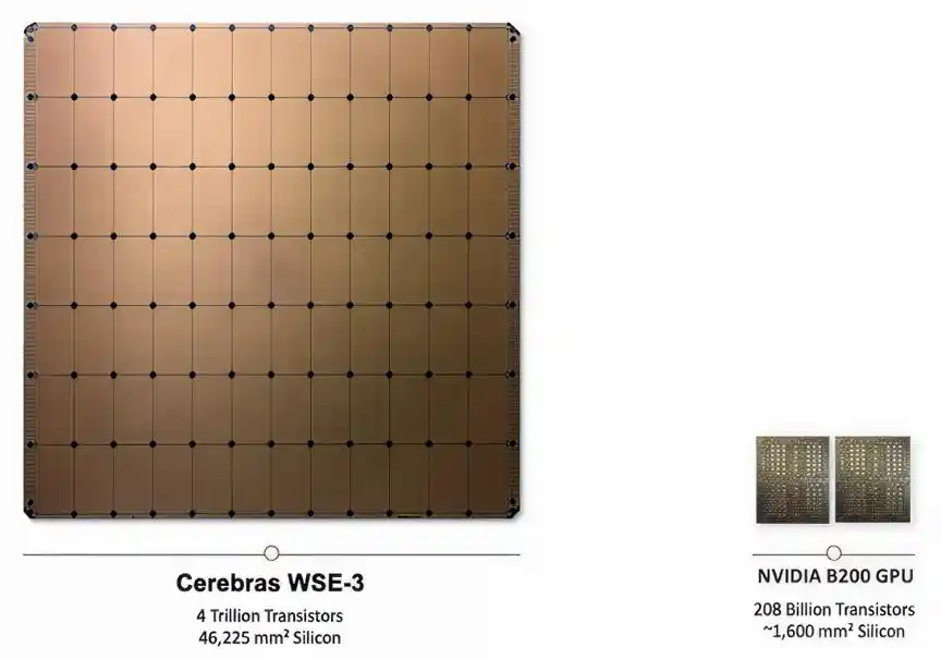
Size comparison between Cerebras WSE-3 chip and NVIDIA B200 GPU
The Essence of Cerebras: A Near-Memory Computer Based on SRAM
Cerebras Systems was founded in Silicon Valley by Andrew Feldman and others. The early founding team all came from SeaMicro, a low-power microserver company that was later acquired by AMD. Subsequently:
In 2015, the founding team established the 'wafer-scale computing' route.
In 2016, they completed registration and Series A financing, entering a stealth R&D phase.
In 2019, they released their first product, the WSE-1 chip and CS-1 system, based on TSMC's 16nm process.
In 2021, they released the second-generation product, based on TSMC's 7nm process.
In 2024, they released the third-generation product (WSE-3 / CS-3), based on TSMC's 5nm process. Both the chip and system are manufactured entirely in the USA, making it a genuinely pure US-made chip system.
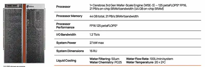
CS-3 system configuration, containing 1 WSE-3 chip
Cerebras's Wafer-Scale Engine (WSE) architecture philosophy is simple, direct, yet hits the pain point: trade extreme physical expansion for extreme compression of data movement latency.
Ordinary chips slice a wafer into many small chips; NVIDIA GPUs follow this approach. Cerebras does the opposite: don't slice, directly turn nearly the entire wafer into one giant chip, called the Wafer-Scale Engine (WSE).
Traditional chips are formed by cutting a 300mm diameter wafer into hundreds of small chips; Cerebras chooses to keep the entire wafer intact, using it directly as the whole chip. The latest WSE-3 boasts 4 trillion transistors, 900,000 AI cores, each equipped with 48KB of local SRAM, giving the entire chip 44GB of on-chip SRAM, providing 21 PB/s of on-chip memory bandwidth and 214 Pb/s of fabric bandwidth—thousands of times the bandwidth of traditional HBM.
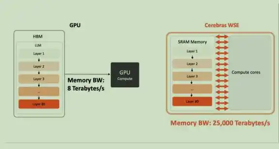
Cerebras WSE's memory bandwidth is 2625 times that of NVIDIA's B200 packaged chip, breaking the memory bandwidth bottleneck in large model inference scenarios.
In Cerebras's architecture, model weights are never stored on the SRAM but reside in off-chip storage (MemoryX) and are transferred layer by layer to the giant chip. The approach involves separating the storage of neural network model weights from the computing units.
All model weights are stored externally in the MemoryX memory extension module. The weights required for computing each layer of the network are transmitted layer by layer to the CS-3 system on demand. Weights are stored in the DRAM and flash memory of MemoryX and transmitted to the CS-3 system at full bandwidth rates. These weights are not stored in the CS-3 system—not even temporarily cached—CS-3 relies on the core's underlying dataflow mechanism to complete computations.
Leveraging its wafer-scale architecture, Cerebras demonstrates barrier-breaking advantages in LLM inference constrained by memory bandwidth. When generating tokens sequentially, weights are streamed layer by layer from off-chip MemoryX to CS-3. For different models, the token rate is 1.5 to 5 times that of NVIDIA's B200.
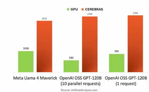
NVIDIA DGX B200 GPU versus Cerebras CS-3 chip, token rate comparison when running different large models
Its core advantage lies in: The 44GB of on-chip SRAM in CS-3 provides 21 PB/s of ultra-high bandwidth (2625 times that of B200) and 214 Pb/s of interconnect bandwidth, freeing weight streaming from HBM interface limitations. Therefore, it performs exceptionally well in TTFT (Time To First Token), long-context, and agent workload scenarios.
Although weights are external to MemoryX, loaded layer by layer on demand, and not cached on-chip, CS-3 relies on the core's dataflow mechanism to perform lossless full FP16 precision computations in SRAM; leveraging linear performance scaling, it also unleashes astonishing total throughput in multi-user concurrent inference.
Besides bandwidth, there is also a power advantage. Recently, in a speech, Sutong Liu, Chairman of InnoLight, mentioned that customers' requirement for optical modules is 1 pJ/bit, while the current level is 10 pJ/bit. In Cerebras chips, the interconnect power consumption is only 0.15 pJ/bit, whereas the current GPU interconnect power consumption is 10 pJ/bit.
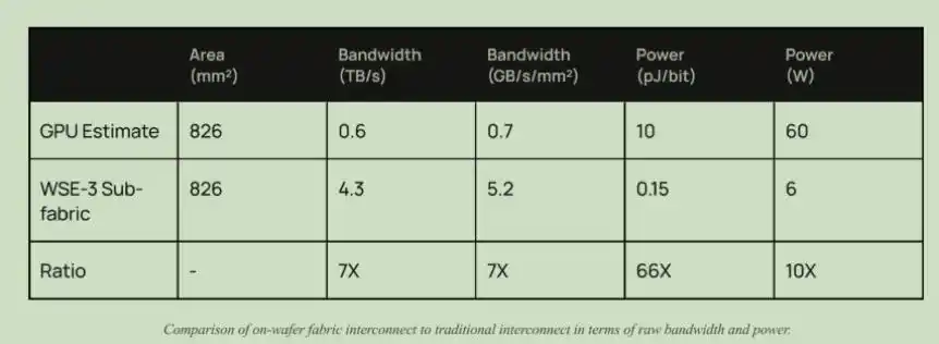
Bandwidth and power consumption comparison between Cerebras interconnect and GPU interconnect architectures
Thus, if Cerebras's wafer-scale large-chip architecture becomes mainstream for AI inference or even training, it might significantly suppress and structurally alter the shipment volumes of traditional optical modules and CPO (Co-Packaged Optics). The core logic is: the high demand for optical modules and CPO essentially aims to solve the bandwidth bottleneck of 'chip-to-chip interconnect' and 'node-to-node interconnect' in GPU clusters; Cerebras's architecture precisely solves the problem by 'eliminating distributed interconnects.'
Counterintuitive: The 'True and False' Fatal Flaws of Wafer-Scale Large Chips
The core of chips always lies in Trade-Off. To achieve extreme on-chip SRAM bandwidth, Cerebras also brings some issues.
Low Yield?
Quite the opposite. The size of a single AI core is reduced to 0.05 square millimeters (1% the size of a single H100 compute core), resulting in higher yield. By routing on-chip, defective cores can be disabled and bypassed, improving defect tolerance by 100 times compared to traditional multi-core processors. The chip actually has 1 million AI cores, but considering yield, it is advertised as having 900,000 AI cores.
Only Good at Inference, Not at Training?
In the years following Cerebras's founding, training was the mainstream topic, so the company focused heavily on training. It's only after inference demand surged that people realized its advantages in inference were more pronounced.
In reality, simplified distributed computing also brings advantages like reduced code complexity and lower communication overhead.
Training a 175-billion-parameter model on 4000 GPUs typically requires about 20,000 lines of distributed training code.
Cerebras achieves equivalent training with 565 lines of code—the entire model can be placed on the wafer without dealing with data parallelism complexity.
SRAM Scaling is Dead; Core Advantage Faces a Physical Ceiling.
The third-generation product is based on TSMC's 5nm, and its SRAM capacity only increased by 10% compared to the second-generation product based on TSMC's 7nm. Beyond 5nm, SRAM cell area hardly shrinks with process node advancement.
This means Cerebras can no longer significantly increase its core advantage (SRAM capacity) by upgrading TSMC's process nodes (e.g., from 5nm to 3nm) as it did before.
Limited by wafer size, cooling capability, and manufacturing costs, on-chip storage resources like SRAM are difficult to scale linearly with computing cores, encountering a resource ratio bottleneck. This almost blocks its evolutionary path.
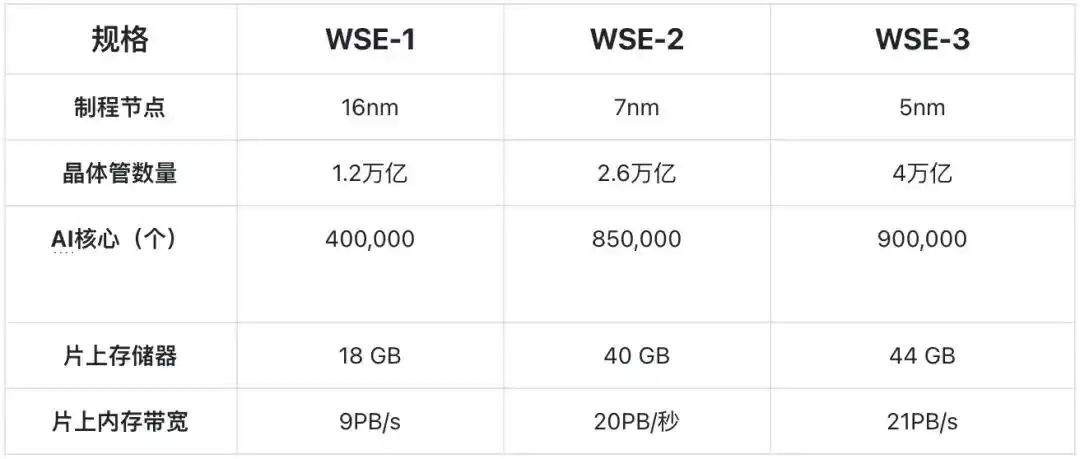
Technical specifications of Cerebras's three product generations
The Triple Purgatory: Cooling, Process, and Ecosystem.
The entire wafer concentrates heat, leading to high heat flux density, necessitating reliance on customized data centers and dedicated liquid cooling systems. Moreover, ecosystem compatibility means customers must adapt to its customized software stack, with weak compatibility with existing general-purpose programming frameworks like CUDA, leading to high software porting and adaptation costs.
Low Off-Chip Bandwidth Creates an Expansion 'Island'.
Due to the limitations of wafer-scale physical design, the number of I/O pins that can be led out from the edge of the WSE is extremely limited, resulting in an I/O bandwidth of only 150GB/s. Compared to NVIDIA NVLink's 1.8TB/s bi-directional bandwidth, it's like a snail. This makes it extremely difficult for WSE to scale out at high speeds. Although Cerebras's SwarmX interconnect performs decently in multi-system combinations, in the face of super-large models requiring high-speed multi-chip interconnection, the extremely low off-chip bandwidth becomes a structural physical shackle.
Route Competition: Big Tech In-House Development—How Much Window Does Cerebras Have Left?
Big tech companies have multiple parallel paths to address 'inference requiring higher bandwidth + lower latency,' not just wafer-scale. They are encircling and suppressing the technological dividends of startups like Cerebras through three concurrent approaches.
1 In-House ASIC Development
Google TPU v8 has already split into training-specific and inference-specific versions; AWS Trainium 4 is on the way; Microsoft Maia is already in use within Azure, built on TSMC's 3nm process, with native FP8/FP4 tensor cores, a redesigned memory system equipped with 216GB HBM3e, and 272MB on-chip SRAM; even Anthropic has begun evaluating in-house inference chip development.
This path is highly probable and will directly cause the TAM (Total Addressable Market) for 'third-party inference procurement' in 2028 to be compressed by 10% to 25%.
2 Process Generalization of the Standard Packaging Route
This is the most direct dimensional reduction attack on Cerebras.
TSMC's SoW (System-on-Wafer) is already widely open to customers, and CoWoS 9.5x interposer will launch in 2027.
What these two products do—stitching multiple dies at the wafer level—essentially makes Cerebras's physical process generic and accessible to all.
NVIDIA's Vera Rubin will enter this ecosystem in the second half of 2026.
Although Cerebras's own cross-reticle stitching is exclusive, the exclusivity window lasts at most 2 to 3 years. Beyond 2027-2028, its process barrier will be diluted by TSMC's advanced packaging.
3 Breakthrough of Optical Interconnect/Optical Computing
The interconnect and memory wall of electronic chips have reached their limits. Photonics' high bandwidth, low latency, and zero crosstalk are the ultimate solution.
Optical routes represented by Lumentum are rising. The biggest advantage of wafer-scale is on-chip computing, but models will inevitably grow larger, making high-speed interconnect beyond wafer scale a necessity.
With the maturity of CPO (Co-Packaged Optics) and Optical Interconnects, it's highly likely we will see optical I/O directly introduced into WSE wafers, breaking the shackles of electrical interconnect. NVIDIA might also acquire companies with specific architectural advantages like LPU (e.g., Groq), combine them with optical interconnects, and develop wafer-scale systems compatible with existing NV super-node software.
Sprinting on the Cliff: Cerebras's Business and Delivery
Cerebras is currently facing a cliff-edge sprint forced by massive orders.
Deals with leading clients like OpenAI are forcing Cerebras to transform from a chip company into a new type of cloud service provider. It no longer just sells hardware but needs to lock in and build massive data center power and facilities in the short term.
According to contract requirements, Cerebras needs to deliver 250MW of data center capacity annually from 2026 to 2028. However, wafer-scale systems have extremely high requirements for data center rooms and cannot be directly placed into traditional air-cooled IDCs. Currently, Cerebras's progress in preparing data center capacity is significantly behind the contract requirements.
From tape-out to factory construction, from power approval to cooling system deployment—this is a quagmire of heavy assets and long cycles.
Epilogue: Left or Right?
Returning to the initial proposition, as the inflection point for inference computing power has arrived, the core of computing architecture always lies in trade-offs.
There is no absolute right or wrong, only the relatively optimal solution for the most important workloads. And workloads are already changing.
Cerebras goes left, choosing extreme physical optimization, trading the entire wafer and massive SRAM for extreme low latency for a single task, which is unbeatable in scenarios extremely sensitive to first-token latency.
NVIDIA goes right, choosing to maintain generality, using HBM + NVLink + massive cluster throughput to handle ever-changing workloads, responding with constancy to change.
The winds are shifting, and the road ahead is uncertain. It is precisely this dual uncertainty of technology and business that breeds the possibility of disruption. In the torrent of computing power flowing towards AGI, it is still too early to draw conclusions—because of uncertainty, there is opportunity.
This article is from the WeChat public account "Garlic Particle Machine Research Institute," author: Pili Youxia (Thunderbolt Ranger)