The Tao (τ) Law Makes EDA Go Viral

marsbit2026-06-12 tarihinde yayınlandı2026-06-12 tarihinde güncellendi

Özet

In May 2026, Huawei's semiconductor division introduced the "Tao (τ) Law" at IEEE ISCAS, shifting the industry focus from Moore's Law's geometric scaling to "time scaling." Unlike traditional approaches relying on transistor miniaturization, τ Law optimizes the time constant (τ) across device, circuit, chip, and system levels to improve information processing speed and efficiency. Huawei has already applied this principle, mass-producing 381 chips across various applications, with a target to achieve performance equivalent to 1.4nm technology by 2031. The implementation of τ Law, involving techniques like Chiplet, 3DIC, and Logic Folding, places new demands on EDA tools, highlighting gaps in current offerings. Traditional 2D or pseudo-3D EDA flows lack native support for true 3D design, cross-layer co-optimization (STCO), and coupled multi-physics analysis (thermal, power, stress), which are crucial for advanced integration. Chinese EDA companies, such as Empyrean Software, Primarius Technologies, and Xpeedic, are evolving from point-tool specialists to providing full-flow, system-level solutions. For instance, Peking University has developed a prototype "true 3D" EDA tool showing significant improvements in wirelength and timing. Empyrean Software has also launched a comprehensive 3DIC design and verification platform. The τ Law framework presents an opportunity for the domestic EDA industry to transition from achieving basic functionality to developing robust, integrated ...

On May 25, 2026, at IEEE ISCAS 2026, He Tingbo, President of Huawei's Semiconductor Business Unit, introduced a key concept: The Tao (τ) Law. τ, the time constant in circuit theory, determines the speed at which a signal switches from one state to another. This marks the first time a Chinese enterprise has proposed a new principle guiding industrial development in the global semiconductor field.

More concretely, over the past six years, Huawei has mass-produced 381 chip models based on this law, covering core scenarios such as wireless base stations, AI inference, and network processors. This is not a blueprint; it's a proven path. It is projected that by 2031, high-end chips based on the τ law will achieve performance equivalent to a 1.4nm process node, maintaining long-term competitive parity with international mainstream technology roadmaps.

Today, this Greek letter is quietly reshaping the value structure of the semiconductor industry and bringing EDA from the backstage to the forefront.

To understand what impact τ will have on the EDA industry, one must first grasp what the τ law actually entails.

"Time Miniaturization" Has Just Taken the Stage: What's the Basis for the τ Law?

Moore's Law, proposed by Intel co-founder Gordon Moore in 1965, states that the number of transistors on an integrated circuit doubles approximately every 18 to 24 months, while performance increases and cost decreases.

For over half a century, this logic has functioned effectively, underpinning PCs, the internet, smartphones, and today's artificial intelligence. The industry chain also formed a tacit rhythm around it—lithography machines, materials, design, all sectors advanced collaboratively on the path of miniaturization. However, around 2000, dozens of foundries could follow the most advanced process nodes. By 2025, that number had plummeted to just three: TSMC, Samsung, and Intel, with the price for a single TSMC 2nm wafer even exceeding $30,000.

It can be said that the dividends of Moore's Law are gradually diminishing. The industry has now explored multiple technical paths, including "Huang's Law" proposed by NVIDIA CEO Jensen Huang, "More than Moore" proposed by the International Technology Roadmap for Semiconductors (ITRS), and the Chiplet and advanced packaging technologies primarily promoted by AMD and TSMC. Among these, Huang's Law emphasizes doubling the AI inference performance of a single GPU chip annually but still relies on process iteration and core stacking, essentially continuing the geometric scaling approach. "More than Moore" adds value through the integration of analog/RF/sensor functionalities but cannot directly solve the digital logic delay wall problem. Chiplet, while using "building blocks" to alleviate yield and cost issues, introduces significant inter-die interconnect delays, which may become a bottleneck in scenarios highly sensitive to latency.

Most of these solutions still adhere to the logic of "geometric miniaturization" or functional stacking, which differs fundamentally from the τ law.

The core of the τ law is "time miniaturization" replacing "geometric miniaturization," constituting a complete optimization system spanning four levels: device, circuit, chip, and system. It is suitable for large-scale system-level performance enhancement and holds particular advantages in AI and heterogeneous computing scenarios.

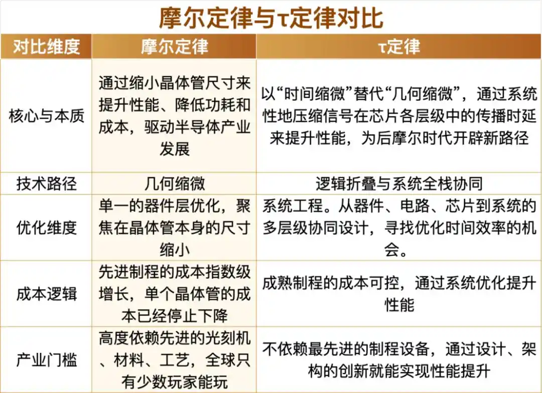
He Tingbo elaborated on this in detail: At the device level, by optimizing transistor and interconnect resistance along with parasitic capacitance, the device-level time constant τ is minimized from the physical foundation to the greatest extent. At the circuit level, logical folding technology breaks through the physical boundaries of traditional planar layouts, significantly shortening the wire length of critical paths and effectively reducing signal propagation resistance and capacitive loads, achieving substantial improvements in transistor density and circuit performance. At the chip level, through full-stack software-architecture-chip co-design, fine-grained control of instruction and data flow based on actual workloads enhances system-level parallelism and efficiency, significantly reducing end-to-end execution time. At the system level, defining the Lingqu Bus reconstructs computing system interconnect protocols, enabling unified memory addressing and native memory semantics across super-nodes, greatly reducing system communication latency.

In comparison, the τ law aligns more closely with the core essence of chip computing power: the primary function of a chip is information processing, and end-users are also more concerned with the latency performance of information processing rather than transistor count or process dimensions. This law provides a completely new technical roadmap for chip design that departs from reliance on pure process scaling, meaning it holds the potential to create chips with satisfactory comprehensive performance even without using the most advanced lithography equipment. Therefore, it is not contradictory to Moore's Law; the two are compatible. It can be understood as: Moore's Law continuously draws finer grids on a flat plane, while the τ Law folds the paper, using three-dimensional space to obtain shorter signal paths.

Notably, the implementation of each layer of the τ law relies on a key player—EDA. It is no longer a "drawing tool" in the traditional sense but has become the central nervous system translating "time miniaturization" from theory into physical chips.

A Huawei paper indicates that on the technical route, a co-existing and superimposed approach of Chiplet advanced packaging, three-dimensional integrated circuits (3DIC), and Logic Folding is adopted to achieve recombination and optimization at different granularities in vertical integration. To achieve hardware integration density improvement exceeding 100-fold by 2035, three major challenges are faced: an EDA toolchain generation gap, cross-wafer process variation, and the law of conservation of energy.

Andrew B. Kahng, Distinguished Professor of Computer Science and Engineering and Electrical and Computer Engineering at the University of California, San Diego, also noted that as the "tailwind" from the traditional "Moore's Law" gradually weakens, these fundamental objectives in EDA and physical design will become increasingly important.

Therefore, EDA has been repositioned to the center of the table.

What New Requirements Does the Tao (τ) Law Pose for EDA?

Regarding the new demands the τ law places on EDA tools and the existing shortcomings of traditional EDA tools, the author engaged in discussions with industry practitioners.

First, the lack of native true 3D design and cross-layer co-optimization capabilities highlights the importance of STCO.

Firstly, Peking University pointed out that traditional 2D design flows, and even the current mainstream "pseudo-3D" flow—where after synthesis each module is "fixed" onto a specific die at once, and then 2D EDA tools are used to implement each die sequentially—cannot achieve cell-level flexible allocation across layers.

Native 3D EDA tools integrate multiple dies into a unified three-dimensional design space, supporting free placement of standard cells across dies while enabling cross-die logic restructuring and global optimization. This provides critical support for translating the logic folding concept from design theory into physical implementation.

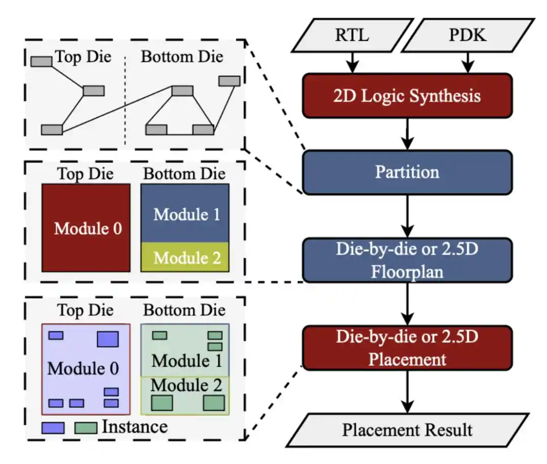
"Pseudo-3D" flow vs. "True-3D" flow. Source: Peking University

Additionally, there is a deficiency in cross-layer co-optimization capabilities. Xpeedic Semiconductor told Semiconductor Industry Insights: Chiplet, 3DIC, and LogicFolding are implementations at different granularities along the same vertical integration main line.

Chiplet combines heterogeneous dies in a 2.5D or 3D manner at the packaging level, moving communication originally within a monolithic SoC to between dies via interconnect standards like UCIe, trading modularity for yield and flexibility. 3DIC further introduces high-density TSVs and hybrid bonding between dies, vertically stacking logic, memory, and analog functions within the same package, compressing interconnect distances from millimeter to micrometer scales. LogicFolding goes a step further—it does not establish interconnects between dies but rather vertically splits and re-distributes "the internal logic of a single chip itself" at the active layer level, allowing the hybrid bonding interface to participate directly in the timing optimization of critical paths like an additional metal layer.

The three are not substitutes but co-exist in a superimposed manner within advanced packaging systems. This superposition brings a fundamental design engineering challenge: when a single package involves UCIe interconnects between Chiplets, inter-layer hybrid bonding in 3D, and intra-die LogicFolding critical path folding, the analysis boundaries for signal integrity, power integrity, thermal distribution, and mechanical stress can no longer be closed independently at any single level.

The proposal of STCO (System-Technology Co-Optimization) aims precisely to break down this fragmentation from a methodological perspective. It demands treating logical architecture, physical layout, multi-physics fields, packaging structure, and even workloads as a unified design space, conducting joint optimization searches across disciplines and abstraction levels. And this capability is the most fundamental gap in the current EDA toolchain.

Second, the lack of multi-physics coupling.

This is one of the most hidden yet critical weaknesses of traditional EDA tools. In the monolithic chip era, power delivery analysis, thermal simulation, and stress calculation belonged to separate, independent toolchains, each with its own modeling, solving, and signoff. But in 3D stacking, this model is no longer fully viable. After vertical integration of multiple dies, power density multiplies, heat dissipation paths become highly asymmetric, and inter-layer temperature differences increase. The resulting thermal expansion mismatch propagates through microbump and hybrid bonding interfaces within the stacked structure, both skewing device electrical characteristics and posing mechanical reliability risks.

What Capabilities Do EDA Vendors Need to Build?

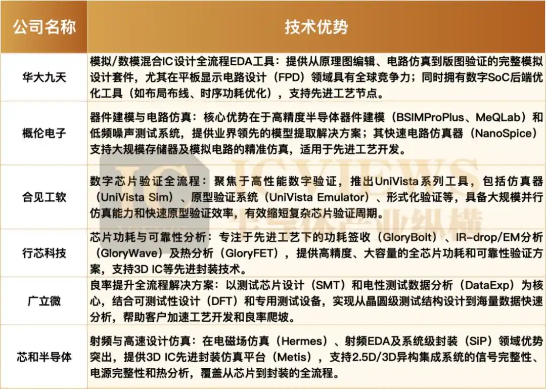
Currently, domestic EDA companies mostly focus on point breakthroughs, tackling tough challenges in their respective specialized segments. From analog simulation to physical verification, from yield enhancement to layout design, a group of excellent domestic EDA enterprises have already formed usable and competitive point tools across many areas.

For example, Empyrean Technology is one of the earliest companies in China engaged in EDA R&D. Empyrean Technology, with analog EDA as its foundation, has gradually expanded into digital, advanced packaging, and other fields, striving to build a full-flow toolchain. Primarius Technologies follows an "underlying penetration" route. It doesn't directly tackle the full flow but relentlessly focuses on device modeling and circuit simulation. UniVista is a leading domestic digital EDA company, representing the full-flow/platform type. Xpeedic Technology chose to show its strength in the most challenging "signoff" stage. Xpeedic Semiconductor primarily focuses on "advanced packaging." Semitronix emphasizes yield enhancement and is the only company capable of forming a complete closed loop through "equipment data collection + software data analysis."

The τ law is expected to propel domestic EDA from "point tool localization" to an industrial software foundation characterized by "full-flow, cross-level, strong co-optimization." This means the EDA toolchain will no longer merely undertake auxiliary functions like circuit drawing, layout design, and backend verification. Instead, it will need to be comprehensively embedded in all key processes across the entire chain: device modeling, PDK construction, circuit simulation, parasitic parameter extraction, timing/power analysis, physical verification, advanced packaging, and system-level co-optimization.

On May 26, the School of Integrated Circuits at Peking University announced a key breakthrough in the prototype of a "true 3D" EDA tool developed to meet the Logic Folding demands of the Tao Law. This tool supports comprehensive three-dimensional space co-optimization, enables cross-die logic free allocation and joint thermal optimization, and can cover designs with tens of millions of instances. Compared to traditional "pseudo-3D" methods, Peking University's "true 3D" EDA achieves: an average wire length reduction of approximately 30%; WNS improvement of about 6%, TNS improvement of about 12%; and a peak temperature reduction of over 3%. The tool has currently completed industrial-level design verification, with subsequent plans to extend to multi-die stacking and heterogeneous integration scenarios, aiming to fill the key gap in 3D chip design.

On the same day, an investor asked Empyrean Technology on an interactive platform: Against the backdrop of the post-Moore era, the industry believes the importance of EDA is evolving from a traditional design tool towards a "system-level performance optimization platform." What is the company's view on the strategic value of future EDA in logic folding, timing optimization, and multi-chip co-optimization?

Empyrean Technology subsequently responded: The company foresightedly observed that current AI, GPU, memory, and other chips are leveraging 3DIC technology to break through the bottlenecks of advanced processes and computing power in the post-Moore era. It has made early-stage layouts in the 3DIC design EDA field, constructing a full-flow solution covering from heterogeneous integrated 3D chip co-design to verification, filling the gap for high-end 3DIC design tools in China, and is the only domestic provider of a full-flow 3DIC design and verification EDA solution. The company launched the first industry-leading Argus 3DIC physical verification platform, fully supporting 2.5D/3D heterogeneous integrated packaging design, enabling full-link physical verification from 3DIC diversified co-design to packaging.

Thus, a path gradually becomes clear: from the theoretical guidance of the τ law, to system architecture definition, and then to the strengthening of the domestic EDA toolchain. In the coming years, vendors who first introduce industrially validated closed-loop solutions for timing closure in logic folding, 3D multi-physics coupling signoff, and full-stack STCO co-optimization are likely to occupy a more proactive position in the "time miniaturization" trend. For domestic EDA, this may provide a window period to shift from point-tool catch-up to building full-stack capabilities—no longer merely aiming for "usable," but continuously evolving towards full-stack "excellent usability."

This article is from the WeChat public account "Semiconductor Industry Insights" (ID: ICViews), author: Feng Ning

İlgili Sorular

QWhat is the core concept of the Tao (τ) Law proposed by Huawei, and how does it differ fundamentally from Moore's Law?

AThe Tao (τ) Law proposes 'time miniaturization' as an alternative to Moore's Law's 'geometric scaling.' Its core is optimizing the time constant (τ) across device, circuit, chip, and system levels to reduce signal delay and improve performance. Unlike Moore's Law's focus on transistor count and chip size, τ Law focuses on optimizing the speed of information processing itself, offering a new technical route that is less dependent on cutting-edge lithography.

QAccording to the article, what new challenges and requirements does the Tao (τ) Law pose for EDA tools?

AThe Tao (τ) Law demands EDA tools to evolve from traditional 2D 'drawing tools' into a central nervous system for 'time miniaturization.' Key new requirements include: 1) Native true-3D design and cross-layer collaborative optimization (STCO) capabilities, moving beyond 'pseudo-3D' flows. 2) The ability to handle multi-physics coupling (e.g., thermal, stress, power integrity) in 3D stacked environments, as these effects can no longer be analyzed in isolation.

QHow do the technical approaches of Chiplet, 3DIC, and LogicFolding relate to each other in the context of implementing the Tao (τ) Law, as described in the article?

AChiplet, 3DIC, and LogicFolding are not mutually exclusive but represent different granularities of vertical integration that coexist and stack within the advanced packaging framework to implement τ Law principles. Chiplet enables modular die integration; 3DIC further reduces interconnect distances via vertical stacking; and LogicFolding takes it a step further by splitting and re-distributing a single chip's internal logic itself across active layers for critical path timing optimization. Their combination necessitates System Technology Co-Optimization (STCO).

QWhat are some examples of Chinese EDA companies mentioned in the article, and what are their respective focuses or strengths?

AThe article mentions several Chinese EDA companies and their specializations: Empyrean (Huada Jiutian): Focuses on full-flow tools, with strength in analog EDA and a claim to be China's only full-flow 3DIC design verification provider. Primarius (Gailun Electronics): Focuses on device modeling and circuit simulation from the bottom up. Unicore (Hejian Gongruan): A leader in digital EDA and full-platform solutions. Xepic (Xingxin Technology): Specializes in sign-off verification. Xpeedic (Xinhe Bandaoti): Focuses on advanced packaging solutions. GigaDevice (Guangliwe): Specializes in yield enhancement through a data-centric closed-loop approach.

QWhat breakthrough related to EDA tools for the Tao (τ) Law was announced by Peking University in May 2026, and what were its reported benefits?

APeking University announced a key breakthrough in a 'true-3D' EDA tool prototype for LogicFolding requirements under the Tao (τ) Law. Compared to traditional 'pseudo-3D' flows, this tool achieved: an average wire length reduction of ~30%, WNS improvement of ~6%, TNS improvement of ~12%, and a peak temperature reduction of over 3%. It supports full 3D spatial co-optimization, cross-die logic allocation, and joint thermal optimization for designs with tens of millions of instances.

İlgili Okumalar

It's Not Jensen Huang Who Wants to Change the PC, But the PC That's Revolting Against Itself

The 40-year-old PC industry is undergoing a fundamental transformation, driven by the rise of AI PCs. At the GTC Taipei 2026 event, NVIDIA, backed by Microsoft and major PC OEMs, announced the RTX Spark super chip for Windows PCs, marking its official entry into the PC core processor market. This move aims to redefine the AI PC by shifting its core from the CPU to an AI-focused SoC (System on Chip). NVIDIA envisions the PC evolving from a personal computer to a "personal AI"—a platform where local AI Agents can autonomously perform tasks. While Intel pioneered the AI PC concept earlier in 2026, NVIDIA's aggressive push, leveraging its vast CUDA developer ecosystem of 6 million, positions it to potentially reshape the industry's long-standing Wintel (Windows-Intel) power structure. NVIDIA's strategy extends beyond hardware; it's about embedding its CUDA, RTX, and AI software stack into the PC platform itself. The article identifies key shifts: 1) The move from a CPU-centric to an AI SoC-centric architecture, similar to Apple's approach with its M-series chips. 2) The PC's evolution from a human-operated tool to a platform for human-Agent collaboration. 3) The extension of NVIDIA's data center-centric CUDA ecosystem to personal devices via RTX Spark. Ultimately, the change is driven by the broader trend of AI moving to personal devices. Companies like Intel, AMD, Qualcomm, and Apple are all participating in this shift. NVIDIA's entry accelerates the competition, but the core driver is the technology itself finding its optimal expression in the PC. The industry is reinventing itself, with the outcome hinging on execution, ecosystem development, and the creation of compelling local AI applications.

marsbit4 saat önce

It's Not Jensen Huang Who Wants to Change the PC, But the PC That's Revolting Against Itself

marsbit4 saat önce

İşlemler

Spot
Futures

Popüler Makaleler

$S$ Nedir

SPERO'yu Anlamak: Kapsamlı Bir Genel Bakış SPERO'ya Giriş İnovasyonun manzarası gelişmeye devam ederken, web3 teknolojilerinin ve kripto para projelerinin ortaya çıkışı dijital geleceği şekillendirmede önemli bir rol oynamaktadır. Bu dinamik alanda dikkat çeken projelerden biri SPERO, $$s$$ olarak adlandırılmaktadır. Bu makale, SPERO hakkında ayrıntılı bilgi toplamak ve sunmak amacıyla, meraklılar ve yatırımcıların web3 ve kripto alanlarındaki temellerini, hedeflerini ve yeniliklerini anlamalarına yardımcı olmayı amaçlamaktadır. SPERO,$$s$$ Nedir? SPERO,$$s$$, kripto alanında merkeziyetsizlik ve blok zinciri teknolojisi ilkelerini kullanarak etkileşimi, faydayı ve finansal kapsayıcılığı teşvik eden bir ekosistem yaratmayı amaçlayan benzersiz bir projedir. Proje, kullanıcıların yenilikçi finansal çözümler ve hizmetler sunarak eşler arası etkileşimleri yeni yollarla kolaylaştırmayı hedeflemektedir. SPERO,$$s$$'nin temel amacı, bireyleri güçlendirmek ve kripto para alanındaki kullanıcı deneyimini artıran araçlar ve platformlar sağlamaktır. Bu, daha esnek işlem yöntemlerini mümkün kılmayı, topluluk odaklı girişimleri teşvik etmeyi ve merkeziyetsiz uygulamalar (dApp'ler) aracılığıyla finansal fırsatlar yaratmayı içermektedir. SPERO,$$s$$'nin temel vizyonu kapsayıcılık etrafında dönmekte olup, geleneksel finansal sistemlerdeki boşlukları kapatmayı ve blok zinciri teknolojisinin faydalarından yararlanmayı hedeflemektedir. SPERO,$$s$$'nin Yaratıcısı Kimdir? SPERO,$$s$$'nin yaratıcısının kimliği bir miktar belirsizdir, çünkü kurucusu(ları) hakkında ayrıntılı arka plan bilgisi sağlayan sınırlı kamuya açık kaynaklar bulunmaktadır. Bu şeffaflık eksikliği, projenin merkeziyetsizlik taahhüdünden kaynaklanabilir—birçok web3 projesinin paylaştığı bir etik anlayışı, bireysel tanınmanın yerine kolektif katkıları önceliklendirmektedir. Topluluk ve onun kolektif hedefleri etrafında tartışmaları merkezileştirerek, SPERO,$$s$$, belirli bireyleri öne çıkarmadan güçlendirme özünü taşımaktadır. Bu nedenle, SPERO'nun etik anlayışını ve misyonunu anlamak, tek bir yaratıcının kimliğini belirlemekten daha önemlidir. SPERO,$$s$$'nin Yatırımcıları Kimlerdir? SPERO,$$s$$, kripto sektöründe yeniliği teşvik etmeye adanmış girişim sermayedarlarından melek yatırımcılara kadar çeşitli yatırımcılar tarafından desteklenmektedir. Bu yatırımcıların odak noktası genellikle SPERO'nun misyonuyla uyumlu olup, toplumsal teknolojik ilerlemeyi, finansal kapsayıcılığı ve merkeziyetsiz yönetimi vaat eden projeleri önceliklendirmektedir. Bu yatırımcı temelleri, yalnızca yenilikçi ürünler sunan projelere değil, aynı zamanda blok zinciri topluluğuna ve ekosistemlerine olumlu katkılarda bulunan projelere de ilgi duymaktadır. Bu yatırımcıların desteği, SPERO,$$s$$'yi hızla gelişen kripto projeleri alanında dikkate değer bir rakip haline getirmektedir. SPERO,$$s$$ Nasıl Çalışır? SPERO,$$s$$, onu geleneksel kripto para projelerinden ayıran çok yönlü bir çerçeve kullanmaktadır. İşte benzersizliğini ve yeniliğini vurgulayan bazı temel özellikler: Merkeziyetsiz Yönetim: SPERO,$$s$$, kullanıcıların projenin geleceğiyle ilgili karar alma süreçlerine aktif olarak katılmalarını sağlayan merkeziyetsiz yönetim modellerini entegre etmektedir. Bu yaklaşım, topluluk üyeleri arasında sahiplik ve hesap verebilirlik duygusunu teşvik etmektedir. Token Kullanımı: SPERO,$$s$$, ekosistem içinde çeşitli işlevler sunmak üzere tasarlanmış kendi kripto para token'ını kullanmaktadır. Bu token'lar, işlemleri, ödülleri ve platformda sunulan hizmetlerin kolaylaştırılmasını sağlayarak genel etkileşimi ve faydayı artırmaktadır. Katmanlı Mimari: SPERO,$$s$$'nin teknik mimarisi, modülerlik ve ölçeklenebilirliği destekleyerek projenin evrimi sırasında ek özelliklerin ve uygulamaların sorunsuz bir şekilde entegrasyonuna olanak tanımaktadır. Bu uyum sağlama yeteneği, sürekli değişen kripto manzarasında geçerliliği sürdürmek için hayati öneme sahiptir. Topluluk Katılımı: Proje, işbirliği ve geri bildirim teşvik eden mekanizmalar kullanarak topluluk odaklı girişimlere vurgu yapmaktadır. Güçlü bir topluluk oluşturarak, SPERO,$$s$$, kullanıcı ihtiyaçlarını daha iyi karşılayabilir ve piyasa trendlerine uyum sağlayabilir. Kapsayıcılığa Odaklanma: Düşük işlem ücretleri ve kullanıcı dostu arayüzler sunarak, SPERO,$$s$$, daha önce kripto alanında yer almamış bireyler de dahil olmak üzere çeşitli bir kullanıcı tabanını çekmeyi hedeflemektedir. Bu kapsayıcılık taahhüdü, erişilebilirlik yoluyla güçlendirme misyonuyla uyumludur. SPERO,$$s$$ Zaman Çizelgesi Bir projenin tarihini anlamak, gelişim yolculuğu ve kilometre taşları hakkında kritik bilgiler sağlar. Aşağıda, SPERO,$$s$$'nin evriminde önemli olayları haritalayan önerilen bir zaman çizelgesi bulunmaktadır: Kavram Geliştirme ve Fikir Aşaması: SPERO,$$s$$'nin temelini oluşturan ilk fikirler, blok zinciri endüstrisindeki merkeziyetsizlik ve topluluk odaklılık ilkeleriyle yakından uyumlu olarak geliştirildi. Proje Beyaz Kağıdının Yayınlanması: Kavramsal aşamayı takiben, SPERO,$$s$$'nin vizyonunu, hedeflerini ve teknolojik altyapısını ayrıntılı bir şekilde açıklayan kapsamlı bir beyaz kağıt yayımlandı ve topluluk ilgisini ve geri bildirimini toplamak amacıyla sunuldu. Topluluk Oluşturma ve Erken Katılımlar: Projenin hedefleri etrafında tartışmalar yürüterek destek toplamak ve erken benimseyenler ile potansiyel yatırımcılar için bir topluluk oluşturmak amacıyla aktif iletişim çabaları gerçekleştirildi. Token Üretim Etkinliği: SPERO,$$s$$, yerel token'larını erken destekçilere dağıtmak ve ekosistem içinde başlangıç likiditesini sağlamak amacıyla bir token üretim etkinliği (TGE) gerçekleştirdi. İlk dApp'in Yayınlanması: SPERO,$$s$$ ile ilişkili ilk merkeziyetsiz uygulama (dApp) faaliyete geçti ve kullanıcıların platformun temel işlevleriyle etkileşimde bulunmalarını sağladı. Sürekli Gelişim ve Ortaklıklar: Projenin tekliflerine sürekli güncellemeler ve iyileştirmeler yapılmakta olup, blok zinciri alanındaki diğer oyuncularla stratejik ortaklıklar, SPERO,$$s$$'yi rekabetçi ve gelişen bir oyuncu haline getirmiştir. Sonuç SPERO,$$s$$, web3 ve kripto paranın finansal sistemleri devrim niteliğinde dönüştürme ve bireyleri güçlendirme potansiyelinin bir kanıtıdır. Merkeziyetsiz yönetime, topluluk katılımına ve yenilikçi tasarlanmış işlevselliğe olan bağlılığıyla, daha kapsayıcı bir finansal manzaraya doğru bir yol açmaktadır. Hızla gelişen kripto alanındaki herhangi bir yatırımda olduğu gibi, potansiyel yatırımcılar ve kullanıcılar, SPERO,$$s$$ içindeki devam eden gelişmelerle ilgili olarak kapsamlı bir araştırma yapmaları ve düşünceli bir şekilde katılmaları teşvik edilmektedir. Proje, kripto endüstrisinin yenilikçi ruhunu sergileyerek, sayısız olasılığını keşfetmeye davet etmektedir. SPERO,$$s$$'nin yolculuğu hala devam ederken, temel ilkeleri, teknoloji, finans ve birbirimizle etkileşim biçimimizi etkileyebilir.

89 Toplam GörüntülenmeYayınlanma 2024.12.17Güncellenme 2024.12.17

$S$ Nedir

AGENT S Nedir

Agent S: Web3'te Otonom Etkileşimin Geleceği Giriş Web3 ve kripto para dünyasında sürekli gelişen manzarada, yenilikler bireylerin dijital platformlarla etkileşim biçimlerini sürekli olarak yeniden tanımlıyor. Bu tür öncü projelerden biri olan Agent S, açık ajans çerçevesi aracılığıyla insan-bilgisayar etkileşimini devrim niteliğinde değiştirmeyi vaat ediyor. Otonom etkileşimlerin yolunu açarak, Agent S karmaşık görevleri basitleştirmeyi ve yapay zeka (AI) alanında dönüştürücü uygulamalar sunmayı hedefliyor. Bu detaylı inceleme, projenin karmaşıklıklarına, benzersiz özelliklerine ve kripto para alanındaki etkilerine dalacaktır. Agent S Nedir? Agent S, bilgisayar görevlerinin otomasyonunda üç temel zorluğu ele almak üzere özel olarak tasarlanmış çığır açıcı bir açık ajans çerçevesidir: Alan Spesifik Bilgi Edinimi: Çerçeve, çeşitli dış bilgi kaynaklarından ve iç deneyimlerden akıllıca öğrenir. Bu çift yönlü yaklaşım, alan spesifik bilgi açısından zengin bir veri havuzu oluşturmasını sağlar ve görev yürütmedeki performansını artırır. Uzun Görev Ufukları Üzerinde Planlama: Agent S, karmaşık görevlerin verimli bir şekilde parçalanmasını ve yürütülmesini kolaylaştıran deneyim artırımlı hiyerarşik planlama kullanır. Bu özellik, çoklu alt görevleri etkili ve verimli bir şekilde yönetme yeteneğini önemli ölçüde artırır. Dinamik, Homojen Olmayan Arayüzlerle Başlama: Proje, ajanlar ve kullanıcılar arasındaki etkileşimi geliştiren yenilikçi bir çözüm olan Ajan-Bilgisayar Arayüzü'ni (ACI) tanıtmaktadır. Çok Modlu Büyük Dil Modellerini (MLLM'ler) kullanarak, Agent S çeşitli grafik kullanıcı arayüzlerini sorunsuz bir şekilde gezinebilir ve manipüle edebilir. Bu öncü özellikler aracılığıyla, Agent S, makinelerle insan etkileşimini otomatikleştirmede karşılaşılan karmaşıklıkları ele alan sağlam bir çerçeve sunarak, AI ve ötesinde birçok uygulama için zemin hazırlıyor. Agent S'nin Yaratıcısı Kimdir? Agent S'nin kavramı temelde yenilikçi olsa da, yaratıcısı hakkında spesifik bilgiler belirsizliğini koruyor. Yaratıcı şu anda bilinmiyor, bu da projenin yeni aşamasını veya kurucu üyeleri gizli tutma stratejik tercihini vurguluyor. Anonimlikten bağımsız olarak, odak çerçevenin yetenekleri ve potansiyeli üzerinde kalıyor. Agent S'nin Yatırımcıları Kimlerdir? Agent S, kriptografik ekosistemde oldukça yeni olduğundan, yatırımcıları ve finansal destekçileri hakkında ayrıntılı bilgiler açıkça belgelenmemiştir. Projeyi destekleyen yatırım temelleri veya organizasyonları hakkında kamuya açık bilgilerdeki eksiklik, finansman yapısı ve gelişim yol haritası hakkında sorular doğuruyor. Destekleyicilerin anlaşılması, projenin sürdürülebilirliğini ve potansiyel pazar etkisini değerlendirmek için kritik öneme sahiptir. Agent S Nasıl Çalışır? Agent S'nin temelinde, çeşitli ortamlarda etkili bir şekilde çalışmasını sağlayan son teknoloji bir sistem yatmaktadır. İşleyiş modeli birkaç ana özellik etrafında inşa edilmiştir: İnsan Benzeri Bilgisayar Etkileşimi: Çerçeve, bilgisayarlarla etkileşimleri daha sezgisel hale getirmeyi amaçlayan gelişmiş AI planlaması sunar. Görev yürütmedeki insan davranışını taklit ederek, kullanıcı deneyimlerini yükseltmeyi vaat eder. Anlatı Belleği: Yüksek düzeyde deneyimlerden yararlanmak için kullanılan Agent S, görev geçmişlerini takip etmek amacıyla anlatı belleğini kullanarak karar verme süreçlerini geliştirir. Episodik Bellek: Bu özellik, kullanıcılara adım adım rehberlik sağlayarak, çerçevenin görevler gelişirken bağlamsal destek sunmasına olanak tanır. OpenACI Desteği: Yerel olarak çalışabilme yeteneği ile Agent S, kullanıcıların etkileşimleri ve iş akışları üzerinde kontrol sağlamasına olanak tanır ve Web3'ün merkeziyetsiz felsefesiyle uyumlu hale gelir. Dış API'lerle Kolay Entegrasyon: Çeşitli AI platformlarıyla uyumluluğu ve çok yönlülüğü, Agent S'nin mevcut teknolojik ekosistemlere sorunsuz bir şekilde entegre olmasını sağlar ve geliştiriciler ile organizasyonlar için cazip bir seçenek haline getirir. Bu işlevsellikler, Agent S'nin kripto alanındaki benzersiz konumuna katkıda bulunarak, karmaşık, çok aşamalı görevleri minimum insan müdahalesi ile otomatikleştirir. Proje geliştikçe, Web3'teki potansiyel uygulamaları dijital etkileşimlerin nasıl gelişeceğini yeniden tanımlayabilir. Agent S'nin Zaman Çizelgesi Agent S'nin gelişimi ve kilometre taşları, önemli olaylarını vurgulayan bir zaman çizelgesinde özetlenebilir: 27 Eylül 2024: Agent S'nin kavramı, “Bilgisayarları İnsan Gibi Kullanan Açık Bir Ajans Çerçevesi” başlıklı kapsamlı bir araştırma makalesi ile tanıtıldı ve projenin temelini sergiledi. 10 Ekim 2024: Araştırma makalesi arXiv'de kamuya açık olarak yayınlandı ve çerçevenin derinlemesine bir incelemesini ve OSWorld benchmark'ına dayalı performans değerlendirmesini sundu. 12 Ekim 2024: Agent S'nin yetenekleri ve özellikleri hakkında görsel bir içgörü sağlayan bir video sunumu yayımlandı ve potansiyel kullanıcılar ve yatırımcılarla daha fazla etkileşim sağlandı. Bu zaman çizelgesindeki işaretler, sadece Agent S'nin ilerlemesini değil, aynı zamanda şeffaflık ve topluluk katılımına olan bağlılığını da göstermektedir. Agent S Hakkında Ana Noktalar Agent S çerçevesi gelişmeye devam ederken, birkaç ana özellik öne çıkmakta ve yenilikçi doğasını ve potansiyelini vurgulamaktadır: Yenilikçi Çerçeve: İnsan etkileşimine benzer bir bilgisayar kullanımı sağlamak üzere tasarlanan Agent S, görev otomasyonuna yeni bir yaklaşım getiriyor. Otonom Etkileşim: GUI aracılığıyla bilgisayarlarla otonom olarak etkileşim kurabilme yeteneği, daha akıllı ve verimli hesaplama çözümlerine doğru bir sıçrama anlamına geliyor. Karmaşık Görev Otomasyonu: Sağlam metodolojisi ile karmaşık, çok aşamalı görevleri otomatikleştirerek süreçleri daha hızlı ve daha az hata payı ile gerçekleştirebilir. Sürekli İyileştirme: Öğrenme mekanizmaları, Agent S'nin geçmiş deneyimlerden öğrenmesini sağlar ve sürekli olarak performansını ve etkinliğini artırır. Çok Yönlülük: OSWorld ve WindowsAgentArena gibi farklı işletim ortamlarında uyumlu olması, geniş bir uygulama yelpazesine hizmet edebilmesini sağlar. Agent S, Web3 ve kripto alanında kendini konumlandırırken, etkileşim yeteneklerini artırma ve süreçleri otomatikleştirme potansiyeli, AI teknolojilerinde önemli bir ilerlemeyi temsil etmektedir. Yenilikçi çerçevesi aracılığıyla, Agent S dijital etkileşimlerin geleceğini örneklemekte ve çeşitli sektörlerde kullanıcılar için daha sorunsuz ve verimli bir deneyim vaat etmektedir. Sonuç Agent S, AI ve Web3'ün birleşiminde cesur bir sıçramayı temsil ediyor ve teknoloji ile etkileşim biçimimizi yeniden tanımlama kapasitesine sahip. Henüz erken aşamalarında olmasına rağmen, uygulama olanakları geniş ve çekici. Kritik zorlukları ele alan kapsamlı çerçevesi ile Agent S, otonom etkileşimleri dijital deneyimin ön plana çıkmasına taşımayı hedefliyor. Kripto para ve merkeziyetsizlik alanlarına daha derinlemesine girdikçe, Agent S gibi projelerin teknoloji ve insan-bilgisayar işbirliğinin geleceğini şekillendirmede önemli bir rol oynayacağı kesin.

578 Toplam GörüntülenmeYayınlanma 2025.01.14Güncellenme 2025.01.14

AGENT S Nedir

S Nasıl Satın Alınır

HTX.com’a hoş geldiniz! Sonic (S) satın alma işlemlerini basit ve kullanışlı bir hâle getirdik. Adım adım açıkladığımız rehberimizi takip ederek kripto yolculuğunuza başlayın. 1. Adım: HTX Hesabınızı OluşturunHTX'te ücretsiz bir hesap açmak için e-posta adresinizi veya telefon numaranızı kullanın. Sorunsuzca kaydolun ve tüm özelliklerin kilidini açın. Hesabımı Aç2. Adım: Kripto Satın Al Bölümüne Gidin ve Ödeme Yönteminizi SeçinKredi/Banka Kartı: Visa veya Mastercard'ınızı kullanarak anında Sonic (S) satın alın.Bakiye: Sorunsuz bir şekilde işlem yapmak için HTX hesap bakiyenizdeki fonları kullanın.Üçüncü Taraflar: Kullanımı kolaylaştırmak için Google Pay ve Apple Pay gibi popüler ödeme yöntemlerini ekledik.P2P: HTX'teki diğer kullanıcılarla doğrudan işlem yapın.Borsa Dışı (OTC): Yatırımcılar için kişiye özel hizmetler ve rekabetçi döviz kurları sunuyoruz.3. Adım: Sonic (S) Varlıklarınızı SaklayınSonic (S) satın aldıktan sonra HTX hesabınızda saklayın. Alternatif olarak, blok zinciri transferi yoluyla başka bir yere gönderebilir veya diğer kripto para birimlerini takas etmek için kullanabilirsiniz.4. Adım: Sonic (S) Varlıklarınızla İşlem YapınHTX'in spot piyasasında Sonic (S) ile kolayca işlemler yapın.Hesabınıza erişin, işlem çiftinizi seçin, işlemlerinizi gerçekleştirin ve gerçek zamanlı olarak izleyin. Hem yeni başlayanlar hem de deneyimli yatırımcılar için kullanıcı dostu bir deneyim sunuyoruz.

1.6k Toplam GörüntülenmeYayınlanma 2025.01.15Güncellenme 2026.06.02

S Nasıl Satın Alınır

Tartışmalar

HTX Topluluğuna hoş geldiniz. Burada, en son platform gelişmeleri hakkında bilgi sahibi olabilir ve profesyonel piyasa görüşlerine erişebilirsiniz. Kullanıcıların S (S) fiyatı hakkındaki görüşleri aşağıda sunulmaktadır.

活动图片