$25 Billion: Tesla Buys the Lowest-Tier Entry Ticket to the Chip Arms Race

marsbit2026-03-16 tarihinde yayınlandı2026-03-16 tarihinde güncellendi

Özet

Elon Musk has announced Tesla's plan to invest approximately $25 billion to build a semiconductor superfab named "Terafab," targeting 2nm process technology with a production capacity of 100,000 wafers per month. The move aims to address Tesla's soaring demand for AI chips, driven by its autonomous driving systems, Optimus robots, and upcoming Robotaxi fleet, which existing foundries like TSMC and Samsung cannot fully support. However, the $25 billion budget is considered insufficient by industry standards. For comparison, TSMC’s Arizona fab costs $165 billion, Samsung’s Taylor fab $44 billion, and Intel’s Ohio project $28 billion. A standard 2nm fab with 50,000 wafers/month typically requires around $28 billion, meaning Tesla’s goal is highly ambitious. Tesla’s chip development has been rapid: from HW3 (14nm, 144 TOPS) to AI5 (3/2nm, 2000+ TOPS), with performance multiplying every generation. Its growing reliance on external foundries led to a $16.5 billion long-term deal with Samsung for AI6 production. Terafab represents a natural shift toward self-sufficiency. The project faces significant challenges, including a 3–5 year construction period and additional time for production ramp-up. If Tesla follows industry timelines, Terafab may not be operational until 2029–2030, coinciding with expected mass production of Optimus and Robotaxi. Musk has also hinted at potential collaboration with Intel, which has advanced 18A process capacity. The $25 billion investment buys Tesl...

Musk is going to make his own chips. Not design—Tesla has been designing its own chips for seven years. This time, it's manufacturing. He announced an investment of approximately $25 billion to build a chip superfab named Terafab, targeting a 2nm process, with a monthly output of 100,000 wafers, integrating logic chips, memory, and advanced packaging within the same facility.

The reason behind this isn't complicated. Tesla's appetite for computing power has grown so large that external foundries can't keep up. Each generation of its autonomous driving chips sees a three to fivefold increase in computing power, with the Optimus robot and Robotaxi nearing mass production. Meanwhile, the world's most advanced process wafer capacity has already been snapped up by Apple, Qualcomm, and NVIDIA. Securing capacity through foundry contracts is just a stopgap measure; building their own fab is the endgame.

$25 billion. In other industries, this sum could buy an entire supply chain. In semiconductor manufacturing, it's not even enough to build a standard 2nm wafer fab.
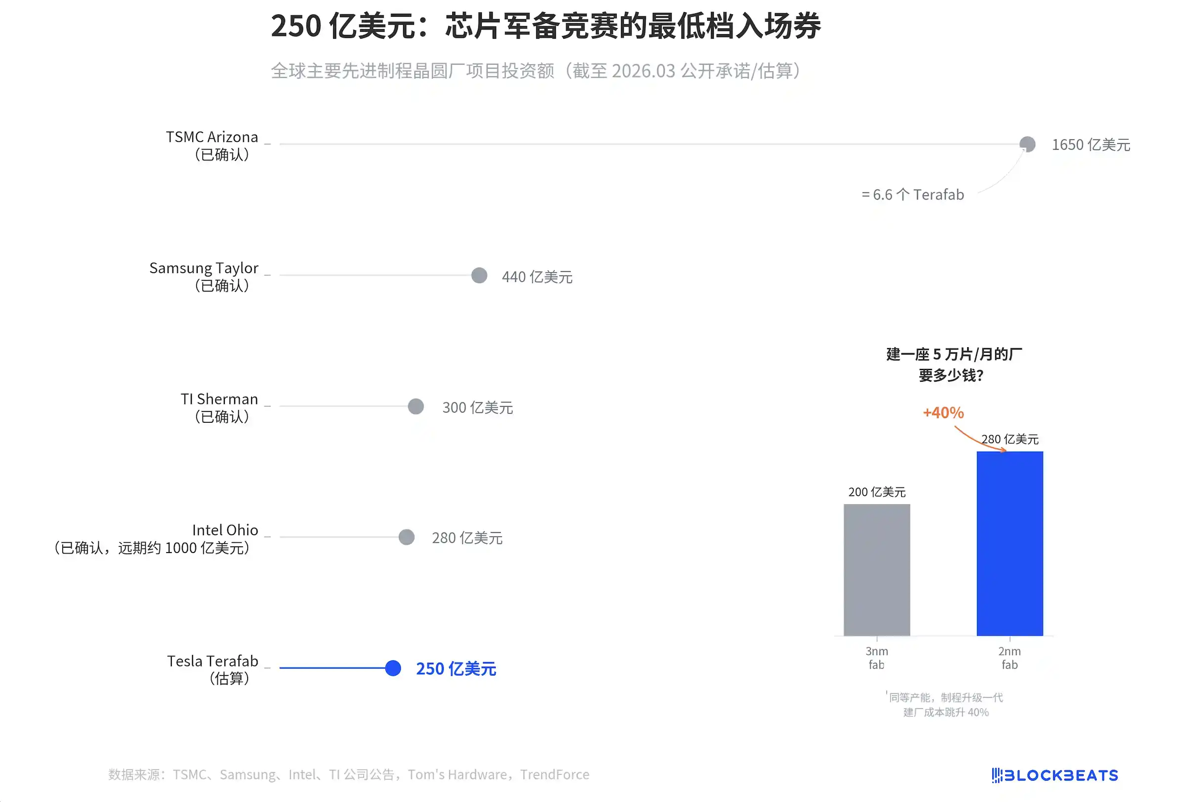
According to company announcements and industry media reports, the total investment for TSMC's Arizona campus is $165 billion, Samsung's Taylor fab is $44 billion, analog chip leader Texas Instruments' (TI) Sherman fab is $30 billion, and Intel's Ohio fab is $28 billion. Tesla ranks last. Furthermore, according to estimates by Tom's Hardware and other media outlets, its $25 billion is only an external推算 (calculation/speculation), and Musk himself has not confirmed an exact figure.

More crucially, look at the small chart on the right. According to estimates by industry research firms, building a fab with a monthly capacity of 50,000 wafers costs $20 billion for 3nm and $28 billion for 2nm. Moving from 3nm to 2nm, the construction cost jumps by 40%.

Tesla wants to achieve a monthly output of 100,000 2nm wafers with $25 billion. Based on industry benchmarks, a single 50,000 wafers/month 2nm fab alone costs $28 billion. Tesla aims to do the work of two fabs plus a packaging facility with less money than one standard fab. This isn't a budget; it's a wish list.

But what truly makes one gasp about Terafab isn't the money; it's the capacity target.

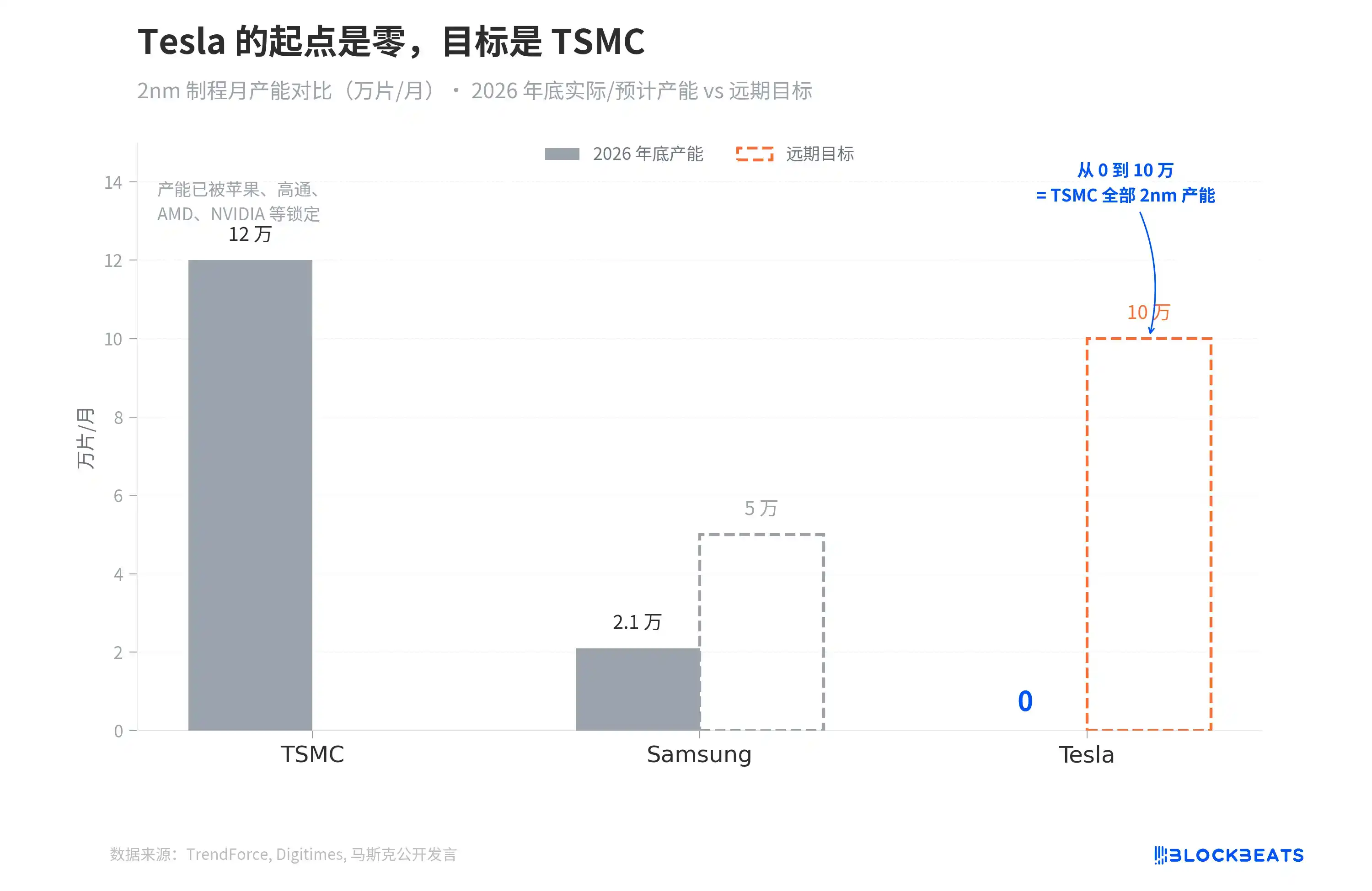
According to data from industry research firm TrendForce, TSMC's 2nm capacity is expected to be 100,000 to 130,000 wafers/month by the end of 2026, but this number has already been pre-booked by Apple, Qualcomm, AMD, and NVIDIA. According to a Digitimes report, Samsung's 2nm capacity is only 21,000 wafers/month, with a long-term target of 50,000.

Tesla's starting point is zero. The target is 100,000.

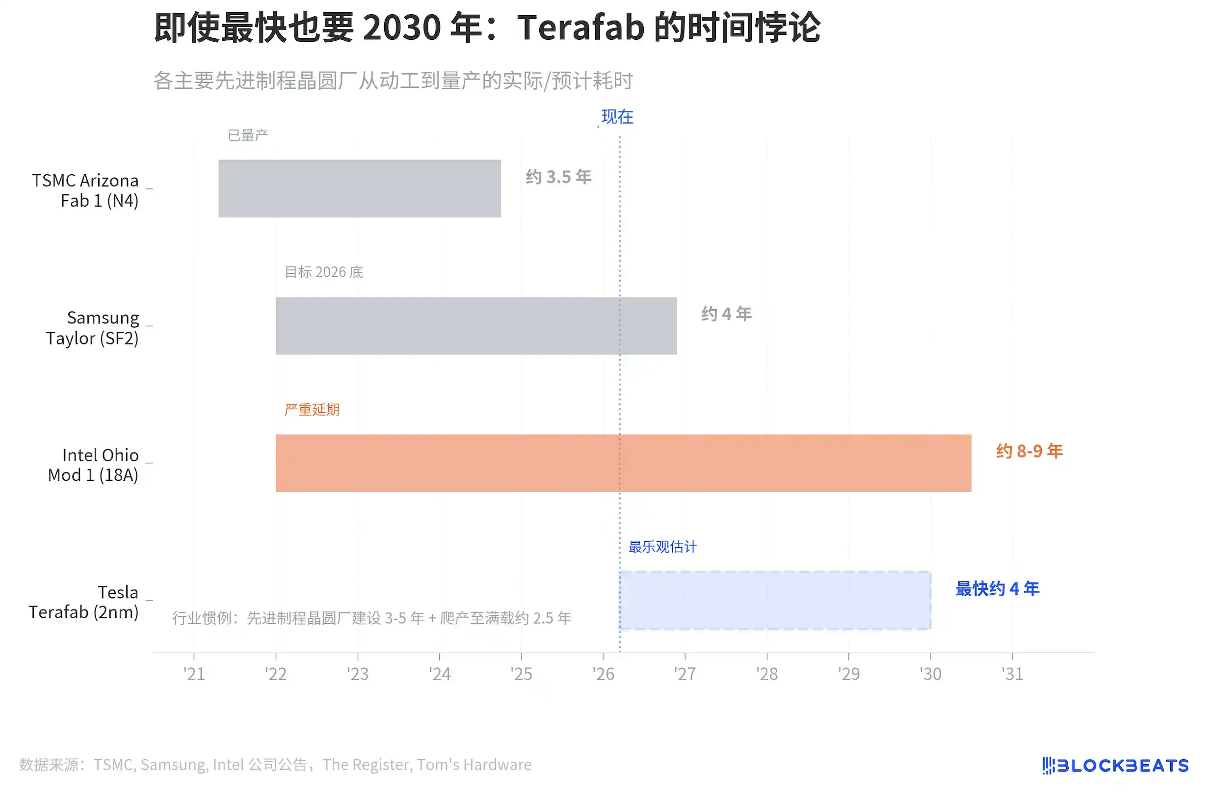
Going from 0 to 100,000 wafers/month equals starting from scratch to catch up with TSMC's entire global capacity for the most advanced process. TSMC started building its fab in Arizona in 2021 and took three and a half years to get its first 4nm fab into mass production. And TSMC has thirty years of manufacturing experience accumulated in Taiwan.

Tesla's manufacturing speed for cars did exceed everyone's expectations. But the margin for error in wafer manufacturing and vehicle manufacturing is not on the same scale. A flaw in a car can be recalled; a defect on a wafer means thousands of chips are scrapped.
To understand why Terafab is appearing in 2026, one must look at a longer timeline.

In 2019, the team led by Tesla's autonomous driving chip chief architect, Jim Keller, delivered HW3. This was Tesla's first fully self-developed autonomous driving chip, manufactured by Samsung on 14nm, with 144 TOPS. In 2023, HW4 upgraded to Samsung's 7nm, more than tripling the computing power. According to a TrendForce report, by AI5 in 2026, the process jumps to dual sourcing with 3nm and 2nm, with computing power直奔 (heading straight for) 2000 to 2500 TOPS, and it strips out the GPU and ISP entirely, optimizing the entire chip solely for transformer inference.

Each generation sees a three to fivefold performance increase. But the foundry strategy has also been evolving simultaneously. From HW3's "Samsung only," to AI5's "dual sourcing from TSMC and Samsung as a hedge," to AI6. According to TechCrunch and Bloomberg reports, for AI6, they directly signed a $16.5 billion long-term contract with Samsung to lock in capacity until 2033.
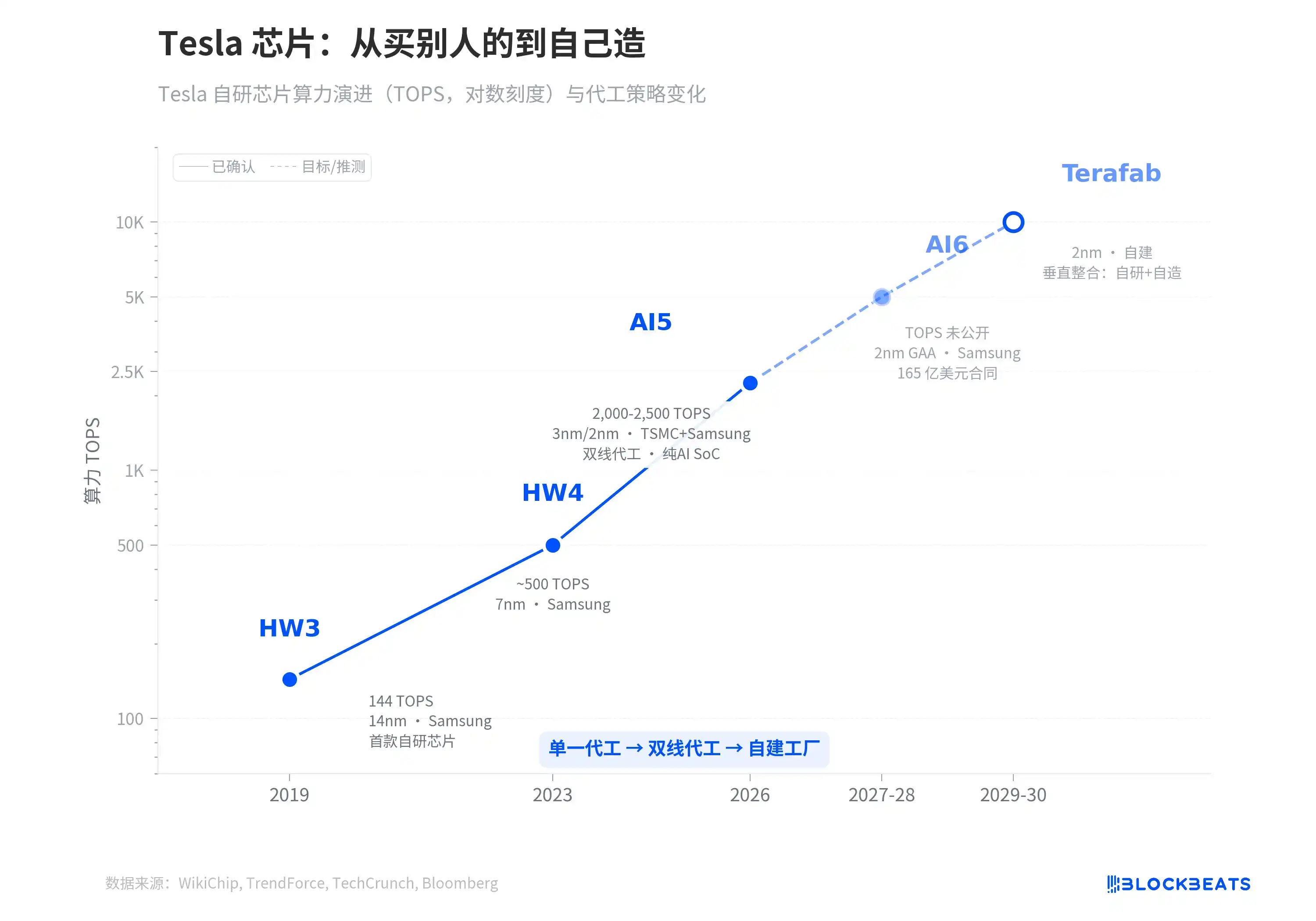
Terafab is the natural extension of this timeline. According to a Tom's Hardware report, last year Tesla's AI6 contract essentially saved Samsung's Taylor fab, that $44 billion factory which had been搁置 (shelved) due to "having no customers." When your chip demand is large enough to sustain someone else's wafer fab, the next question is, why not build your own.

The AI6 and Terafab nodes on the chart's dashed line segment are not labeled with specific TOPS because the specifications for these two generations have not been publicly released. But the trend direction is clear. The computing power curve of Tesla's chips is exponential, and the reliance on foundries has reached a point where it must be resolved.

The remaining question is time.

TSMC Arizona Fab 1 took about 3.5 years from groundbreaking to mass production, the industry's fastest record, but TSMC has thirty years of manufacturing积累 (accumulation). Samsung Taylor took about 4 years, pausing in the middle due to lack of customers. According to The Register, Intel Ohio is the worst, starting in 2022 and now delayed until 2030 or 2031.

Industry惯例 (convention) is 3 to 5 years for construction, plus another 2.5 years to ramp up to full capacity. Even giving Tesla TSMC's speed, Terafab would at the earliest start outputting wafers by the end of 2029.

And this恰好 (coincides) with Tesla's computing power bottleneck window. The dual sourcing for AI5 can last until 2027-2028, and the Samsung contract for AI6 covers until 2033. But if the mass production scale of the Optimus robot and Robotaxi explodes as Musk plans by 2029, external foundry capacity will likely be insufficient. Terafab doesn't need to produce chips in 2026; it needs to be ready by 2030.
Musk has also publicly discussed the possibility of cooperation with Intel. Intel has its most advanced 18A process (equivalent to the industry's 2nm level) and idle capacity desperately needing external customers; Tesla has clear chip demand and money. If this path materializes, Terafab wouldn't be starting from scratch alone, but a marriage of convenience where each gets what they need.

$25 billion doesn't buy much certainty in chip manufacturing. But it bought an entry ticket. A ticket that transforms Tesla from the biggest buyer of chips into a player in chip manufacturing. Looking back at this chart three years from now, it will either be the starting point of Tesla's vertical integration strategy, or Musk's most expensive pie-in-the-sky promise.

İlgili Sorular

QWhat is the name of Tesla's new chip manufacturing plant and what is its target production capacity and process node?

ATesla's new chip manufacturing plant is named Terafab, with a target production capacity of 100,000 wafers per month at the 2nm process node.

QWhy is Tesla building its own chip fab instead of relying solely on external foundries like TSMC and Samsung?

ATesla's demand for computing power, driven by its autonomous driving chips, Optimus robots, and Robotaxi plans, has grown so large that external foundries cannot keep up. The most advanced production capacity is already allocated to companies like Apple, Qualcomm, and NVIDIA, making building its own fab a long-term necessity.

QHow does the cost of Tesla's Terafab ($25 billion) compare to the investments of other major semiconductor manufacturers in their new fabs?

ATesla's estimated $25 billion investment is at the lower end compared to other major projects: TSMC's Arizona campus costs $165 billion, Samsung's Taylor fab is $44 billion, Texas Instruments' Sherman fab is $30 billion, and Intel's Ohio fab is $28 billion.

QWhat is the industry's estimated timeline for building a new fab and reaching full production, and how does this relate to Tesla's needs?

AThe industry standard is 3-5 years for construction and an additional 2.5 years to ramp up to full production. Even at TSMC's record speed of 3.5 years, Terafab would not produce chips until late 2029, which aligns with the expected surge in demand from Optimus and Robotaxi around 2030.

QWhat potential partnership did Musk mention to accelerate Terafab's goals, and what would each party gain?

AElon Musk mentioned a potential partnership with Intel. Intel would provide its advanced 18A process (equivalent to 2nm) and underutilized capacity, while Tesla would bring clear chip demand and capital, making it a mutually beneficial arrangement.

İlgili Okumalar

In Conversation with Ray Dalio: We Are Currently in an AI Bubble, with 1% of My Portfolio in Bitcoin

Ray Dalio, founder of Bridgewater Associates, warns in an interview that the current AI boom shows classic bubble characteristics, which could lead to significant economic downturns as seen in past cycles like 1929 or 2000. He explains that speculative enthusiasm, fueled by debt and overvaluation, often precedes a crash when rising rates or taxation force asset sales, causing widespread losses and recession. Dalio also outlines his "Big Cycle" theory, describing an approximate 80-year pattern where widening wealth gaps, massive government deficits, and shifting geopolitical power (like China's rise) create internal conflict and global instability. He emphasizes that we are in a late-cycle, transitional phase where traditional powers like the US and UK face decline. For personal wealth protection, Dalio advises diversification beyond cash into assets like stocks, bonds, real estate, and particularly gold, which he prefers over Bitcoin. While he holds about 1% of his portfolio in Bitcoin as a non-printable hard asset, he views gold as more secure from technological or governmental threats. Regarding AI's impact, Dalio believes it will disproportionately benefit capital owners, worsening inequality by replacing both physical and cognitive labor. He suggests that human intuition and emotional intelligence, combined with AI, will be key for future workers. On taxation, Dalio argues that wealth taxes are impractical and risk triggering asset sell-offs, reducing productive investment. He points to the UK as a cautionary example of debt, low productivity, and political strife. Geopolitically, Dalio foresees a more regionalized world, with the US showing weakness in prolonged conflicts like with Iran, akin to past imperial declines. The ideal outcome, he suggests, is coexisting powerful blocs (e.g., Americas, China-Asia Pacific) without major war.

marsbit39 dk önce

In Conversation with Ray Dalio: We Are Currently in an AI Bubble, with 1% of My Portfolio in Bitcoin

marsbit39 dk önce

Daily 7.2 Trillion KRW: Foreign Capital's Record Net Buying on Friday! Wall Street Says Headwinds for Korean Stock Fund Flows Have Subsided

South Korean stock market sees a dramatic shift in fund flows. On July 31, foreign investors made a record net purchase of approximately KRW 7.2 trillion in KOSPI stocks, marking a fundamental reversal from the persistent large-scale net outflows seen in previous months. This contributed to a significant narrowing of foreign net selling in July to KRW 9.8 trillion, down sharply from KRW 48.4 trillion in June and KRW 44.5 trillion in May. Simultaneously, domestic institutional pressure eased. South Korean pension funds and asset managers turned to a net buying position in July, purchasing KRW 1.0 trillion worth of KOSPI shares, contrasting with net sales in May and June. Market volatility is expected to be dampened by new financial regulations. Effective July 31, the Financial Services Commission tightened access for retail investors to single-stock leveraged ETFs by raising the minimum cash deposit requirement. Trading volumes for these products subsequently dropped to about 50% of their monthly average. Citigroup Research maintains its year-end KOSPI target of 10,000 points. The firm cites several supportive factors: the substantial easing of headwinds from capital outflows, a robust fundamental outlook for the semiconductor sector, historically low market valuations, strong economic fundamentals, and the potential for policy support from financial authorities if needed.

marsbit39 dk önce

Daily 7.2 Trillion KRW: Foreign Capital's Record Net Buying on Friday! Wall Street Says Headwinds for Korean Stock Fund Flows Have Subsided

marsbit39 dk önce

Thanks to Dice Rolls, Bitcoin Keys Are Stored Offline, But Not Everyone Will Do It

The article discusses using dice rolls to generate secure Bitcoin wallet seeds, providing entropy independent of potentially flawed hardware random number generators. It explains that each fair dice roll offers about 2.585 bits of entropy, with around 50 rolls needed for a standard 12-word seed phrase and 99+ recommended for higher security. This method gained attention after a vulnerability was revealed in some Coldcard hardware wallets, where a faulty firmware RNG (dating back to 2021) compromised generated keys. The analysis notes that while a dice-generated main seed was safe from this specific flaw, other Coldcard functions (like creating paper wallets, backup keys, or passwords) could still be vulnerable if they used the defective RNG. The piece argues that while dice-based entropy is technically robust, the manual process is error-prone, tedious, and unrealistic for most new users, who might make mistakes in recording or inputting rolls. It concludes that while manual entropy generation should remain an option for advanced users, the long-term goal is to develop reliable, user-friendly hardware and software that securely generates randomness without requiring specialized knowledge. Coldcard users are advised to check their firmware version and replace any secondary secrets (like paper wallet keys) created with vulnerable devices, while also considering multi-signature setups with devices from different manufacturers for added security.

cryptonews.ru5 saat önce

Thanks to Dice Rolls, Bitcoin Keys Are Stored Offline, But Not Everyone Will Do It

cryptonews.ru5 saat önce

İşlemler

Spot
活动图片