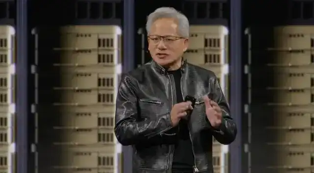
On May 25, 2026, He Tingbo, Huawei Director and President of the Semiconductor Business Unit, officially introduced the Tao (τ) Law at ISCAS 2026. This marks China's first proposal of a new principle guiding the global semiconductor industry development.
1. τ (tau, transliterated as "Tao") represents the time constant in circuit theory—the time required for a signal to switch from one state to another. A smaller τ indicates faster circuit switching.
The traditional Moore's Law pursues continuously shrinking transistor dimensions (geometric scaling).
The Tao Law shifts towards temporal scaling: continuously compressing signal propagation delay, without relying on extreme linewidths.
2. Core Implementation Path—Logic Folding
Traditional chip circuit layouts are two-dimensional planes, requiring signals to travel long distances laterally. Logic folding expands the circuit layout from a single layer to a multi-layer stack, "folding" critical paths vertically, replacing long-distance planar interconnects with short-distance vertical interconnects, thereby significantly reducing the time constant τ.
3. Achievements and Goals
Over the past six years, Huawei has designed and mass-produced 381 chips adhering to the Tao Law.
Plans to launch a Kirin chip using logic folding technology in the autumn of 2026.
It is projected that by 2031, high-end chips based on the Tao Law can achieve performance levels equivalent to a 1.4nm process node.
This article compiles a list of companies related to Huawei's Tao Law below. It is recommended to like and save this list for future research. The content is solely for logical interpretation and information reference, not investment advice. Follow me for daily analysis of core market themes and logic.
(I) Design Software EDA
The Tao Law requires optimization at the circuit level for transistor and interconnect layout to compress the time constant τ, and EDA tools permeate the entire chip design, simulation, and verification process. The 381 chips Huawei has mass-produced must rely on a mature, full-flow domestic EDA tool system. The following companies hold core positions in the EDA field:
1. Huada Jiutian
Ranked first in A-share EDA tool market share, holds about 6% domestic market share, currently the largest and most comprehensive EDA enterprise in China in terms of scale and product line. The company possesses full-flow EDA tool systems for analog circuit design, digital circuit design EDA tools, etc., capable of providing underlying support for the circuit-level optimization required by the Tao Law.
2. Primarius Technologies
Ranked second in A-share EDA tool market share, core advantages lie in device modeling and verification EDA tools. The company has formed a complete toolchain covering device modeling, circuit simulation, and yield analysis. The Tao Law's requirement for fine optimization of transistor interconnect resistance and capacitance can directly interface with Huawei's chip design flow through Primarius's device physics modeling capabilities.
3. Semitronix
Ranked third in A-share EDA tool market share, specializes in EDA manufacturing tools, particularly chip yield enhancement and test chip design. The yield enhancement solutions provided by the company are a key bridge between wafer foundries and design houses. As logic folding technology moves towards mass production, the yield ramp-up process will highly depend on yield management EDA tools like those from Semitronix.
4. Shentong Metro
Indirectly holds a stake (approx. 7.58%) in Huada Jiutian through its subsidiary fund, Jianyuan Fund. Shentong Metro itself is not a pure-play EDA company, but as a significant shareholder of Huada Jiutian, it stands to benefit indirectly from the valuation uplift cycle of domestic EDA driven by the Tao Law.
5. Anlogic
Has independently developed a full-flow FPGA-dedicated EDA software—TangDynasty. FPGA EDA tools are extremely difficult; Anlogic is one of the few domestic companies capable of providing end-to-end tools from logic synthesis to place & route. The Tao Law emphasizes architectural innovation; FPGAs are indispensable in verification and prototyping simulation. Anlogic's EDA tools will indirectly benefit from the demand for domestic FPGAs and supporting tools within the Huawei ecosystem.
6. Sai Microelectronics
Holds an investment stake (4.67%) in Qingdao Zhan Cheng Technology, which focuses on IC design EDA tools, specializing in physical verification and layout-related areas. Sai Microelectronics itself is a MEMS foundry; its investment in EDA forms a two-way synergy between manufacturing and tools.
7. Fudan Microelectronics
Possesses full-flow, independently developed FPGA supporting EDA tools capable of supporting its self-developed FPGA products. The company holds a prominent position in the domestic high-reliability FPGA field; its EDA tools have undergone extensive internal validation. Logic folding designs promoted by the Tao Law might be first applied in FPGA chips; Fudan Microelectronics's hardware-software integration capability will benefit.
8. Zhangjiang Hi-Tech
As the development entity of Zhangjiang Science City, participates in investing in the Shanghai EDA Innovation Center, dedicated to building a full-flow domestic EDA ecosystem. The company follows more of an industrial platform and ecosystem investment logic, not directly involved in EDA development, but benefits from regional industrial cluster dividends.
9. Taiji Industry
Independently develops and procures EDA software for high-power semiconductor product design. The company's main business is power semiconductors. Although different from the advanced logic chip EDA market, the "architecture over process" concept advocated by the Tao Law might also permeate the power device sector. Taiji Industry's self-developed EDA capability becomes its differentiating highlight.
10. Aerospace Hi-Tech
Has established its own integrated circuit EDA design platform, mainly used for the autonomous design of its aerospace-grade chips. The company has deep expertise in high-reliability, radiation-hardened chips. Its self-built EDA platform reflects the demand for design tool autonomy and control, aligning with the independent innovation logic behind the Tao Law.
11. Dongtu Technology
Holds a stake in Zhongke Yihai Micro; the latter's team independently developed EDA tools supporting its FPGA products. Dongtu Technology indirectly possesses FPGA EDA capability through its investment, offering some thematic elasticity in the wave of domestic substitution.
12. Yue Dianli A
Its participating subsidiary, Shenzhen Capital Group (SCGC), previously invested in Huada Jiutian. Yue Dianli A holds a multi-layered, indirect stake in Huada Jiutian. It belongs to a very indirect beneficiary target with a long equity chain, offering relatively limited elasticity.
(II) Chiplet & Advanced Packaging
Logic folding upgrades circuit layout from a single-layer planar structure to a multi-layer stack, essentially using 3D packaging to achieve vertical short-distance interconnects. This creates a rigid demand for advanced packaging technologies: multi-layer chip stacking, Through-Silicon Vias (TSV), hybrid bonding, and other processes become essential. The following companies are core participants in domestic advanced packaging and Chiplet technology:
1. Tongfu Microelectronics
Ranked first in domestic advanced packaging technology progress, has mass-produced Chiplet-architecture CPU/GPU products for AMD at scale. The company possesses a complete 2.5D/3D packaging platform, including processes like TSV, Fan-out, Hybrid Bonding. AMD is the most successful benchmark in Chiplet commercialization. As AMD's core packaging and testing partner, Tongfu Microelectronics has fully operationalized the entire flow from technology to mass production, making it the most likely candidate to undertake packaging needs for Huawei's logic folding chips.
2. JCET Group
Ranked second in domestic advanced packaging technology progress, has mass-produced various advanced packaging products (e.g., SiP, Fan-out, WLCSP, etc.). JCET is the world's third-largest packaging and testing foundry, with significant scale advantages. Although its current scale orders in the Chiplet field are not as large as Tongfu Microelectronics', its vast capacity and customer base give it rapid follow-up capability.
3. Tianshui Huatian Technology
Ranked third in domestic advanced packaging technology progress, has achieved mass production of advanced packaging products. The company focuses on high-density packaging, with deployments in areas like FC, TSV, SiP. Huatian's advantages lie in cost control and customer responsiveness; it is expected to capture a portion of packaging orders once logic folding technology matures.
4. Yong Silicon Electronics
Advanced packaging business accounts for nearly 100% of revenue, a pure-play advanced packaging company. The company focuses on high-end packaging and testing, with products including QFN, BGA, SiP, etc. Due to its smaller size and high business purity, the company often exhibits greater earnings elasticity within the Tao Law theme.
5. Cambricon Technologies
Its cloud AI chip, Siyuan 370, already employs Chiplet technology, a typical commercial chip case of Chiplet architecture domestically. Cambricon is an AI chip design company, not directly involved in packaging, but its successful Chiplet experience proves the feasibility of this technical path. The Tao Law will further promote the adoption of Chiplet in AI chips; as a pioneer, Cambricon may gain first-mover advantage in design methodology.
6. VeriSilicon
Provides high-end application processor platforms based on Chiplet architecture. VeriSilicon is a chip design service (IP and design platform) company with a rich Chiplet IP library and system integration capabilities. The multi-layer stacking design promoted by the Tao Law will increase demand for Chiplet design methods, interface IP, and Network-on-Chip (NoC). VeriSilicon's platform capabilities are expected to translate into growth in licensing revenue.
7. Blue Rocket Electronics
Products cover packaging forms like DNF, PDFN, QFN, etc., with QFN being a basic type in advanced packaging and testing. The company's technical level is within the domestic mainstream tier, benefiting from the overall semiconductor packaging and testing recovery and domestic substitution logic.
8. Zizheng Shares
Mainly engaged in specialized equipment for semiconductor back-end advanced packaging, such as die bonders, sorters, etc. In the advanced packaging capacity expansion cycle, equipment suppliers are among the first to benefit.
9. Dagang Shares
The company's subsidiary, Suzhou Koyang Optoelectronics, possesses advanced packaging technology expertise, mainly engaged in wafer-level packaging, TSV, etc. Currently, it is still in the stage of technology accumulation and market expansion.
10. Suzhou Good-Ark
Involves in the advanced packaging field through investments and subsidiaries, currently in the technology accumulation stage. The company's main business is semiconductor discrete devices.
11. Sanjia Technology
The company involves in semiconductor packaging molds and equipment; in the advanced packaging field, it is in the technology accumulation stage.
(III) Foundry Manufacturing
Compressing the time constant τ relies not only on circuit design but also requires optimization at the device level for transistor structure, interconnect materials, and process parameters. These optimizations must ultimately be implemented in the process platforms and design rules of wafer fabrication plants. Furthermore, the logic folding Kirin chip Huawei plans to launch in autumn 2026 must be taped out and mass-produced by a foundry. Major domestic foundries all have the opportunity to undertake this historic order:
1. SMIC
The absolute leader in wafer foundry in Mainland China, ranked fourth globally and first nationally. The company possesses mature 14nm and improved processes, along with FinFET advanced node capabilities. The logic folding technology advocated by the Tao Law is essentially design-process co-optimization. As the most technologically advanced domestic foundry, SMIC is most likely to become the primary supplier for Huawei's new-generation Kirin chips. The company also benefits from the capacity transfer trend across the entire domestic chip industry chain.
2. Hua Hong Semiconductor
Ranked sixth globally and second nationally in wafer foundry, known for power devices, analog chips, and embedded non-volatile memory. Although Hua Hong's advanced node capability is weaker than SMIC's, it has deep expertise in specialty processes. The "logic folding" of the Tao Law does not necessarily depend on extreme linewidths like 5nm/3nm. Hua Hong's mature nodes combined with innovative 3D stacking designs might also undertake some of Huawei's edge computing or IoT chip foundry needs.
3. Nexchip Semiconductor
Ranked ninth globally and third nationally in wafer foundry, primarily engaged in DDIC (Display Driver IC), MCU, etc. The company's technology nodes are mainly 40nm-90nm mature processes. Although there is a gap with cutting-edge logic chip foundry, within the entire industry chain localization process driven by the Tao Law, Nexchip is expected to gain more mature node order transfers from domestic design companies.
4. Yan Dong Microelectronics
Specializes in discrete devices, analog ICs, and specialty IC foundry, with annual revenue of about 2.056 billion RMB. The company's products mainly target high-reliability and industrial control fields. The radiation effect of the Tao Law might influence the design methodology of analog mixed-signal chips. Yan Dong Microelectronics, as a specialty IC foundry, benefits from the overall domestic substitution trend.
Last Sunday, many 20% limit-up stocks appeared among the premium research reports shared within the planet community, such as Rong Da Gan Guang, ACM Research Shanghai last Thursday/Friday. Last night's Hua Xing Yuan Chuang, Hua Hong Semiconductor, SMIC, Xin Lei Neng, etc. For daily premium research reports, please view them in the planet circle on the homepage of this account.
Solemn Statement: All content in this account is solely for information and logic organization, for study and discussion purposes, and does not constitute any investment advice. The publication of articles has no association whatsoever with the stock movements of any related companies. Do not use this as a basis for investment decisions. You must make independent investment decisions. The market involves risks; investment requires caution.