With the continuous surge in demand for training and inference of large AI models, the performance bottleneck of computing chips has shifted from the computing unit to memory bandwidth. HBM (High Bandwidth Memory) has become the core constraint for the iteration of high-end AI hardware. At the HotChips 2026 International High-Performance Chip Technology Conference, the world's two leading memory giants, Samsung and SK Hynix, collectively disclosed the future technology roadmap for HBM4, breaking the industry's long-standing iteration logic for HBM.
Compared to the previous simple approach of increasing DRAM speed and stacking layers, the new-generation HBM4 architecture comprehensively shifts towards three innovative directions: Base Die logic process upgrades, hybrid bonding 3D stacking, and EMIB heterogeneous hybrid packaging. Behind this technological iteration is HBM's transformation from a single memory device into an integrated system of "memory + logic + packaging + IP + EDA."
The HBM Evolution Logic Shifts from Die Speed-up to System Optimization
In the previous iteration cycles of HBM3 and HBM3E, the industry's technology upgrade logic was relatively fixed. Core optimizations focused primarily on the DRAM memory die itself, achieving steady improvement in overall bandwidth by increasing single-die transfer rates, adding stacking layers, and optimizing micro-bump interconnect structures. Under this framework, the bottom Base Die only served passive bridging roles, handling simple signal relaying, power distribution, and testing assistance. Its process architecture long followed mature memory-derived processes, requiring no large-scale iterations. The entire HBM product's technological barriers and production bottlenecks were entirely concentrated in the DRAM manufacturing stage.
However, with the exponential growth in AI computing power demand, the marginal effects of the traditional iteration model are rapidly diminishing. In ultra-high bandwidth scenarios, simply increasing DRAM speed leads to severe issues like signal crosstalk, power consumption spikes, and timing skew. Optimizations in the two-dimensional plane are no longer sufficient for ultra-large computing workloads. Addressing this industry pain point, at this year's HotChips 2026 conference, Samsung and SK Hynix simultaneously released new technological concepts, clarifying that the core breakthrough point in the HBM4 era is no longer the memory die, but the systemic reconstruction of the underlying Base Die.
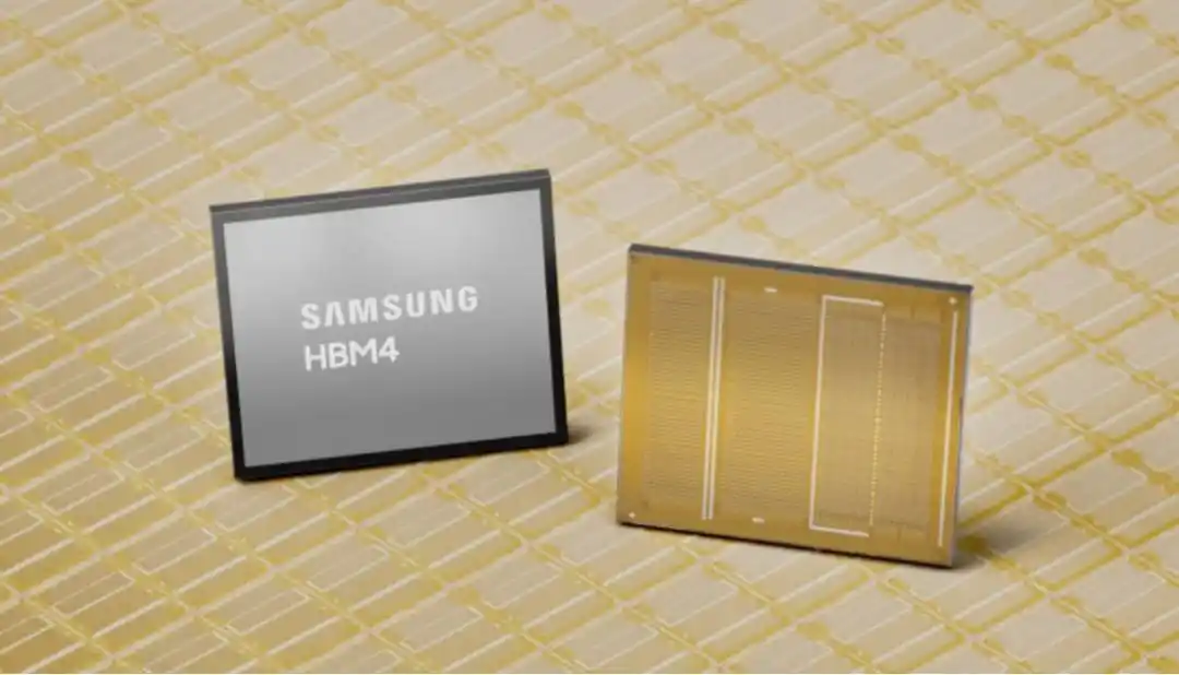
The two manufacturers have formed distinctly differentiated technological paths. In its HotChips presentation, Samsung disclosed that its HBM4/HBM4E products' Base Die will use its own 4nm logic process, with C-Die using the 1cDRAM node, achieving a maximum pin speed of up to 11.7 Gbps, scalable to 13 Gbps, with single-stack bandwidth reaching up to 3.3 TB/s. Leveraging the high-density transistor advantages of the logic process, the Base Die can integrate higher-performance PHY circuits, signal error-correction modules, and power management units, significantly optimizing high-speed signal integrity and solving timing disorder issues under ultra-high bandwidth. Simultaneously, Samsung clearly stated in its architectural design that it will sink part of the memory control logic to the Base Die, effectively freeing up GPU die area for expanding compute units.
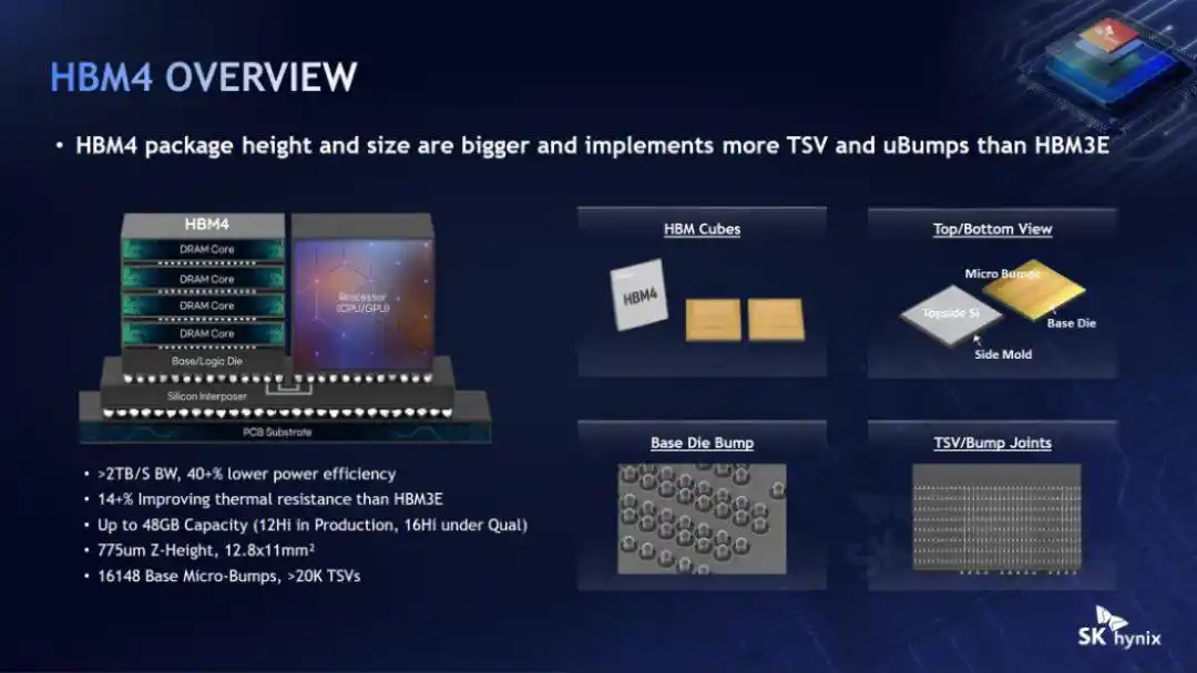
SK Hynix has adopted a division-of-labor collaboration iteration model, choosing to partner with TSMC. Its Base Die uses TSMC's 12nm logic process. Compared to Samsung's fully in-house logic architecture, SK Hynix's solution focuses more on mass production stability, optimizing the Base Die's power delivery network and thermal conduction structure to meet the heat dissipation and load requirements of ultra-high stacking architectures like 12-layer or even 16-layer. The differentiated approaches of these two routes mean the internal logic architecture of HBM4 Base dies is no longer uniform. Products from different manufacturers naturally differ in process, performance, and application scenarios, adding entirely new complexities for subsequent supply chain adaptation and chip design iterations.
Switching the Base Die to a logic process brings multiple benefits. Logic processes enable higher transistor density, optimizing the signal integrity and power control of PHY circuits, allowing them to handle HBM4's doubled 2048-bit I/O width. Additionally, the surplus chip area on the Base Die provides hardware space for near-memory computing. HBM no longer serves merely as a data container; it can perform simple data preprocessing inside the memory, alleviating the data movement pressure of the von Neumann architecture. However, the cost is also significant: HBM is no longer a product memory manufacturers can complete entirely in-house. Logic foundry capacity, IP design capabilities, and cross-process collaborative simulation all become constraints for HBM mass production. DRAM manufacturers need deep collaboration with logic foundries, design, verification, and tape-out cycles are lengthened, and supply chain complexity multiplies.
Multiple Advanced Packaging Paths Proceed in Parallel
Another key signal from HotChips 2026: HBM's system integration packaging paths are diversifying. TSMC's CoWoS is no longer the sole solution; hybrid packaging solutions are taking the stage, while internal stacking bonding technology transitions towards hybrid bonding 3D stacking.
SK Hynix confirmed in its presentation that it is evaluating Intel's EMIB (Embedded Multi-die Interconnect Bridge) technology for 2.5D system integration between HBM4 and computing chips. Traditional CoWoS relies on a single large-area silicon interposer to handle all signal interconnections between the GPU and HBM. It offers excellent performance but comes with high interposer costs. Furthermore, constrained by lithography machine reticle size limits, capacity expansion is difficult. Global CoWoS capacity has long been in short supply, with leading customers prioritizing capacity allocation, leaving other manufacturers facing long wait times for production line access. EMIB abandons the full silicon interposer, embedding tiny silicon bridges only in local areas where chip signals interact. Organic substrates handle most of the routing, while local silicon bridges handle high-density, high-speed signal transmission. This solution can reduce packaging costs, break through reticle size limitations, and enable larger-scale multi-chip integration. Google's TPU has already included EMIB in its next-generation solution shortlist.
However, EMIB does not mean a direct replacement for CoWoS. In extremely high-density signal scenarios, EMIB's local silicon bridges still have gaps compared to full silicon interposers in terms of signal loss and power integrity. SK Hynix's positioning is to treat EMIB as an important supplementary route, not a wholesale replacement. High-end training chips will likely still prioritize CoWoS, while mid-to-high-end inference chips and large-scale computing accelerators can use EMIB solutions to alleviate packaging capacity pressure, forming a dual-path parallel situation.
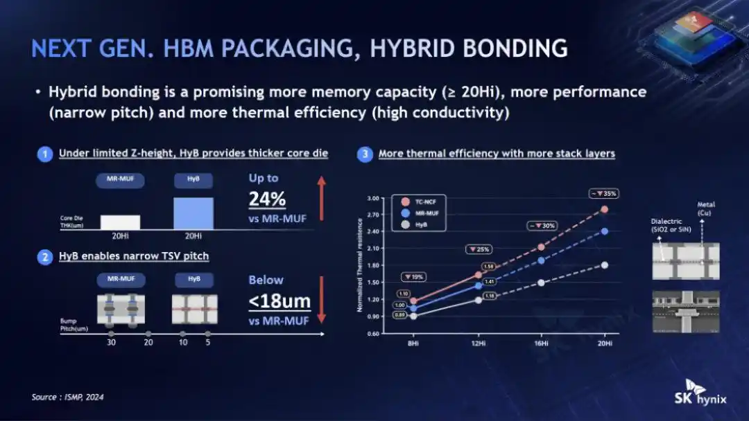
Regarding the bonding technology inside the HBM stack, i.e., between the multiple DRAM dies, it is currently in a transition period from MR-MUF (Mass Reflow Molded Underfill) to Hybrid Bonding. For the current mass-production version of HBM4, the mainstream still uses MR-MUF, TCNCF thermal compression bonding solutions, relying on micro-bumps for inter-layer connections. However, as stacking layers push towards 16, the pitch, thermal resistance, and power consumption of micro-bumps are gradually reaching physical limits. Compared to MR-MUF, Hybrid Bonding can not only increase core chip thickness by 24%, reduce TSV pitch below 18 microns, but also, when increasing stacking layers, significantly lower thermal resistance by 35%. This technology is expected to debut earliest in HBM5, targeting ultra-high stacking of 16 to 20 layers and beyond.
Nevertheless, Hybrid Bonding is currently still in the small-batch validation stage. Challenges remain in yield control, equipment costs, and thin-wafer handling. It will not see large-scale commercial adoption in 2026. The industry generally expects Hybrid Bonding to see scaled adoption in the HBM4E iterative version or HBM5 generation around 2027-2028.
This creates a very special technological transitional phase for the current HBM industry: For the new-generation HBM4 product, the external system integration is pioneering diversified exploration with EMIB heterogeneous packaging to alleviate high-end packaging capacity pressure. Meanwhile, the internal DRAM stacking still adheres to mature MR-MUF thermal compression processes to ensure mass production stability, with Hybrid Bonding reserved for pre-research and future layout. The simultaneous advancement of multiple technology paths and the coexistence of old and new processes significantly amplifies the uncertainty in current HBM4 technology selection.
Furthermore, thermal management has officially become an unavoidable core bottleneck for ultra-high-stack HBM. The 16-layer stacking architecture substantially increases the overall thermal load of HBM. Heat accumulation directly leads to bandwidth throttling and failure to run at full performance. Addressing this pain point, both manufacturers have proposed differentiated solutions: SK Hynix introduced the iHBM (Internal Heat-conducting Component) solution, embedding highly thermally conductive yet electrically insulating cooling components into the D2D PHY area of the HBM to create dedicated heat dissipation paths, reducing thermal resistance by an additional 30% or more and improving system operational stability. Samsung has planned a copper thermal path design for its future HBM5 products, aiming to solve the heat dissipation challenge of ultra-high stacking from the hardware structural level. It is clear that the performance ceiling of future high-stack HBM products will no longer be determined solely by bandwidth and speed parameters but will be directly dictated by thermal management capabilities.
IP and 3D EDA Become the Invisible Core Barriers for HBM4
Today, the core barriers for HBM4 are not limited to manufacturing and packaging; they have extended into two soft-power domains: high-speed IP and heterogeneous EDA toolchains, becoming the most easily overlooked yet most critical bottlenecks in the current industry. As HBM4 interface speeds break through 9 Gbps and I/O widths double in capacity, the design difficulty of high-speed PHY and SerDes interface IP increases exponentially.
High-speed IP is not simple circuit design; it requires deep adaptation to DRAM die characteristics, Base Die logic architecture, and packaging wiring structure, along with joint simulation and debugging for signal integrity and power integrity. Currently, global mature, mass-production-grade HBM4 high-speed IP resources are highly concentrated. A few overseas leading vendors, leveraging years of tape-out experience, monopolize the IP support market for mainstream computing chips. For small and medium-sized chip design firms and emerging supply chain players, the inability to access mature high-speed IP means they cannot adapt to the HBM4 architecture, creating a stringent industry entry barrier.
Simultaneously, shortcomings in 3D heterogeneous EDA toolchains further amplify the challenges in HBM4 implementation. HBM4 is a typical multi-process, multi-die heterogeneous integrated system. The logic base, memory stack, and silicon bridge/interposer packaging belong to different process systems. Traditional two-dimensional discrete EDA tools cannot perform cross-die, cross-process collaborative simulation. In 3D stacking scenarios, electrical, thermal, and mechanical effects are coupled; simulation deviations in a single link can lead to overall design convergence failure.
There is a clear fragmentation issue in the current mainstream industry design flow. Front-end logic design, mid-end physical implementation, and back-end packaging simulation data cannot be shared or reused, leading to extremely high iteration costs. HotChips 2026 clearly pointed out that the scaled adoption of HBM4 highly depends on integrated 3DIC co-design toolchains that enable full-process linkage across design, process, packaging, and multi-physics simulation. The adaptability of EDA tools and the debugging compatibility of high-speed IP directly determine the mass production yield and performance ceiling of HBM4, constituting core technical barriers currently difficult for small and medium-sized manufacturers to overcome.
Overall, this conference completely outlines the new evolutionary path for the HBM industry: It is moving away from the traditional single-point hardware iteration model and stepping into a system-level competition era characterized by collaborative upgrades in architecture, packaging, process, and hardware-software ecosystems. The differentiated technological paths of Samsung and SK Hynix have broken the industry's long-standing standardized landscape. The long-term coexistence of old and new processes, scenario-based technological stratification, and system capabilities determining success will become the core development norms for the HBM track in the next 2-3 years, rewriting the competition rules of the AI memory industry.
This article is from the WeChat public account "Semiconductor Industry Review" (ID: ICViews), author: Zihao.