At the Hot Chips conference, both Samsung and SK Hynix agreed that GPUs, memory, foundry, and packaging must be designed as a system. From that point on, their solutions began to diverge.
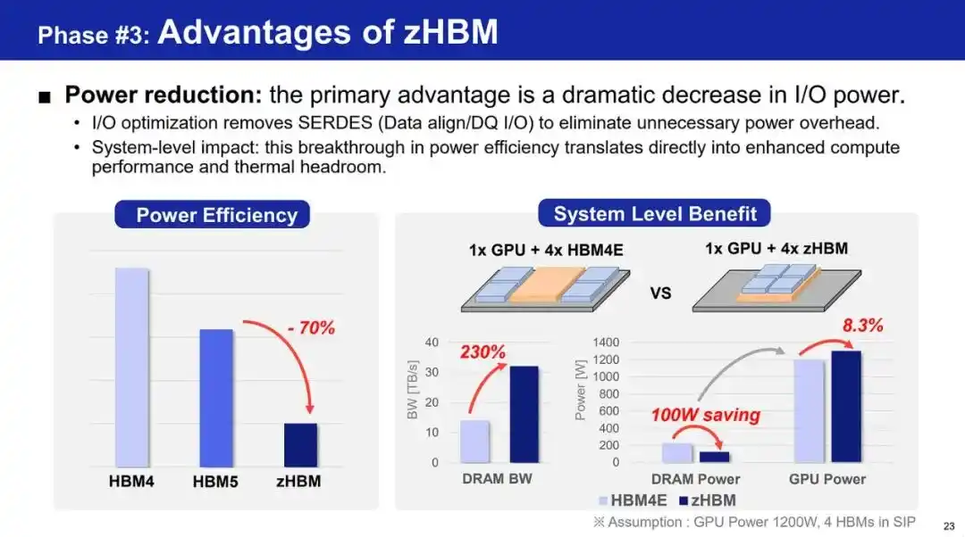
Samsung is transforming the base die into an active part of the system. It plans to move the memory controller from the GPU up to the logic base die, freeing 5–10% of GPU area for more compute and potentially improving performance by 10–20%. Selective AI operations can also run on the base die to reduce data movement. In the long term, it is pushing zHBM technology, which directly stacks the GPU and DRAM, expected to reduce DRAM power consumption by about 70% while more than doubling bandwidth.
SK Hynix is focusing on higher stacking and managing the resulting heat and warpage issues. It confirmed that 12-layer HBM4 stacking has entered production, while the 16-layer version has entered customer validation. Hybrid bonding is the path to 20-layer and higher stacking, allowing for thicker dies and tighter pitches. Its iHBM approach adds a dedicated thermal conduction path inside the hottest areas of the stack. The competition is no longer just about bandwidth and capacity. Base die architecture and advanced packaging are becoming decisive battlegrounds.
Samsung's Custom Base Die Based on Logic Nodes
In a 2026 Hot Chips presentation, Samsung Electronics unveiled zHBM, the ultimate evolution of High Bandwidth Memory. This concept discards the 2.5D interposer, vertically stacking DRAM on top of computing chips like GPUs to form a true 3D integration architecture, aiming to reduce DRAM power consumption by 70% and increase bandwidth by 2.3x compared to HBM4E.
Samsung outlined a three-phase roadmap, transforming the base die from a passive data transfer channel to an active computing partner. Phase 1 moves the memory controller from the xPU to the base die to reclaim silicon area; Phase 2 adds memory expansion and attention compute capabilities to the base die; Phase 3 ultimately achieves zHBM.
Next, let's take a look at Samsung's proposal.
At the presentation, they provided some charts showing the development trends for HBM5 specifications. While nothing is final yet, it's interesting to look at the chart in the top right corner.
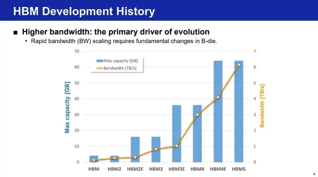
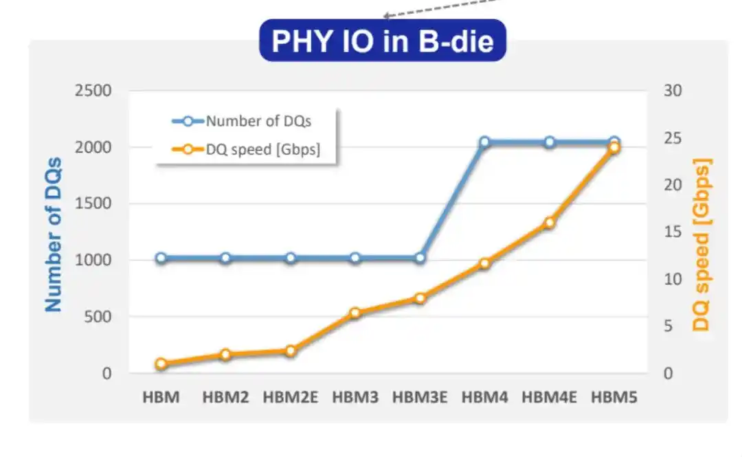
A 60GB, 6 TB/s HBM5 package sounds great. Let's do the math. 6 TB/s bandwidth with 2048 channels implies a per-pin data rate of 23.5 Gbps. Our current state-of-the-art is 16 Gbps, which is a huge leap, and using an advanced logic node could achieve this. With a capacity of 3 GB per die and a total of 60 GB, that means a stack height of 20 layers.
In another slide, Samsung confirmed a per-pin data rate of 16 Gbps for HBM4E. Our earlier calculation for HBM5 is also validated in the chart below.
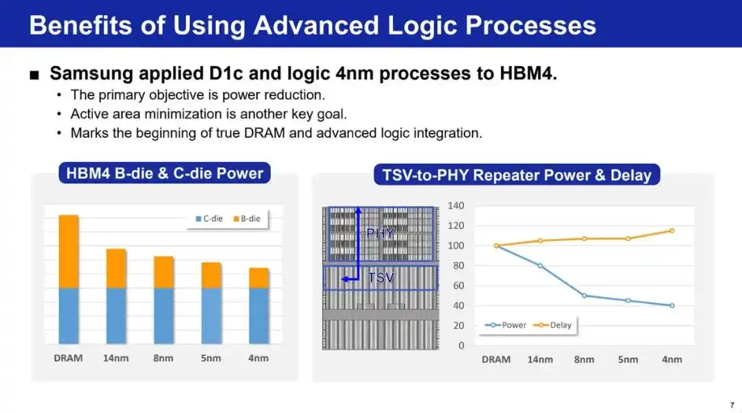
Samsung's apparent advantage lies in its internally developed logic die, whereas Micron and SK Hynix need to collaborate with others to obtain it. Samsung emphasizes this advantage here and explains the importance of a custom die. Samsung uses 1C process for memory and 4nm process for logic, significantly reducing the die's power consumption. The diagram below subtly criticizes Micron, which uses a DRAM process to fabricate the logic die in its HBM4 memory dies.
Even better, as mentioned earlier, Samsung clearly divides its product roadmap into three phases. We will introduce them one by one.
Phase 1: Low-Hanging Fruit
When the base die is built on a logic node, the physical area of the HBM PHY module shrinks, and power efficiency improves. This means the inter-die module connecting the HBM and xPU will be smaller. This has two advantages:
Increase area within the xPU for more compute;
Increase usable area on the HBM base die for more advanced features.
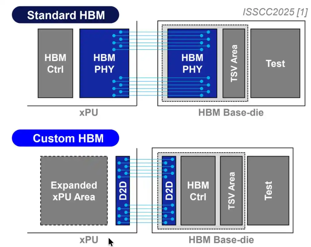
The downside of the size reduction is higher thermal density in these regions. Interestingly, they provided the actual sizes of PHY modules across different HBM generations.
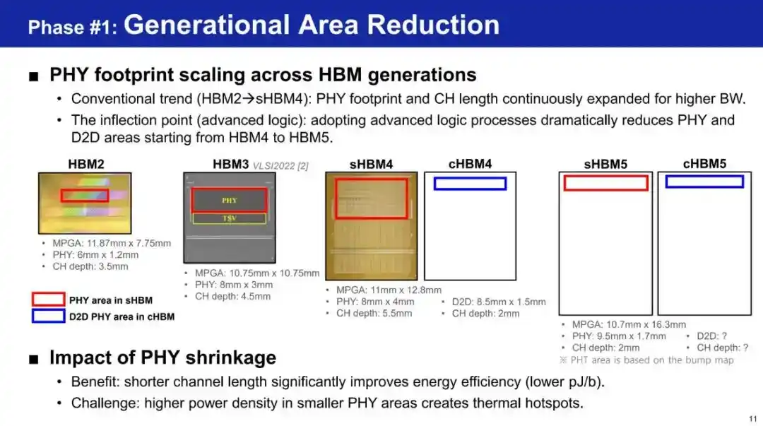
Samsung also mentioned that they are not inclined to use UCIe for D2D links, as UCIe is larger and has higher energy per bit. They stated that their custom PHY implementation is superior. For the transition to HBM5, they presented the concept of integrating a Heat Path Block (HPB) to cool the D2D PHY area.
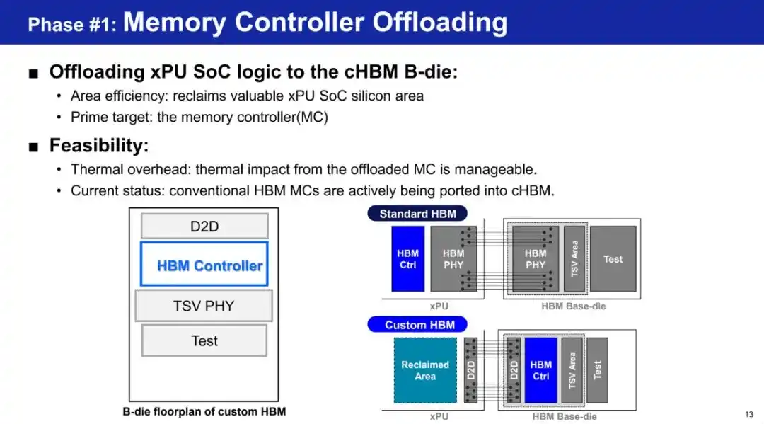
Another major advantage is memory controller offloading, which can be moved from the xPU to the custom base die. This frees up space on the xPU die, which can be used to drive more floating-point processing units.
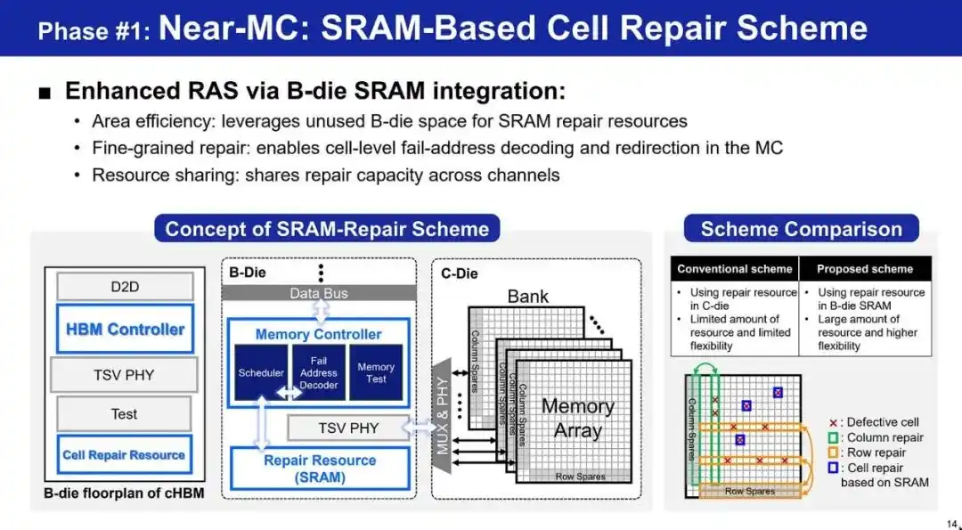
A new advantage of integrating a logic node in the base die is the ability to implement SRAM. If a cell in the DRAM stack is damaged, the information from that cell can be temporarily stored in SRAM, and the memory controller looks it up from the SRAM instead of the damaged DRAM cell. Think of SRAM as a spare notebook—it's like a temporary scratchpad for holding data that can't be stored in the damaged DRAM cell.
Phase 2: RAS, Test, Expansion, Processing
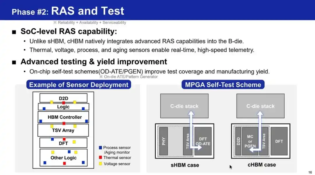
Using a logic node for the base die means that if the transistor size is smaller, the silicon area used for many such functions is also smaller. The saved space can be used for various purposes, such as improving repairability, availability, and serviceability (RAS), conducting tests, and collecting telemetry data on the health/status of the HBM memory stack. Given that HBM telemetry is the second leading cause of training failures, this HBM telemetry will be very useful.
If there is leftover silicon area, you can build another. A memory expansion controller is used to connect another HBM stack behind the first or insert DRAM chips to expand memory.
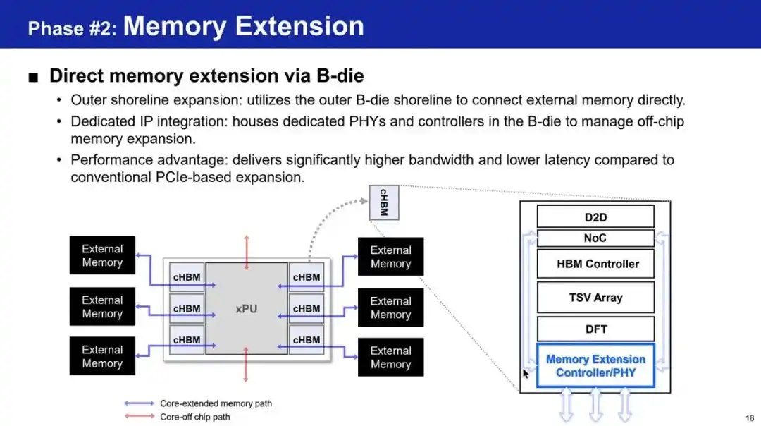
Finally, since logic transistors are available, why not integrate some computing capabilities on the base die as well? The benefit is that computations like matrix compression or encoding can be done on the logic die without leaving the base die. This offers advantages in both latency and efficiency.
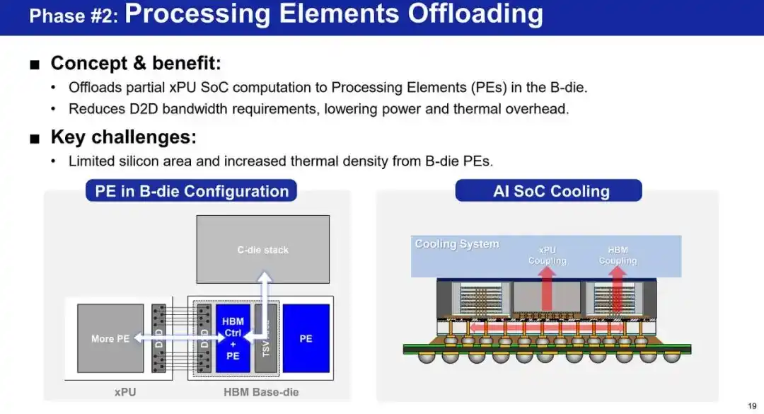
If everything goes well, one could theoretically build the clever accelerator in the lower right corner. Drawing such block diagrams is easy, and the concept is interesting, but whether its actual performance improvement is significant remains questionable.
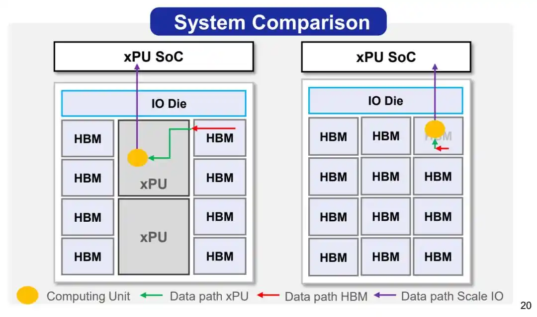
Phase 3: Going Vertical
The final phase is to use the custom base die and HBM and stack them on top of the logic chip. The distance between the compute chip and the memory chip is very short, so data bits only need to travel a shorter distance, improving energy efficiency and increasing memory bandwidth due to the ability to use more parallel data paths across the chip area, not just the chip's edge.
All of this is not easy, but it's crucial for a company to have a roadmap for technological improvements. It shows they are confident in delivering better products in the future, which is good for the company. Whether the market is ready for this product is another question.
SK Hynix Pushes Hybrid Bonding for HBM5
Speaking at Hot Chips 2026 on August 23, Jaesik Lee, Vice President of Package Engineering at SK Hynix America, said SK Hynix expects hybrid bonding will not be ready for HBM4E, pushing the industry's most anticipated memory packaging transition to HBM5 at the earliest.
As he described it, the issue is that the total thickness of the HBM cube is limited to 775 micrometers—the standard thickness for 300mm logic wafers—so each additional DRAM layer requires thinner dies and narrower gaps. The 16-high HBM4, currently undergoing customer validation (with 12-high already in production), thins its core dies to about 50 micrometers and halves the gap between dies. Lee's talk also detailed the company's iHBM cooling architecture, launched three months after its May announcement. Lee explained that a limitation exists in that the thermal module cannot be applied to any HBM products already in design.
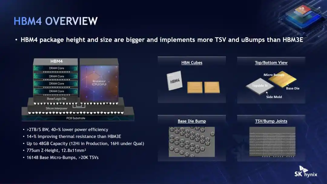
The JEDEC HBM4 standard raised the package thickness limit from the 720 micrometers carried over from HBM3E to 775 micrometers, easing the pressure for adopting hybrid bonding. Lee said that when a GPU package is installed with a cold plate, both the logic chip and the memory stack are ground down, exposing bare silicon. Since logic wafers are 775 micrometers thick, if the memory chip height increases further, it would exceed the processor's height next to it. "This is the limit we can currently push to, because the logic wafer is also 775 micrometers thick," Lee said.
Thinner dies mean a higher proportion of oxide layers in the stack, and oxides conduct heat far less effectively than silicon. Additionally, pin speeds increasing from 1 Gbps in early HBM to 8 Gbps in HBM4 means more power must be dissipated in the same area. SK Hynix's own data shows that thermal load is, on average, 2.2 times higher across the HBM generations shown, while stack height doubles every two generations.
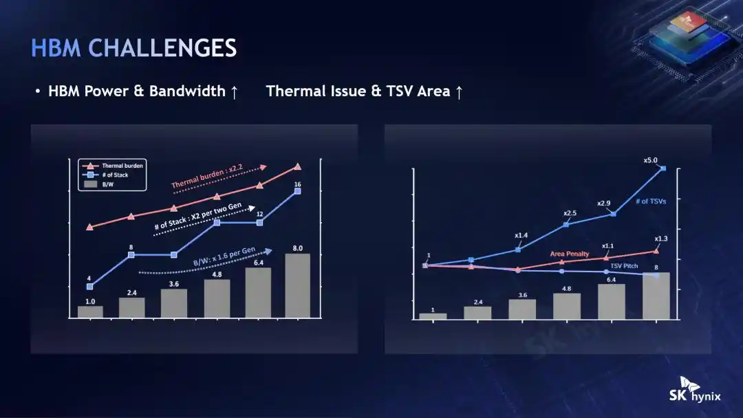
The company's Mass Reflow-Molded Underfill (MR-MUF) process, which stacks all dies via pick-and-place and connects them in a single reflow, has already sacrificed margin: filling the halved gaps while controlling warpage for dies thinner than 50 micrometers is the main manufacturing challenge for 16-Hi, according to Lee.
Last May, Samsung publicly committed to using hybrid bonding for HBM4, while SK Hynix positioned copper-copper bonding as an alternative to advanced MR-MUF. Subsequently, JEDEC relaxed the thickness limit, making hybrid bonding less urgent. Currently, the industry is discussing further increasing the thickness for 20-layer stacks to 825-900 micrometers, which would again delay the widespread adoption of copper bonding.
Back in March, industry sources claimed SK Hynix placed its first large-scale production order for hybrid bonding—a single-line system worth about 200 billion won ($150 million) combining tools from Applied Materials and Besi. Counterpoint Research expects the technology to enter full HBM production around 2029-2030 with the launch of HBM5.
According to SK Hynix's roadmap, hybrid bonding is still in the R&D stage for 20-layer and higher stacks, with SK Hynix still deciding which product will adopt it first. Mr. Lee did not specify which generation, but ruling out HBM4E, HBM5 is likely the earliest candidate. The technology bonds flat copper pads and oxide surfaces at room temperature, then uses copper's thermal expansion during curing to form the bond.
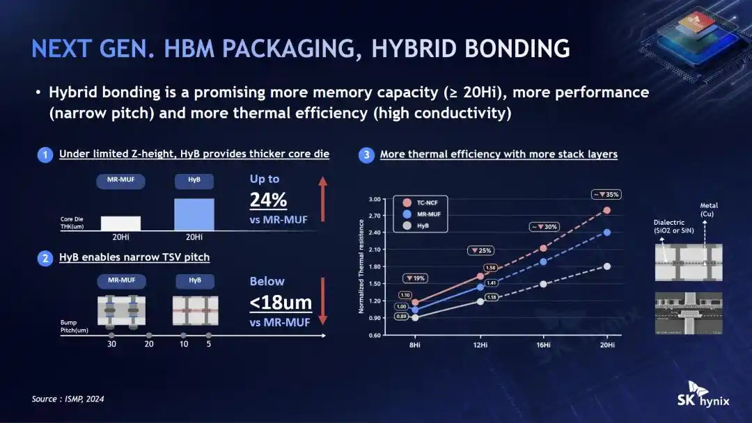
"It seems simple, but it's very challenging," Lee said. "We need 16 or even 20 layers to enable hybrid bonding, which is different from single-layer stacking." Completely removing microbumps allows core dies to be 24% thicker at 20-high, reducing thermal resistance by about 35% compared to MR-MUF at the same height, and bump pitch (according to the die layer diagram) can be below 18 micrometers, versus MR-MUF's current 30 micrometers. At HBM4 bump pitches, traditional microbumps remain sufficient, and each time JEDEC raises the thickness limit, MR-MUF remains viable and extends to the next generation.
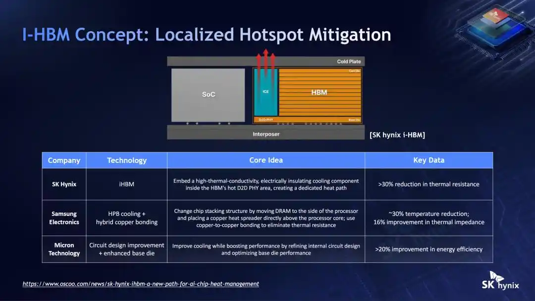
The iHBM concept embeds thermally conductive, insulating blocks into the inter-die PHY area of the base die (the interface hotspot of peak power density), reportedly reducing thermal resistance by over 30%.
Lee's slide directly compared iHBM with Samsung's Heat Path Block solution and Micron's base die circuit redesign claiming over 20% power efficiency improvement. All three are vendor claims with different metrics. Both SK Hynix's and Samsung's designs are planned for HBM5 but are not expected to enter volume production before 2028. Lee said that because these modules are located inside the package along with the D2D PHY die, they need to be optimized for customer designs and cannot be applied to already-designed chip generations, making iHBM a co-design effort. "It's a nice option we can do, but we cannot apply it to chip generations we have already designed."
During the Q&A, Tanj Bennett from SemiAnalysis pointed out that stacking memory higher reduces the silicon's own throughput. DRAM, operating at the cell level, offers about 20 TB/s per square centimeter; whereas a 20-high stack tops out at around 4 TB/s, and HBM requires significantly more manufacturing capacity than equivalent DDR5 or LPDDR. "When you get to 20-high, this memory is slower on average than DDR5," Bennett said. "Why not utilize the height of HBM stacking instead of cleverly placing cheaper memory around it?"
Lee replied that training workloads require both bandwidth and capacity, then added that inference can accommodate both by keeping key-value caches in high-bandwidth memory while offloading part of the work to LPDDR memory. This disaggregation is already being used in products like NVIDIA's Vera Rubin platform, which pools LPDDR5X and HBM4 via NVLink-C2C for this purpose. Furthermore, the High-Bandwidth Flash specification co-developed by SK Hynix and SanDisk extends this hierarchical concept to NAND flash.
Speaking about the tiering approach, Lee said, "This is also something we need to consider for the future." According to a January report, SK Hynix secured about 70% of NVIDIA's HBM chip orders for the Vera Rubin generation, all using MR-MUF. Lee said the company has not yet decided which product will first adopt MR-MUF.
Micron Sees the 'Memory Wall' Worsening
In its presentation, Micron Technology will explore the evolving memory architecture in the AI field. It is understood that Micron will detail how High Bandwidth Memory and advanced packaging technologies have become central to AI system design.
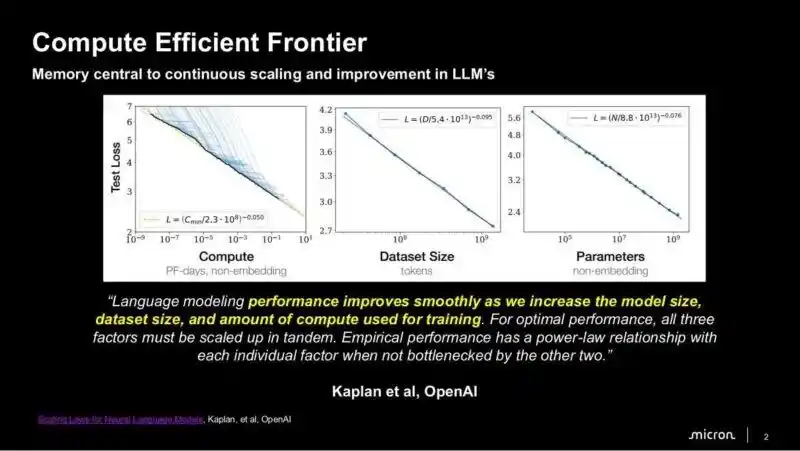
Micron's talk opened with OpenAI's compute efficiency frontier theory, explaining why memory is crucial for scaling language models. Micron pointed out a power-law relationship between model size, dataset size, and training compute, arguing that all three must scale together to improve language model performance. Memory is the key resource linking these three factors.
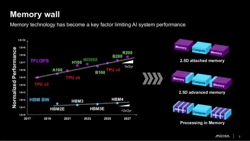
Now let's talk about the memory bottleneck. Micron stated that AI accelerator TFLOPS (floating-point performance) grows roughly 3x every two years, while the bandwidth of 2.5D attached memory (e.g., HBM) grows at less than 2x every two years. This widening gap is why memory technology has become a key limiting factor for AI system performance.
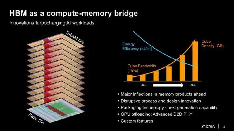
Micron positions HBM as a bridge between compute and memory, tracking the increasing capacity, bandwidth, and energy efficiency from HBM2e to HBM5 generations. You have to appreciate a tech conference presentation without a labeled Y-axis.
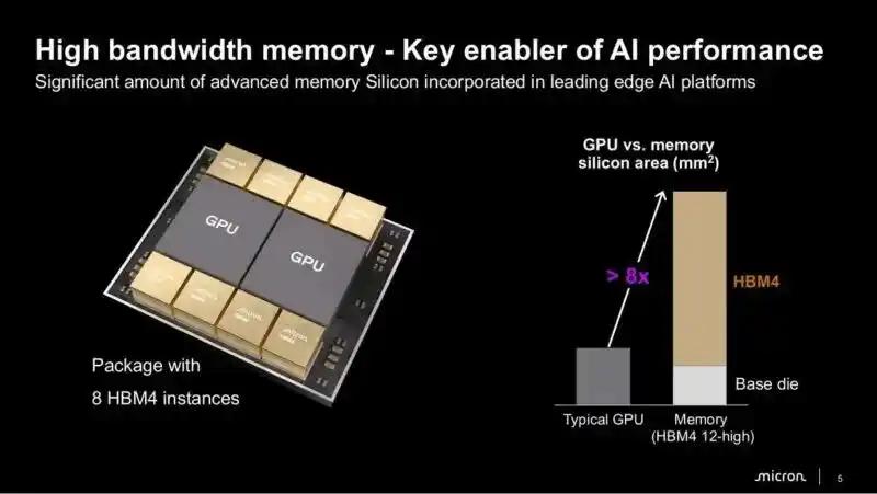
Here, Micron showed a typical GPU with a package area exceeding 12,000 square millimeters, including the base die and eight HBM4 instances. This means that with 12-high HBM4, the memory silicon area can be over 8 times the area of the GPU die itself. That's indeed a very visual demonstration.
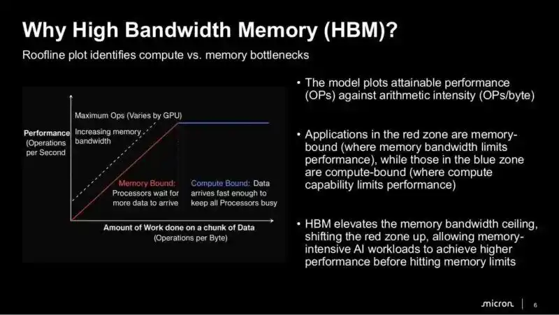
HBM raises the memory bandwidth ceiling, shifting the boundaries of memory limitations, allowing memory-intensive AI workloads to run faster before hitting memory constraints.
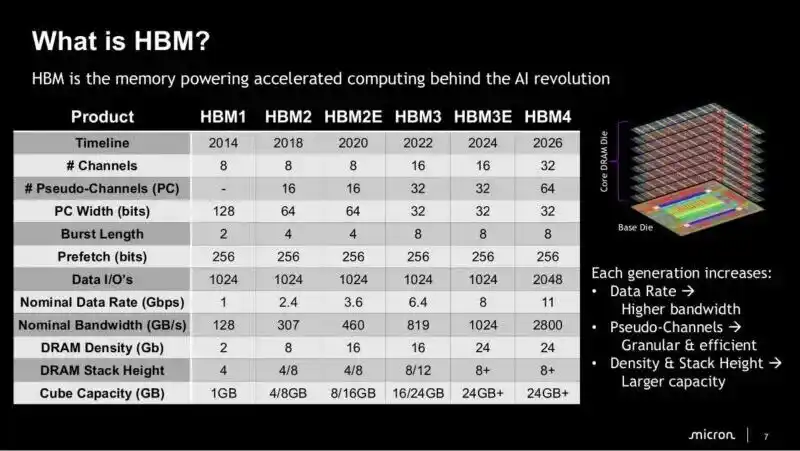
Micron's presentation is now detailing what HBM is and the evolution across generations. A product table shows the progression from HBM1 to HBM4. Each generation increased data rate, pseudo-channel count, and stack height, providing higher bandwidth and greater capacity.
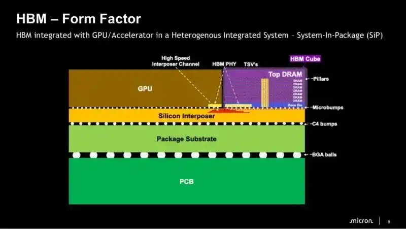
HBM is mounted differently from a standard JEDEC RDIMM. The diagram below shows how an HBM stack integrates with a GPU or accelerator in a heterogeneous integration system and is packaged as a System-in-Package (SiP), not as a separate slot module. I think many at STH have seen this design before.
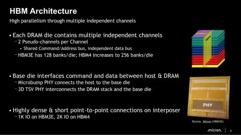
Each DRAM die contains multiple independent channels, each with two pseudo-channels; HBM3E carries 128 banks per die, while HBM4 doubles this to 256. The base die sits between the host and the DRAM stack, with a microbump PHY on the host side and a 3D TSV PHY on the stack side, connected via a high-density point-to-point interposer, increasing from 1K IOs in HBM3E to 2K IOs in HBM4.
Micron is now showing the trade-off between performance and capacity. But they aren't really showing the differences in PCB area and power consumption here. Maybe that will come in a later slide?
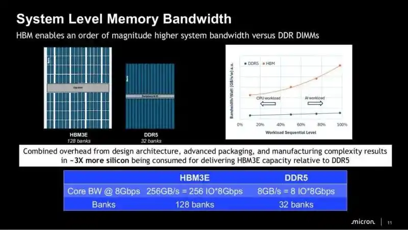
Micron now notes the silicon cost of this speed. The combined costs of design architecture, advanced packaging, and manufacturing process complexity mean that achieving the same capacity as DDR5 with HBM3E requires about three times more silicon.
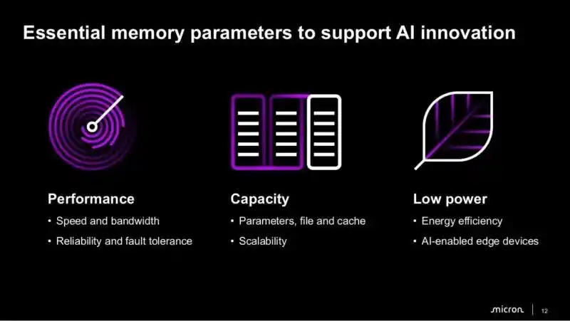
Micron then summarized in its talk the memory parameters supporting AI innovation, including performance, capacity, and power consumption.
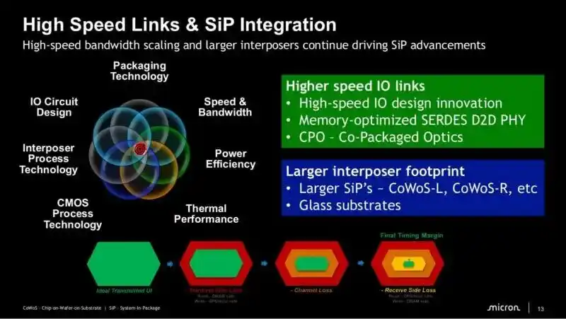
Higher-speed I/O links and larger interposers continue to drive SiP advancements, including faster I/O designs, memory-optimized SERDES and inter-die PHY, and co-packaged optics on the interconnect side. Larger SiPs based on technologies like CoWoS-L and CoWoS-R, as well as glass substrates, are also part of the packaging roadmap.
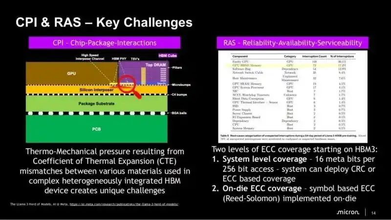
Now let's talk about reliability, including chip-package interaction and RAS challenges. In heterogeneous integrated HBM devices, coefficient of thermal expansion mismatches between different materials create thermomechanical stress. In fact, from a broader perspective, this was one of the biggest challenges faced during the implementation of Cerebras's WSE. ECC coverage is divided into two layers: first, HBM3, which uses 16 meta-bits per 256-bit access at the system level; and second, symbol-based Reed-Solomon ECC implemented on-chip.
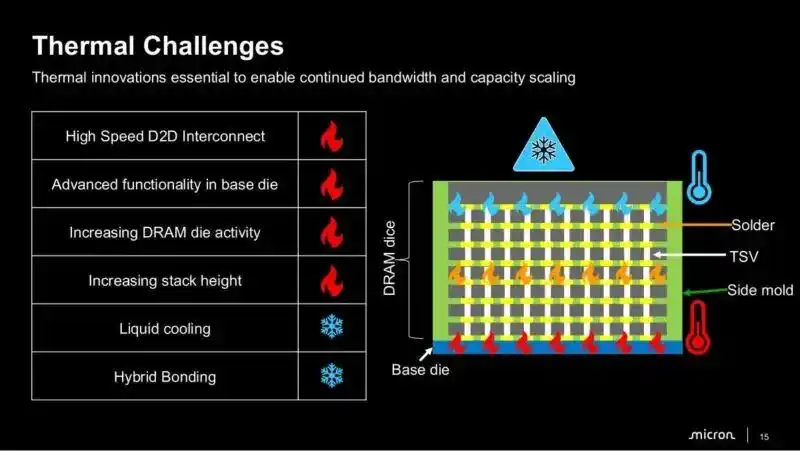
To manage heat, increased DRAM die activity, higher stack heights, and more advanced base die functionality all contribute to increased heat generation. Micron noted that liquid cooling, hybrid bonding, and improvements in solder and side molding are thermal innovations needed to sustain the bandwidth and capacity scaling.
The packaging trend seems to be nearing its end.
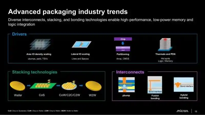
Overall, this data indicates how Micron Technology is navigating the evolution of memory architecture in the AI field. Micron is weighing the benefits of increasing HBM bandwidth and capacity against the packaging, thermal, and reliability costs of placing such large memory capacities next to compute units.
What do you think about the future direction of HBM?
This article is from the WeChat public account "Semiconductor Industry Watch" (ID: icbank), by the Editorial Department.