Core Scientific Writes Off $41.9 Million to Accelerate Exit from Bitcoin Mining
Core Scientific reported a $41.9 million payment to terminate a contract with Block and its subsidiary Proto for the supply of Bitcoin mining chips. This move finalizes its exit from plans to grow its hash rate, shifting its business model entirely towards AI colocation.
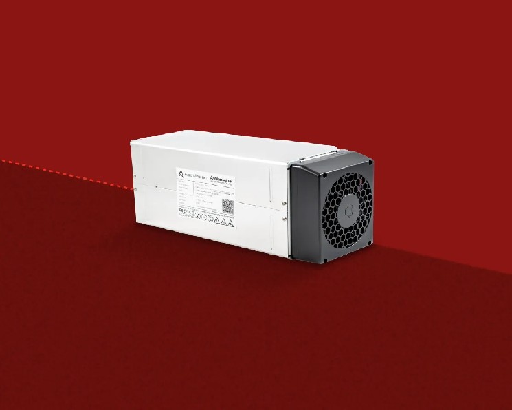
The agreement, announced in July 2024, was for 3nm chips providing roughly 15 EH/s of hash rate. Following the cancellation, Core Scientific stated it will no longer invest in new mining hardware to maintain or expand its cryptocurrency mining capacity. Instead, it will generate cash flow from its existing mining fleet while repurposing its data centers, potentially selling or decommissioning ASIC miners.
In Q2 2026, revenue from AI colocation surged to $136.7 million from $10.6 million a year earlier, representing 83% of total revenue. In contrast, its own Bitcoin mining revenue fell 66% to $21.5 million. Quarterly Bitcoin production dropped 53% year-over-year.
AI colocation capacity reached 437 MW by mid-July 2026, with CoreWeave accounting for all current hosting revenue and approximately 77% of Core Scientific's total revenue in H1 2026. The company also announced a partnership with AMD for up to 2.5 GW of potential data center capacity, with initial 15-year agreements for about 530 MW estimated to bring in over $14 billion in contract revenue.
Total Q2 revenue grew to $164.2 million, while capital expenditures jumped to $797.5 million. As of June 30, 2026, the company reported long-term debt of $4.3 billion and free liquidity of $1.82 billion. The shift aligns with a broader industry trend of major Bitcoin miners accelerating a pivot to AI amid pressure on Bitcoin mining profitability.
cryptonews.ruHá 31m