TL;DR
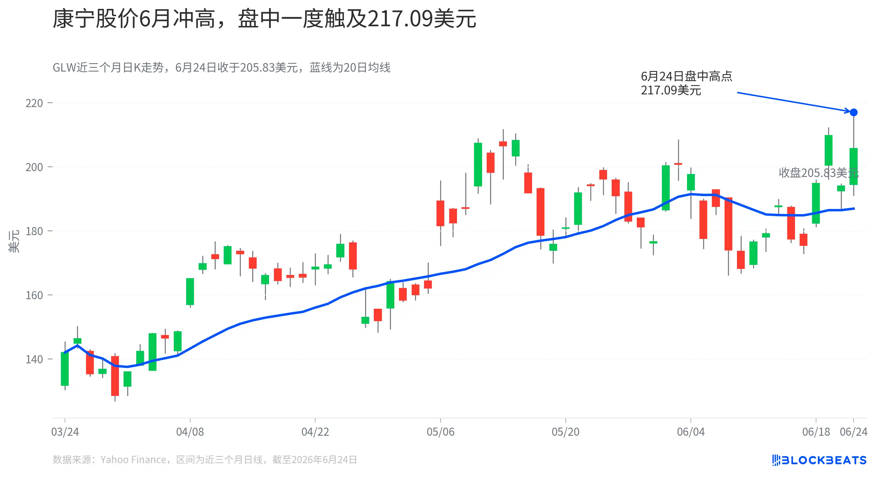
Corning's stock price is already at a high level. As of the close of U.S. trading on June 24, Corning (GLW) closed at $205.83, up about 6.1% for the day, with an intraday high of $217.09. The demand for AI data center optical interconnect is one of the core reasons the market is reassessing this established glass and fiber optics company.
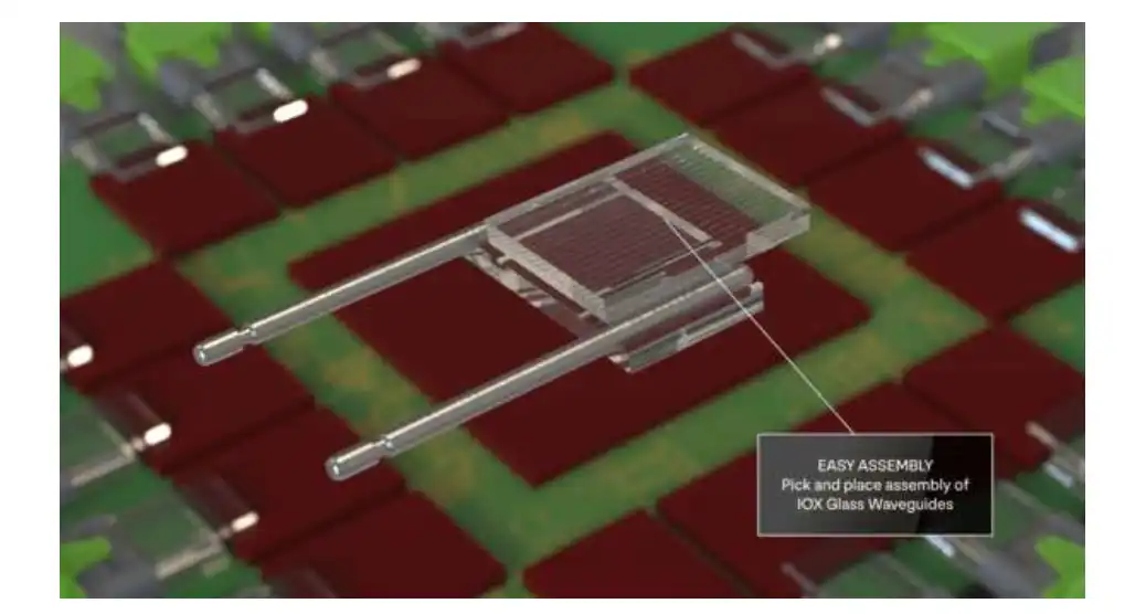
According to materials from the Seoul AI Data Center Optical Communication Conference on June 24, Corning showcased the GlassBridge glass-based optical bridge, attempting to advance fiber connections to near the photonic integrated circuit. Corning's official product page positions it as a "fiber-to-PIC connector platform" for scenarios like NPO, CPO, and high-density photonic modules.
It belongs to optical interconnect components that are closer to the chip, positioned deeper than traditional pluggable optical modules. As AI data center GPU clusters grow larger, the pressure of data movement between chips, servers, and racks increases. Electrical connections and traditional optical connections face bottlenecks in density, power consumption, latency, and assembly complexity. CPO, or Co-Packaged Optics, aims to address precisely this issue of pushing optical connections closer to the chip.
A key aspect of Corning's recent highlighting of GlassBridge is advancing the company's long-accumulated expertise in glass and fiber optics into the chip-level packaging and interconnect domain. Public documentation states that this platform, based on glass and wafer-level IOX ion-exchange waveguides, has demonstrated O-band fiber-to-photonic chip coupling performance of 1.5 dB, and supports passive alignment, detachability, and high-density connections.
The Glass Bridge Aims to Solve the "Misalignment" Between Fiber and Chip
Optical interconnect might sound like simply attaching an optical fiber to a chip, but the real challenge lies in the scale difference.
Waveguides on a photonic chip are typically only a few hundred nanometers wide, while the core diameter of an optical fiber is on the order of several micrometers. When signals travel from the fiber into the photonic chip, any deviation in the optical path, angle, or position introduces coupling loss. For high-density AI servers, this simultaneously impacts link efficiency, assembly, testing, and packaging difficulty.
GlassBridge's approach involves pre-forming optical pathways in glass to guide fiber signals to the photonic chip interface. Public documentation lists customizable PIC pitches including 40μm, 80μm, 127μm, and 165μm diameters. Compared to directly aligning a fiber array to the chip, this type of glass bridge aims to reduce assembly difficulty and eliminate some intermediate connection stages.
The 1.5 dB figure is the most notable performance metric highlighted this time, but it should still be understood as a demonstration figure from public documentation, not equivalent to having passed large-scale mass production validation. Before entering real data centers, this component must still undergo validation for packaging yield, long-term reliability, thermal stability, and ease of maintenance.
The Closer CPO Gets to the Chip, the Higher the Packaging Difficulty
CPO is valued by AI data centers because it has the potential to reduce the power consumption and latency of high-bandwidth interconnects. In traditional network connections, optical modules are typically plugged into switch or server panels, requiring electrical signals to travel a distance between the chip and the module. As the bandwidth demands of AI clusters continue to rise, this electrical connection becomes more costly and power-hungry.
Integrating optical devices into the package or near the chip can theoretically shorten the signal path and increase bandwidth density. However, the closer to the chip, the less the technical difficulty resembles that of ordinary optical modules and the more it resembles advanced packaging engineering. Photoelectric conversion, fiber coupling, thermal management, packaging materials, assembly precision, and manufacturability all have to be addressed within the same system.
Corning's showcased next-generation CPO glass-based architecture integrates glass substrates, optical waveguides, and through-glass vias (TGV) into a single concept and supports flip-chip mounting of photonic devices. The key change is that Corning is attempting to advance glass from a transmission material to a packaging platform position.
This also explains why GlassBridge appears alongside glass-core packaging. Glass materials offer advantages in dimensional stability, optical properties, and processability, making them suitable for carrying high-density optical pathways. However, the ultimate adoption of advanced packaging still depends on mass production yield, cost curves, supply chain equipment, and customer validation cycles.
Corning Wants to Sell an Optical Interconnect Solution
GlassBridge sits within Corning's broader AI data center optical communication strategy. In its OFC 2026 press release, Corning already showcased optical fibers, cables, connectors, and CPO-related solutions for AI data centers. The GlassWorks AI platform integrates optical fibers, cables, connectors, Fiber Array Units (FAU), and alignment components into a comprehensive AI data center optical communication solution, covering inter-rack and campus-wide connections.
This reflects Corning's evolving position within AI infrastructure from a "fiber and cable supplier" to an optical interconnect supplier moving closer to the system's interior. AI data center construction is driving up demand for optical fibers, connectors, and high-speed interconnects, while CPO and glass-core packaging are pushing demand even closer to the chip.
Customer and capacity plans are the foundation for Corning's advancement on this path. Corning is collaborating with GlobalFoundries on the GF Fotonix platform to develop detachable fiber connectivity solutions targeting high-bandwidth, low-power optical connections for AI data centers. The company has also signed a multi-year agreement with Meta worth up to $6 billion and announced a long-term commercial and technical collaboration with NVIDIA, involving the expansion of U.S. AI infrastructure manufacturing capacity.
However, this context cannot be directly equated with GlassBridge having secured large-scale deployment orders. The current materials do not disclose the component's mass production timeline, final yield, customer list, revenue contribution, or a clear timeline for integration into which generation of switch chips, AI servers, or packaging platforms.
For the Glass Route to Move Forward, It Still Awaits Customer Platform Validation
Corning is now presenting the intersection of glass materials, fiber connectivity, and advanced packaging to the AI data center market. If GlassBridge can achieve low loss, easy assembly, and manufacturability simultaneously in high-density interconnects, it could become a key component within CPO packaging.
The limitations are clear. Current public information points more towards a product platform and technology demonstration; the mass production timeline, yield, cost competitiveness, and major customer deployment cadence have not been disclosed. Route competition is also not over, with AI data center optical interconnects still seeing parallel advancement of multiple schemes including silicon photonics, glass-based packaging, and hybrid interconnect architectures.
The final choice of route by cloud providers and chipmakers will depend simultaneously on individual coupling loss metrics, overall system design, power budgets, supply chain stability, and maintainability. GlassBridge appears more like a step by Corning into AI chip-level optical interconnect; glass-based CPO still requires more customer validation before it can be considered a winning solution.