Edited & Compiled: Deep Tide TechFlow
Host: Nico
Original Title: AI Optical Interconnect: The Next Trillion-Dollar Track Hidden by GPU's Glare?
Podcast Source: Nico Frontier Alpha
Broadcast Date: May 8, 2026
Editor's Introduction
Optical interconnects are transforming from "supporting components" for GPUs into a core bottleneck for AI data centers. When single cabinets, cross-cabinet connections, and even super nodes require hundreds or thousands of GPUs to work in coordination, what truly determines computing power utilization is no longer just the chips themselves, but the data transmission capability between GPUs.
This episode, from an industry chain investment research perspective, weaves optical modules, silicon photonics PICs, CPO, external laser sources, InP substrates, SOI substrates, foundries, and packaging & testing into one map, and provides a hierarchical allocation framework from AVGO, MRVL, GLW to COHR, LITE, TSEM, and then to SIVE, AAOI, AXTI, IQE, Soitec.
The most valuable part of this content is not a single stock recommendation, but an assertion: the competition in AI infrastructure is extending from "who has more GPUs" to "who can lock down the more scarce optical interconnect supply chain," with CPO (Co-Packaged Optics) possibly being the biggest incremental variable within it.
Key Quotes
Why Optical Interconnect Suddenly Matters
- “Even if an NVIDIA GB300 GPU accelerator card has incredibly strong computing power, if it cannot communicate at high speed with thousands of other GPUs, most of its computing power is wasted.”
- “If interconnect bandwidth isn't sufficient, spending more money on GPUs yields diminishing returns.”
- “Whether it's training or inference, as long as it involves collaborative work, GPUs must exchange data at high speeds. This data pathway is the interconnect.”
- “Optical interconnect is not hype. The interconnect demand in AI data centers is real, urgent, and irreversible.”
The Retreat of Copper Cables and the Rise of Fiber Optics
- “The transmission speed of copper cables is nearing its physical limit; the bandwidth a single copper wire can carry is maxed out.”
- “Beyond a few meters, copper cables start to experience signal attenuation and interference, but the connection distances in AI data centers can easily reach tens or hundreds of meters.”
- “The bandwidth of a single optical fiber is dozens of times that of copper cables, capable of transmitting data over several kilometers without issues, and its energy consumption is negligible.”
The Industrial Nature of Optical Modules
- “Optical modules are responsible for communication *between* different cabinets, not for communication between GPUs *within* a single cabinet.”
- “The optical module industry chain and the GPU industry chain are not two separate tracks; GPU shipment volume directly drives optical module demand.”
- “The manufacturing of an optical module spans two entirely different semiconductor process systems: InP compound semiconductors for the optical chips, and silicon for the DSP chips.”
The True Significance of CPO
- “CPO doesn't disrupt a single component within the optical module; it disrupts the product form of the optical module itself.”
- “CPO is not an upgrade or replacement for existing products; it is an architectural-level reconstruction.”
- “A more accurate relationship is that CPO opens up a brand new market that is potentially much larger than the pluggable optical module market, rather than simply replacing the existing market.”
Industry Chain Investment Framework
- “The optical interconnect industry chain is not like GPUs, dominated by a single player like NVIDIA. It is an industry chain with extremely fine division of labor and highly scattered bottlenecks.”
- “The further upstream you go, the smaller the companies, the greater the potential upside, but the lower the certainty. The further downstream you go, the larger the companies, the higher the certainty, but the smaller the upside.”
- “If you can tolerate high risk and high volatility, the core logic is to target the bottlenecks. Behind each bottleneck link, there is often only one or two companies capable of handling it.”
The "Neural Network" of AI Infrastructure, Truly Scarce Beyond GPUs
Over the past two to three years, almost everyone has been discussing GPUs and computing power. Since ChatGPT (the generative AI product launched by OpenAI that ignited the large model application wave) was born and the AI tech revolution exploded, NVIDIA's stock price has multiplied by 15 times in three years, and computing power has become an unavoidable keyword for AI large models. The semiconductor industry chain, centered on GPUs, has also entered a golden age transcending economic cycles.
However, over the past year, a link as crucial as, or even more scarce than, GPUs has quietly exploded. In large-scale data center deployments, even if a single NVIDIA GB300 GPU accelerator card is incredibly powerful, if it cannot communicate at high speed with thousands of other GPUs, most of its computing power will be wasted. Without sufficient interconnect bandwidth, buying more GPUs yields diminishing returns. This link, responsible for enabling high-speed communication among thousands of GPUs, is optical interconnect.
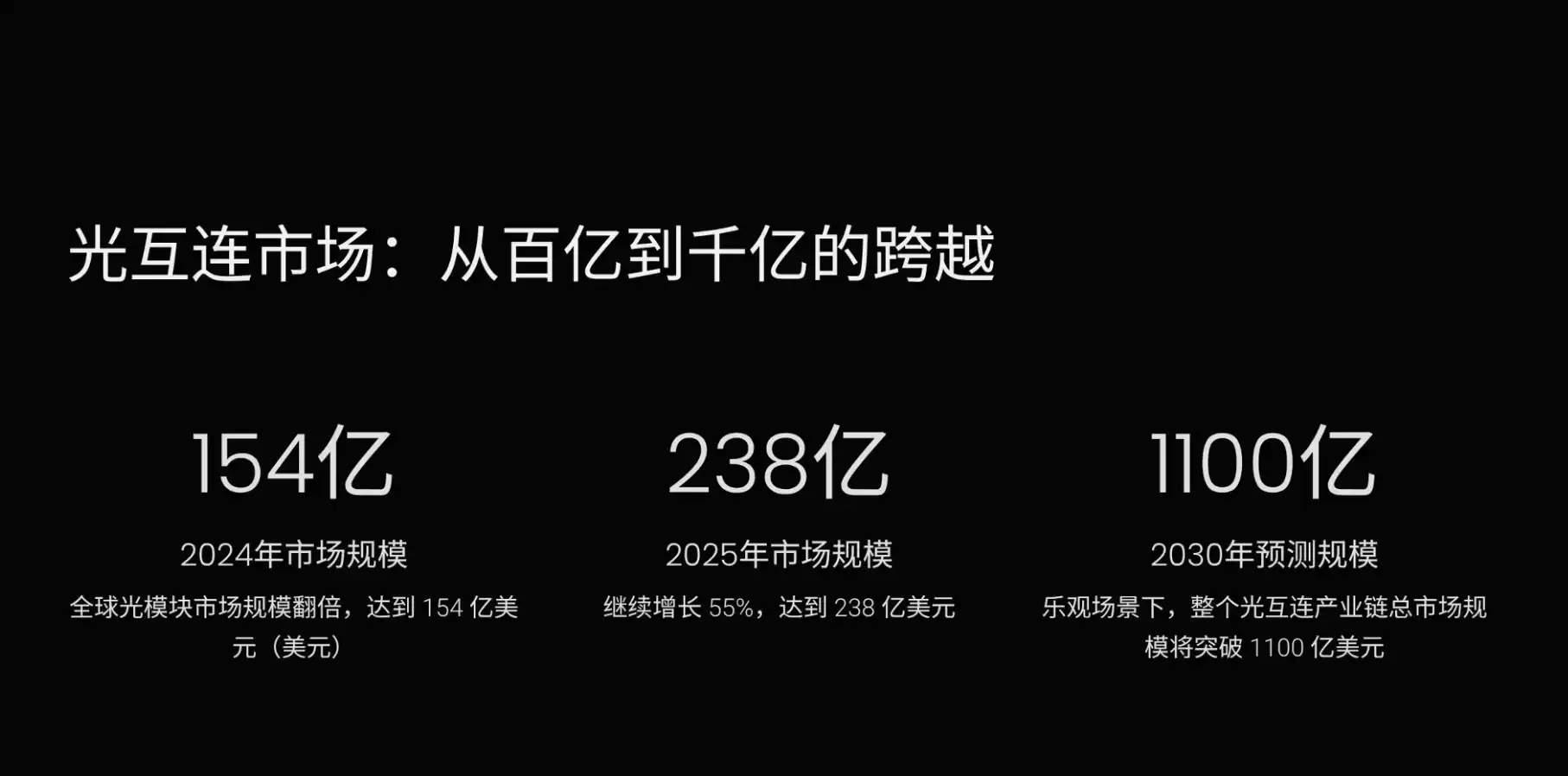
According to data from LightCounting (a research firm in the optical communication field), the global optical module market doubled in size in 2024, reaching $15.4 billion; it grew another 55% in 2025, reaching $23.8 billion. In an optimistic scenario, LightCounting predicts the total market size of the entire optical interconnect industry chain will exceed $110 billion by 2030.
Yet most investors probably haven't even heard the names of the companies on this industry chain. SIVE/SIVEE has annual revenue of around $30 million, and its stock has surged 10-fold since the beginning of 2026. TSEM (Tower Semiconductor, an Israeli specialty foundry) is called the "TSMC of optical interconnects" by the market, with 70% of its capacity booked through 2028. COHR (Coherent, a vertically integrated company in optics and materials) has annual revenue of about $5.8 billion and received a $2 billion strategic investment from NVIDIA.
Today's episode will dissect this optical interconnect industry chain from start to finish. What is optical interconnect, what's inside an optical module, what's the next-generation technology roadmap, where are the key bottlenecks in the industry chain, what position does each company occupy, and how investors can allocate to this track according to their own risk preferences.
Training, Inference, and Interconnect: Why GPUs Must Communicate at High Speed
Before discussing specific companies, we need to explain a question: why has optical interconnect suddenly become one of the most critical and scarce links in AI infrastructure? It starts with understanding how AI works. AI work is divided into two stages: training and inference.
Training involves feeding large amounts of text, images, code, etc., to a model, allowing the model to continuously learn and evolve based on the provided content. The training parameters for a large model may reach trillions, which no single GPU can accommodate. Therefore, it must be split into thousands of parts and distributed across thousands of GPUs for parallel computing. After each GPU calculates its assigned portion, it must transmit the intermediate results to other GPUs for collaborative completion of the entire task.
Inference is when the AI uses learned knowledge to produce answers. You ask ChatGPT a question, and it responds tens of seconds later—that's inference. Many people think inference is just one GPU answering one question, with no need for interconnect. That might have been somewhat true in 2023, but by 2026, it's completely different.
AI has evolved from simple Q&A to deep reasoning and Agentic AI. The user interaction object is no longer just a simple chatbot but a complex Agent (intelligent agent) that may need to plan tasks, perform multi-step reasoning, and query multiple data sources. Behind each interaction, hundreds or even thousands of GPUs might be working in coordination. Whether it's training or inference, as long as collaborative work is involved, GPUs must exchange data at high speed. This data pathway is the interconnect.
Why Copper Cables Are No Longer Sufficient
In the past, interconnects primarily used copper cables, transmitting electrical signals. Now, this pathway is gradually being replaced by optical fibers, transmitting light signals. Copper cables are insufficient for three main reasons.
First, copper cable transmission speed is nearing its physical limit. No matter how much you optimize materials and processes, the bandwidth a single copper wire can carry has reached its ceiling. It's like a congested two-lane highway—you can only have two cars running side-by-side. Second, signal degrades with distance. Copper cables start to attenuate and experience interference beyond a few meters, while connection distances in AI data centers can easily reach tens or hundreds of meters; copper cables can't handle it. Third, copper cables consume more power. GPU power consumption rises with each generation: H100 is 700 watts, B200 is upgraded to 1 kilowatt, and GB300 will be even higher. At these power levels, the copper cable connections between GPUs themselves can consume significant electricity.
Optical fibers are entirely different. The bandwidth of a single fiber can be dozens of times that of copper cables, capable of transmitting data over several kilometers without issues, with negligible energy consumption. Fibers can also simultaneously transmit multiple light signals of different wavelengths, like dividing a highway into 8 lanes, each carrying light of a different color without interfering with each other. One fiber can effectively replace dozens of copper cables.
The Three Stages of Optical Interconnect
The use of optics in data centers is not something new that suddenly appeared; it has gone through several very clear stages. In each stage, the coverage of optics is moving closer to the chips.
The first stage was before 2020. Back then, optics were mostly used *between* data centers—for example, a cloud provider having a data center in Beijing and another in Shanghai, separated by over a thousand kilometers, requiring fiber optic connections. However, inside the data centers, connections between servers mostly still used copper cables.
The second stage was 2023 to 2024. ChatGPT ignited the AI tech revolution at the end of 2022, and GPUs sold like crazy the following year. But the optical module market didn't significantly take off initially. The reason was that NVIDIA GPU clusters mainly still used copper cables back then; optical modules were not core components. Worse, at the beginning of 2023, cloud providers slashed capital expenditures due to recession fears, with Meta (Facebook's parent company, a major global cloud and AI infrastructure buyer) even cutting more than half of its optical module deployment plans.
The real turning point came in 2024. Cloud providers' GPU clusters expanded from hundreds to thousands, even tens of thousands of GPUs. Copper cables' transmission range of just a few meters completely collapsed. NVIDIA replaced copper cables with pluggable optical modules in its reference architecture. This architectural-level switch ignited the market, causing the optical module market to double in size in 2024.
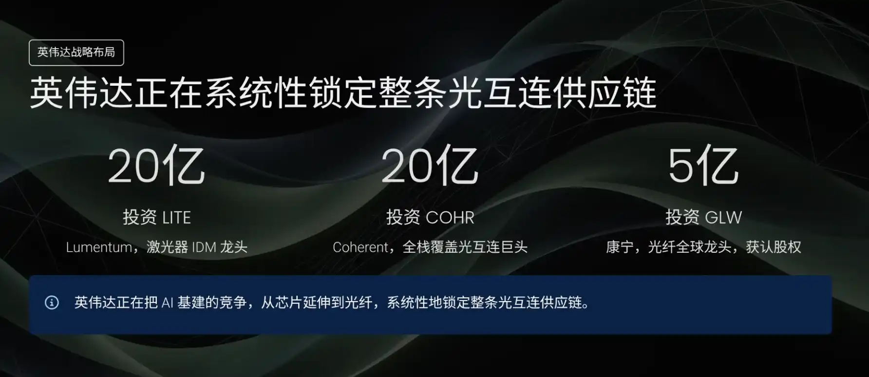
The third stage is from 2025 to the present. NVIDIA Blackwell (NVIDIA's next-generation AI GPU architecture) began large-scale deployment, with higher power consumption and greater interconnect bandwidth demands, further exploding demand for optical modules. At the same time, the combined capital expenditures of the five major cloud providers for the first nine months exceeded $300 billion, hitting a record high. Optical module demand at one point exceeded supply by more than twofold, leading to a severe supply-demand imbalance. In March of this year, NVIDIA invested another $2 billion each in Lumentum and Coherent. At GTC 2026 (NVIDIA's annual developer conference), NVIDIA showcased its CPO solution and the optical interconnect design for the next-generation Rubin architecture, essentially declaring that optical interconnect has moved from a niche track to the main narrative of AI infrastructure.
What is an Optical Module: The Translator Between Electrical and Optical Signals
Before getting into the investment research content, we need to explain a few basic concepts. The first is the optical module. The GPU chip itself only recognizes electrical signals, while optical fibers carry light signals. The two languages differ, requiring a translator to convert electrical signals into optical signals for transmission, and upon receiving optical signals, translate them back into electrical signals. This translator is the pluggable optical module.
An optical module is about the size of a USB flash drive, with one end plugged into a server network card and the other connected to an optical fiber. In a large AI data center, there might be tens of thousands, even hundreds of thousands, of these "little boxes." Here's a concept easily misunderstood: optical modules are responsible for communication *between different cabinets*, not for communication *between GPUs within the same cabinet*.
Taking the NVIDIA GB300 NVL72 (NVIDIA's rack-level GPU system) as an example, a single cabinet contains 72 GPUs. Communication between these GPUs uses NVLink and NVSwitch (NVIDIA's high-speed GPU interconnect technology and switch chips), all via copper wires carrying electrical signals, over distances of only tens of centimeters to one or two meters, requiring no optics. Only when data needs to travel from one cabinet to another, over distances of tens of meters or more, are optical modules required.
In a complete AI cluster, optical modules are typically plugged into two places: server network cards and switches. Each fiber needs an optical module plugged into both ends. More GPUs, more cabinets, and greater connection needs between cabinets drive greater demand for optical modules. The optical module industry chain and the GPU industry chain are not independent tracks; GPU shipment volume directly drives optical module demand.
The Five Core Components of an Optical Module
Inside an optical module, about the size of a USB flash drive, there are typically five core components: the laser chip, modulator chip, detector chip, DSP chip, and lenses/fiber coupling assembly.
First is the laser chip. Its function is to emit light—a stable, continuous laser beam serving as the carrier for the optical signal. A laser chip is like a miniature flashlight, smaller than a fingernail, but emits very precise and pure light. The most critical aspect of the laser is the material. GPUs and CPUs use silicon, whereas lasers use Indium Phosphide (InP) or Gallium Arsenide (GaAs). Silicon inherently doesn't emit light well. Compound semiconductors like InP and GaAs have atomic structures more suitable for generating photons, which explains why laser chips aren't made by silicon foundries like TSMC.
Second is the modulator chip. The light emitted by the laser itself doesn't carry information; it's just a "blank light." The modulator's function is to write electrical signals onto the light. The GPU transmits binary electrical signals (0s and 1s). The modulator controls the laser's on/off state or intensity to represent 0s and 1s with light. Continuing the analogy, the laser is the continuously shining flashlight, and the modulator is the hand controlling the flashlight switch, toggling it hundreds of billions of times per second. Sometimes, the modulator and laser are on the same chip, called an EML (Electro-absorption Modulated Laser), essentially combining the flashlight and switch into one component.
Third is the detector chip. The modulator is responsible for converting electrical signals to optical signals (the sending process). The receiving end needs to convert optical signals back to electrical signals, which requires a detector. It acts like the ear at the receiving end, outputting a 1 when it sees light and a 0 when it doesn't. Detectors also typically use InP or GaAs material systems.
Fourth is the DSP chip (Digital Signal Processor). It acts as the brain of the optical module, responsible for error correction, encoding, and equalizing signal quality. During optical signal transmission, there can be noise and distortion, like trying to hear someone on the phone in a noisy traffic-filled street. The DSP uses special methods to encode at the transmitting end and cleans up noise at the receiving end, ensuring the recovered 0s and 1s match the original data. The DSP is a silicon-based chip, part of the same semiconductor process system as GPUs and CPUs, and is typically manufactured by silicon foundries like TSMC.
800G and 1.6T refer to the transmission speed of the optical module. 800G is 800 Gigabits per second, and 1.6T is 1.6 Terabits per second, doubling the speed. As optical modules progress from 400G to the current mainstream 800G and the now-deploying 1.6T, faster speeds increase chip design difficulty, raising the cost and design complexity of the DSP, sometimes making it more expensive than the laser itself.
Fifth is the lens and fiber coupling assembly. Its job is to precisely align the laser beam to the entrance of the optical fiber. The laser emits a very thin beam, and the fiber core is also extremely thin—about one-tenth the diameter of a human hair—requiring micron-level alignment accuracy. Imagine threading a needle into another needle's eye, but automatically completing this millions of times on a factory production line.
Stringing these five components together, the workflow of an optical module becomes clear. The GPU transmits an electrical signal, which first goes into the DSP for encoding/error correction, then to the modulator. The modulator writes the electrical signal onto the light emitted by the laser. The light enters the fiber through the lens, traveling tens to hundreds of meters. Upon reaching the other end, the light exits the fiber and is aligned by a lens to the detector. The detector converts the light back into an electrical signal, which is then passed to the DSP on that end for decoding/error correction, and finally delivered to another GPU.
How Optical Modules Are Made: Two Semiconductor Process Systems Coexist
Many people subconsciously think, aren't chips made by TSMC? The chips in optical modules should be similar. But the reality is completely different. There are two entirely different types of chips inside an optical module, corresponding to two completely different materials, manufactured in two different types of factories.
The first type is the DSP chip, the brain of the optical module responsible for error correction and encoding. It's a silicon-based chip, using a manufacturing process similar to GPUs and CPUs, made by silicon foundries like TSMC. DSP design companies primarily include AVGO (Broadcom, a communications chip and custom AI chip giant), MRVL (Marvell Technology, a data center and networking chip company), and CRDO (Credo, a data interconnect chip company).
The second type is optical chips, including lasers, modulators, and detectors. These components are made from compound semiconductor materials like InP. Some companies handle both design and manufacturing, like LITE (Lumentum, an optical communication components and laser manufacturer), COHR (Coherent, an optical materials and components company), and AAOI (Applied Optoelectronics, a US-based optical module and component company). There are also small companies specializing in laser design, like SIVE/SIVEE, mastering the most difficult laser technology, then outsourcing manufacturing to foundries.
Optical chips cannot simply be sent to TSMC to manufacture because TSMC's entire production lines, equipment, chemicals, and process parameters are designed for silicon. InP is a completely different material; wafer size, etching chemicals, growth temperatures are all different and wouldn't work on TSMC's lines. Therefore, optical chips have their own independent manufacturing ecosystem.
Substrates and Epitaxy: The Two Foundations of Optical Chip Manufacturing
To understand optical chip manufacturing, you must first grasp two concepts: substrates and epitaxy. The substrate is the starting point for all optical chip manufacturing—a special thin wafer upon which all functional structures are grown. As an analogy, if you want to grow a "laser tree" that emits light, you can't plant the seed in ordinary sand; you need a special soil whose molecular structure must match the seed for it to take root and grow. Ordinary silicon is the sand, unsuitable for emitting light; InP is that special soil.
Substrate quality directly determines the quality of all structures grown on it. If there's an atomic-level defect in the substrate, this defect propagates upward layer by layer like a crack, causing the laser chip to fail specification, making the optical module unusable. Producing high-purity InP substrates is extremely difficult, with only a handful of factories globally capable of consistently achieving this level.
Having the substrate isn't enough to directly make a chip. Functional layers must be grown on top of the substrate, layer by layer, in a process called epitaxial growth. A laser emits light not because the substrate itself emits light, but because the special structure grown on the substrate emits light. When current passes through the epitaxial layers, electrons and holes recombine, releasing photons—this is the source of laser light.
Each epitaxial layer is only a few nanometers thick; dozens of layers stack together like a mille-feuille. The composition, thickness, and doping concentration of each layer have extremely high precision requirements. A deviation of one atomic layer can shift the light's wavelength, rendering the laser unusable.
InP substrates are provided by companies like AXTI (a US-based compound semiconductor substrate supplier). Epitaxy is performed by companies like IQE/IQEE (a UK-based compound semiconductor epitaxial wafer supplier). After epitaxy, laser chip manufacturing follows two paths: one is Fabless (design separated from manufacturing), where, for example, Swedish SIVE/SIVEE designs the laser, then outsources manufacturing to foundries like Taiwan's Win Semi (Walsin, a compound semiconductor foundry); the other is IDM (Integrated Device Manufacturer), where companies like LITE, COHR, AAOI handle everything from epitaxy, lasers, modulators, detectors to optical module assembly themselves.
Therefore, the manufacturing of an optical module spans two completely different semiconductor process systems: InP compound semiconductors for optical chips and silicon for DSP chips. The two are incompatible and cannot be done on the same production line. If any link faces a capacity bottleneck, the entire optical module cannot be shipped.
This also explains why optical companies don't easily venture into DSP manufacturing, and digital chip companies don't easily venture into laser manufacturing. Optical chip design and digital chip design are two completely different specialties. Optical engineers understand laser physics, optical waveguide theory, quantum well structures; digital chip engineers understand logic circuits and digital signal processing algorithms. Their skills don't overlap, much like a cardiac surgeon and a neurosurgeon are both surgeons but cannot arbitrarily swap surgeries.
This is the most interesting aspect of the optical interconnect industry chain. Unlike GPUs dominated by NVIDIA, it's an industry chain with extremely fine division of labor and highly scattered bottlenecks. Precisely because of this dispersion, ordinary investors have the opportunity to find small companies overlooked by the market.
CPO: Moving Optical Components from the Server's Back to Beside the Chip
Pluggable optical modules are just the current solution. More notably, this industry chain is about to undergo a fundamental reconstruction. A next-generation technology called CPO is reshaping the entire optical interconnect architecture.
CPO stands for Co-Packaged Optics. The problem it solves is that optical modules are too far from the GPU. The current standard setup is the optical module as a pluggable little box plugged into the back of the server. Electrical signals generated by the GPU have to travel tens of centimeters of copper wire to the server's back before being converted into optical signals inside the module. These tens of centimeters of copper cause energy loss, latency, and heat generation. As AI cluster densities increase, this loss, magnified hundreds of thousands of times, becomes a serious problem.
CPO's idea is to move optical components from the server's back into the chip package itself, placing them right next to the GPU or switch chip, reducing the electro-optical conversion distance from tens of centimeters to a few millimeters. An analogy: the current setup is like having rice and soup in separate containers—the GPU is in the rice box, and the optical module is in a separate cup. CPO is like pouring the soup into an independent compartment within the same lunchbox; the rice and soup are still separate but reside in the same box, only millimeters apart.
However, moving optical components into the chip package faces a huge obstacle: traditional optical modules use InP for optical chips, while GPUs use silicon. InP and silicon packaging processes are incompatible; you can't simply put InP chips and silicon-based GPUs into the same package. The solution is to use silicon to make optical chips, which introduces Silicon Photonic PICs.
PIC stands for Photonic Integrated Circuit. The IC we are familiar with integrates billions of transistors onto a single chip for computation. PIC follows a similar concept, but instead of transistors, it integrates optical components. Silicon photonic PICs integrate functions like modulators, optical waveguides, and detectors onto a single silicon-based chip. Because it's silicon-based, it can be integrated using packaging technologies similar to GPUs, something InP optical chips cannot do.
Silicon photonic PICs don't use ordinary silicon wafers; they use a special sandwich-structured silicon wafer called SOI (Silicon-On-Insulator). It has an insulating layer between the substrate and the top silicon layer. Light signals can propagate within the top thin silicon layer without leaking down. An ordinary silicon wafer is a solid block of material; light would scatter everywhere uncontrollably. The insulating layer in SOI acts like a mirror, reflecting light back into the top layer, allowing it to travel along designed channels.
In this niche of SOI substrates, French company Soitec (a French SOI substrate supplier) is one of the core suppliers, with a near-monopoly market position. The primary foundry for silicon photonic PICs is TSEM, Tower Semiconductor. TSEM processes silicon photonic chips on SOI substrates using modified CMOS processes. TSMC is not as familiar with this set of processes; TSEM is the foundry with the highest market share in this niche.
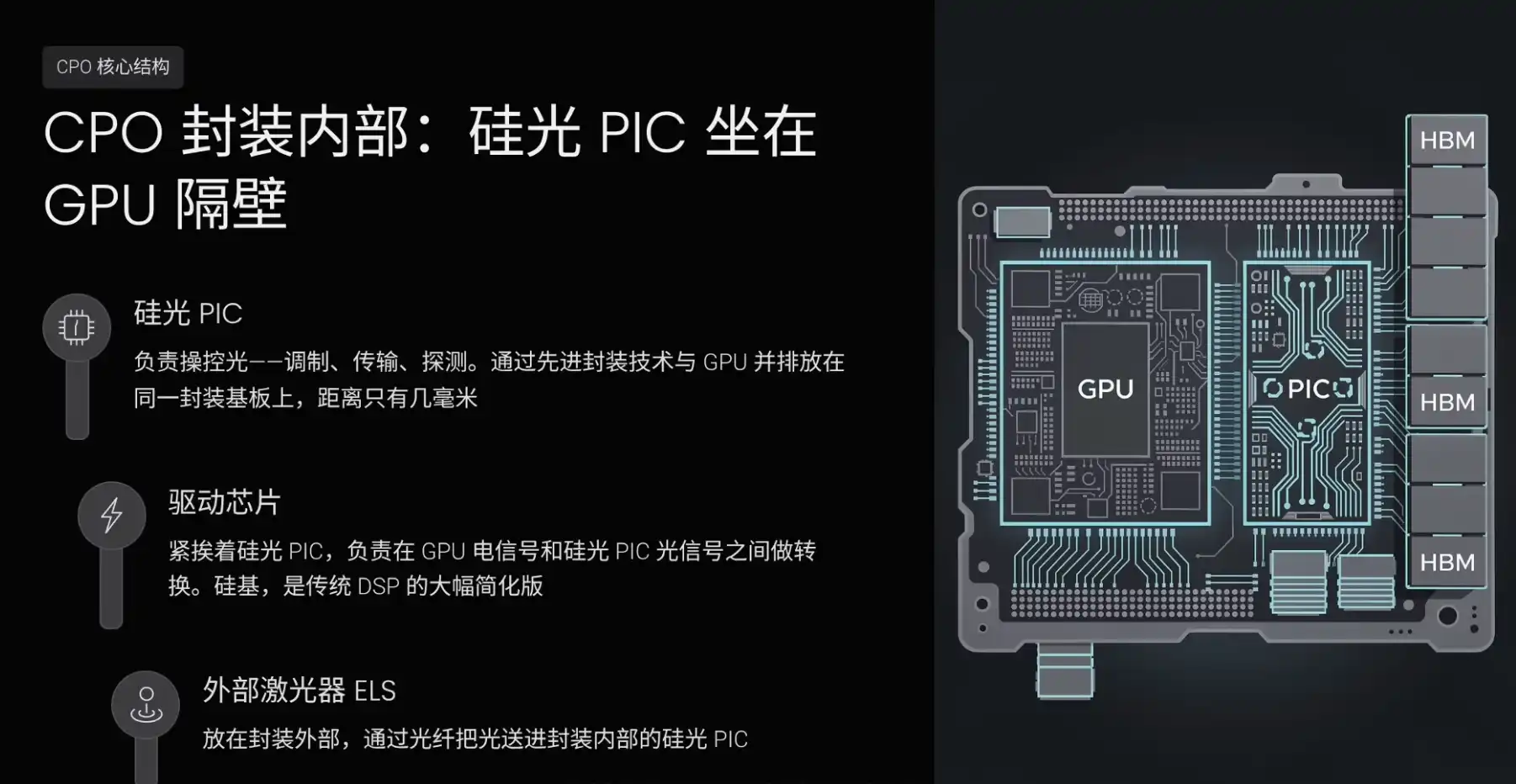
But silicon has a natural flaw: it doesn't emit light. Therefore, silicon photonic PICs can only manipulate light, not generate it. The light source still needs to be provided by an InP laser. This forms the core structure of CPO: a silicon photonic PIC is placed inside the package, responsible for modulating, transmitting, detecting—manipulating light. It is placed side-by-side with the GPU on the same package substrate via advanced packaging technology, only a few millimeters apart, similar to HBM memory sitting next to the GPU.
Next to the silicon photonic PIC, there will also be a driver chip responsible for converting between the GPU's electrical signals and the silicon photonic PIC's optical signals. This is also a silicon-based chip, essentially a significantly simplified version of the traditional optical module's DSP. Because the electro-optical conversion distance in CPO is only a few millimeters, it doesn't need the complex error correction and encoding of a DSP; a simple driver is sufficient.
Outside the package, a laser is placed as an external light source, called an ELS (External Laser Source). The laser sends light into the silicon photonic PIC inside the package via an optical fiber. The laser isn't placed directly inside the package because InP lasers generate significant heat; cramming them together with the GPU and silicon photonic PIC would cause problems. Additionally, laser lifespan is limited; if integrated inside the package and it fails, the entire chip worth tens of thousands of dollars would be scrapped. Making the laser externally pluggable allows for easy replacement without affecting the chip itself.
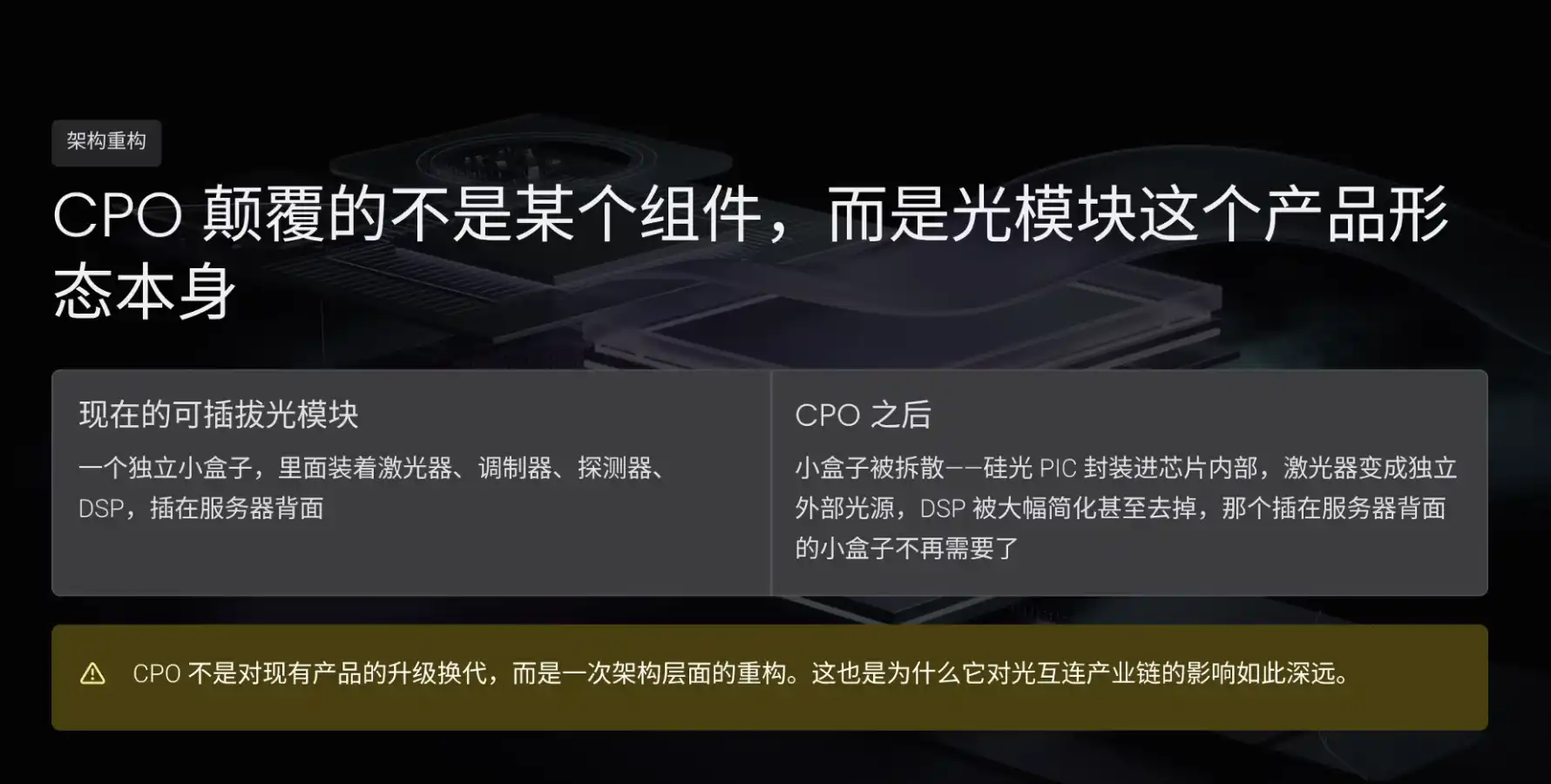
What CPO truly disrupts is not a specific component within the optical module, but the very product form of the optical module. Currently, a pluggable optical module is an independent little box containing the laser, modulator, detector, and DSP. CPO essentially dismantles this box: the silicon photonic PIC is packaged directly inside the chip, the laser becomes an independent external source, the DSP is greatly simplified or eliminated, and the little box on the server's back is no longer needed. This isn't an upgrade to an existing product; it's an architectural-level reconstruction.
Why CPO Became an Investment Theme in 2026
The concept of CPO has existed for many years. Why did it suddenly become a hot investment theme in 2026? Goldman Sachs released a report stating that the potential market size for optical interconnect could expand from the current ~$15 billion to $154 billion by 2028, a roughly 9x growth, with CPO accounting for $91 billion. The core reason is one: NVIDIA's next-generation architecture turned CPO from an option into a necessity.
In the current GB300 NVL72 system, 72 GPUs form one cabinet, with connections between GPUs inside the cabinet still using copper cables. But as AI cluster scale expands to hundreds or even thousands of GPUs, the network connections *between cabinets* become the bottleneck. In its next-generation Rubin platform (NVIDIA's subsequent AI platform code name), NVIDIA introduced a CPO solution for the network switches connecting cabinets, replacing traditional pluggable optical modules. This is the first time NVIDIA officially adopted CPO in its platform.
Moving to the generation after next, Feynman (NVIDIA's further-out AI platform code name), CPO might even enter the GPU interconnect *within cabinets*. In other words, optics are moving step-by-step from between cabinets closer to between GPUs. Lumentum's CEO also confirmed in the latest earnings call that CPO will see massive supply-demand imbalance, with demand far exceeding supply; CPO is Lumentum's single largest growth driver and remains in a very early stage.
Looking at industry data, the current actual shipment volume for CPO is still very small, around $160 million in 2026, mainly consisting of samples and small batches. But if Goldman Sachs' prediction materializes, it could balloon to $91 billion by 2028—a curve from zero to one hundred billion dollars of explosive growth. NVIDIA has already begun mass production of CPO switches in early 2026. Broadcom delivered CPO-related products to customers in October 2025. TSMC launched its COUPE (Chip on Upper Package Edge? Context suggests TSMC's CPO advanced packaging solution) packaging solution. Both NVIDIA and Broadcom adopting CPO indicates it's no longer a distant concept but is becoming a reality.
However, CPO won't completely replace pluggable optical modules in the short term. CPO primarily addresses ultra-high-density AI cluster internal connection needs, such as GPU interconnects within NVIDIA super nodes. Data centers still have many other connection scenarios, including cabinet-to-switch, switch-to-switch, and data center-to-data center, which will likely continue using pluggable optical modules for the foreseeable future. Therefore, a more accurate relationship is that CPO opens up a new market potentially much larger than the pluggable optical module market, rather than simply replacing the existing market. The two will coexist in different scenarios.
The Five Beneficiaries After a CPO Explosion
If CPO truly explodes in the future, even entering a super-cycle, the most beneficial industry chain links roughly fall into five categories.
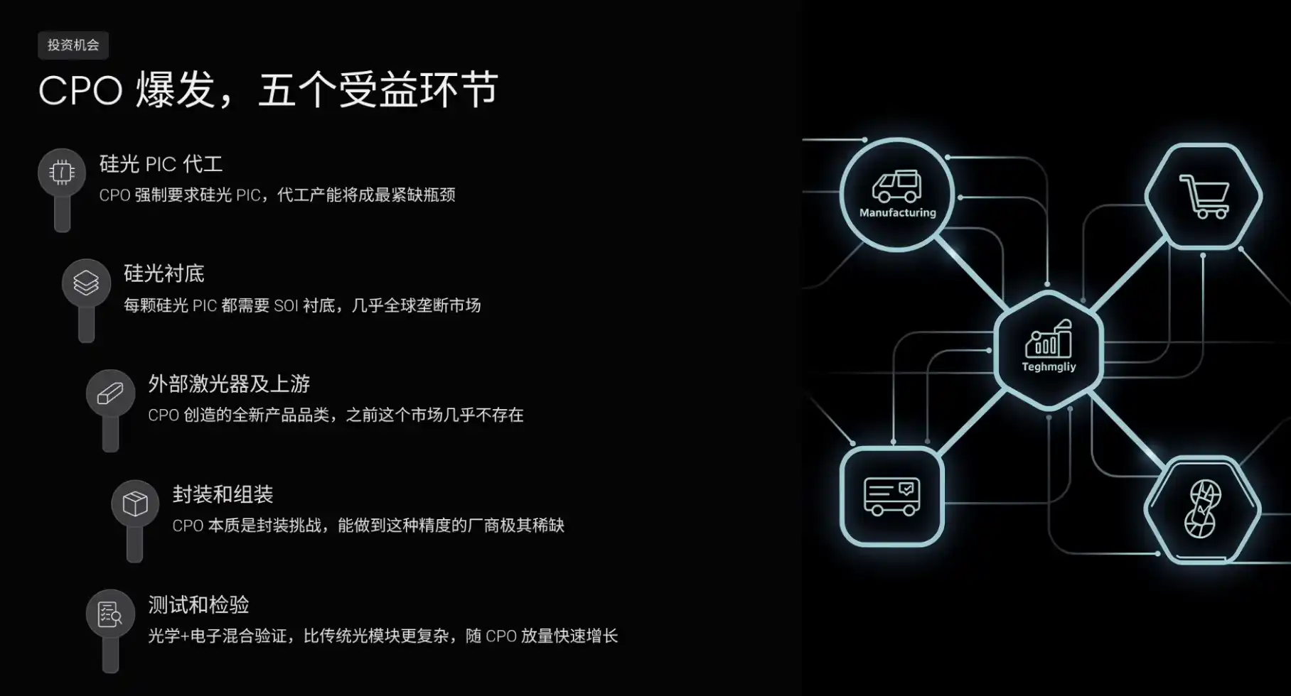
The first is Silicon Photonic PIC foundries. The CPO architecture mandates the use of silicon photonic PICs because only silicon-based chips can be co-packaged with GPUs using advanced packaging. The number of companies capable of silicon photonic PIC foundry services is very limited, making capacity one of the most constrained bottlenecks.
The second is Silicon Photonic substrates. Every silicon photonic PIC requires an SOI substrate. A surge in demand for silicon photonic PICs driven by CPO will also surge demand for SOI substrates, and the SOI substrate market is almost a global monopoly.
The third is External Laser Sources and their upstream supply chain. CPO creates a new product category: traditional pluggable optical modules integrate the laser inside the box, while in the CPO architecture, the laser must be externalized, made into a separate light source. This market barely existed before.
There's also a key process mismatch here. Large laser manufacturers' existing capacity is mainly geared towards producing traditional EML lasers, which integrate light emission and modulation on a single chip for pluggable optical modules, with order contracts booked through 2027-2028. But CPO requires simpler lasers that only emit light, not modulate it, because modulation is handled by the silicon photonic PIC inside the package. While both types use InP, they have different designs and production lines, making seamless switching impossible. Major players' capacity is locked in by traditional laser contracts. Even Lumentum itself has to purchase CPO lasers from the open market, causing spillover demand to flow to independent laser suppliers.
Surging laser demand will further propagate upstream. More lasers mean more InP substrates and more epitaxial wafers. Goldman's report warns that InP substrate supply tightness may persist until 2027.
The fourth is Packaging and Assembly. CPO is essentially a packaging challenge, requiring precise integration of silicon photonic PICs and electronic chips with extremely high accuracy requirements. Companies capable of CPO-level packaging and assembly will be scarce in the future.
The fifth is Testing and Inspection. Every silicon photonic PIC needs optical performance testing and reliability verification before leaving the factory. CPO testing is more complex than for traditional optical modules because it involves mixed optical and electronic verification. This segment will also grow rapidly as CPO volumes increase.
In summary, after a CPO demand explosion, the biggest beneficiaries will be the bottleneck links: silicon photonic foundries, silicon photonic substrates, external laser sources, InP substrates and epitaxy, packaging/assembly, and testing/inspection.
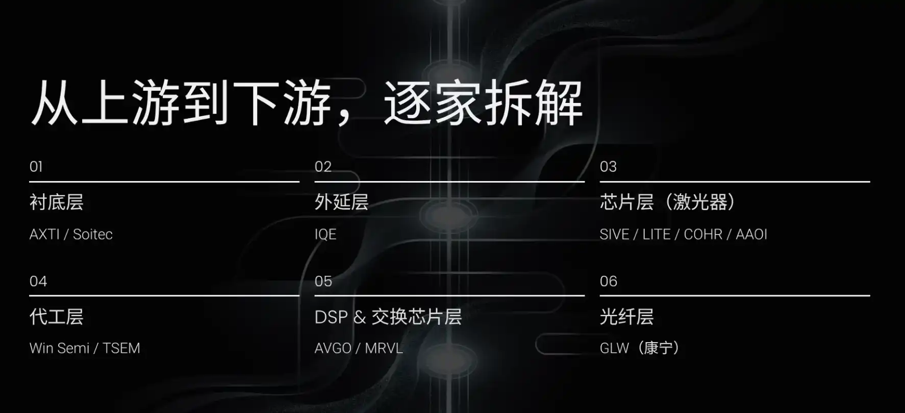
Upstream Substrates: AXTI & Soitec
Looking from upstream to downstream, the two most important companies at the substrate layer are AXTI and Soitec. The two serve different technology paths; they are not competitors but complementary. AXTI serves the laser industry chain, responsible for emitting light. Soitec serves the silicon photonics industry chain, responsible for manipulating light. Optical interconnect requires both.
AXTI is a US company making InP and GaAs substrates. Its job is to purify rare elements like Indium, Phosphorus, Gallium, Arsenic, synthesize them, pull them into single-crystal ingots, and slice them into thin wafers. AXTI's irreplaceability lies in the fact that there are very few companies globally capable of making high-quality InP substrates, aside from AXTI, only a few like Japan's Sumitomo Electric and Germany's Freiberger. AXTI's moat is its accumulated expertise in material purity processes, decades of know-how, and long customer qualification cycles. Downstream customers switching suppliers would require re-qualifying the entire product line, making the switching cost high.
CPO won't bypass InP substrates; it will amplify demand for them. In the CPO architecture, each GPU needs an external laser; the number of lasers directly correlates with the number of GPUs. More lasers mean more InP substrates. Therefore, CPO is a clear positive for AXTI. AXTI's investment profile is small-cap, high-beta, with lagged demand transmission, but once orders materialize, stock price elasticity could be significant.
Soitec is a company listed in Paris, France, making SOI silicon photonic substrates. Soitec holds a dominant market position in the niche of SOI substrates dedicated to silicon photonics and invented the patented Smart Cut technology. The core of CPO is silicon photonic PICs, and every silicon photonic PIC requires an SOI substrate, making Soitec a likely strong beneficiary in a CPO super-cycle. Its valuation was around 1.4x book value, relatively low for a global monopolist. Note: Soitec is listed on the Paris exchange, not in the US.
Epitaxy Layer: IQE/IQEE
Moving downstream is the epitaxy layer. The world's significant independent epitaxy supplier is IQE/IQEE, listed in London. IQE's moat lies in the high difficulty of epitaxy itself. Epitaxy involves growing functional layers like a mille-feuille on the substrate, each layer only a few nanometers thick. Any minor deviation in material, temperature, or growth time can render a laser unusable. These parameter combinations constitute the epitaxy recipe, which IQE has accumulated over decades; it's not something that can be replicated quickly with capital.
After a CPO explosion, IQE's logic is similar to AXTI's: CPO amplifies laser demand; more lasers need more epitaxial wafers. IQE's risk lies in high customer concentration, with LITE being a major client. If LITE decides to do its own epitaxy in the future, pushing vertical integration, IQE's largest revenue source could be impacted—a single-point risk to note before investing.
Laser Layer: SIVE/SIVEE, LITE, COHR, AAOI
Continuing downstream into the chip layer, the most scarce link here is the laser. Core companies include SIVE/SIVEE, LITE, COHR, and AAOI.
SIVE/SIVEE is one of the most explosive performers among optical interconnect stocks over the past year. It's a small Swedish-listed company with a market cap around $1.5 billion and annual revenue about $30 million. It leans towards a Fabless model, possessing its own InP100 platform and a small fab in Glasgow, UK, giving it some manufacturing capability. It also partners with Taiwan's Win Semi, outsourcing laser design to mature foundry capacity to scale high-power laser production.
SIVE/SIVEE has five core strengths. First, its InP100 standardized platform modularizes the laser's core, allowing rapid assembly of different specification products like building blocks. Second, wafer-level testing, testing each die directly on the wafer before dicing, improving yield and reducing cost. Third, covering both current and next-generation technologies, with products for both pluggable optical module lasers and CPO external light sources. Fourth, parallel operation across multiple tracks besides AI data center optical interconnect, such as LiDAR, satellite communications, and defense, diversifying single-market risk. Fifth, a light-asset expansion model: small fabs handle core verification and small batches, while large-scale production leverages Win Semi's capacity, avoiding heavy capital expenditure on building massive fabs while retaining core manufacturing knowledge.
SIVE/SIVEE is a high-beta play in a CPO super-cycle. One reason is that major players' capacity is locked by traditional laser orders, so spillover demand for CPO external light sources needs to be absorbed by independent laser suppliers. Another reason is that it's already embedded in the supply chains of several CPO projects. AMD's CPO solution is being pushed through the GlobalFoundries platform, with SIVE being one of the few laser suppliers within that ecosystem; Marvell's Celestial AI and Ayar Labs are also among its customers.
However, SIVE/SIVEE's risks are also evident: revenue is very low, and most customers are still in development and verification stages, not yet in formal mass production. If even just two or three customers materialize, the stock price could continue rising; if customers delay or cancel, the stock could see significant pullbacks. Think of it as a high-payoff lottery ticket.
LITE, or Lumentum, represents the IDM route for lasers. It handles both laser design and manufacturing, plus complete optical module assembly. LITE's core highlight is NVIDIA's $2 billion strategic investment and multi-billion dollar procurement commitment, directly locking up its capacity. Additionally, LITE is deeply embedded with Google's TPU ecosystem; Google's AI data centers heavily use LITE's optical switching technology and lasers.
LITE's CEO made three key statements on the earnings call: CPO will see large-scale supply-demand imbalance; CPO is Lumentum's single largest growth driver; CPO is still in a very early stage. This is essentially the industry's frontline CEO personally confirming a CPO super-cycle. LITE's capacity is booked through 2028. Its moat is the dual major-customer lock with NVIDIA and Google. The risk is that capacity being locked by NVIDIA also means its near-term ceiling is set; revenue primarily depends on NVIDIA's orders, giving the company limited autonomy, so its growth curve isn't as steep as SIVE/SIVEE's potential.
COHR, or Coherent, is a rare vertically-integrated company covering the entire stack in the optical interconnect space. It can handle everything from materials, InP lasers, silicon photonic PICs, to optical modules. Its optical module market share is in the global top tier, around 20%. Like LITE, COHR also received a $2 billion strategic investment and multi-billion dollar procurement commitment from NVIDIA.
COHR's advantage is that no matter which direction the technology evolves, it's less likely to miss out. CPO needs silicon photonic PICs—it can do that. CPO needs lasers—it can do that. Pluggable optical modules continue to exist—it can do that too. That's the value of full-stack coverage. COHR is more like a mid-cap, relatively safe optical interconnect play, with high certainty, less upside than SIVE/SIVEE, but lower volatility and risk.
AAOI is one of the few vertically-integrated optical interconnect companies based in the US. It uses MBE (Molecular Beam Epitaxy) equipment to grow epitaxial layers on InP substrates, manufactures its own laser chips, packages optical sub-assemblies, and assembles finished optical modules. Its current core business is 800G and 1.6T pluggable optical modules. The transcript states that AAOI secured its first large-volume order for 1.6T data center optical modules in March, with an initial order exceeding $200 million, followed by a $71 million 800G order in April.
AAOI won't necessarily be disrupted by CPO. First, pluggable optical modules won't disappear because of CPO's rise; CPO addresses connections inside super nodes, but many connections between cabinets will still require pluggable modules. Second, AAOI is entering the CPO supply chain. In the CPO architecture, the laser cannot be placed inside the package; it must be externalized into a small module that sends light in via fiber. AAOI's showcased new product is precisely an external laser source dedicated to supplying light for CPO. Overall, AAOI's strengths are vertical integration, the supply chain security narrative of US-based manufacturing, and the extension potential of its laser technology into CPO external light sources. But it's also a small-cap, high-beta stock—high volatility, high potential upside, but also high risk.
Foundries: Win Semi & TSEM
After lasers, let's look at foundries. The two most critical companies are Win Semi and TSEM.
Win Semi is one of the world's largest pure-play compound semiconductor foundries, offering both GaAs and InP foundry services. SIVE/SIVEE's laser mass production is primarily handled by Win Semi. The next-generation CPO architecture amplifies demand for external lasers, and Win Semi is the most important foundry partner for these laser design companies. Regardless of which laser design company ultimately wins, they will likely need Win Semi for manufacturing.
TSEM is the Israeli specialty foundry, called by the market the "TSMC of optical interconnects." It could be one of the most direct beneficiaries in a CPO super-cycle. The core of CPO is silicon photonic PICs, and TSEM is the foundry with the highest market share in silicon photonic PICs. CPO mandating silicon photonic PICs essentially pushes TSEM's silicon photonics foundry business from a niche to the center of the industry chain.
Most of TSEM's capacity is already booked through 2028. Even so, its forward P/E is only around 16-18x, leaving room for upside given high CPO growth expectations. Core risk is geopolitics; it's an Israeli company located in the Middle East, potentially affected by regional conflicts.
Both Win Semi and TSEM are foundries, but the core difference is the material used and the objects manufactured. Win Semi uses InP and GaAs to make lasers, responsible for emitting light. TSEM uses SOI substrates to manufacture silicon photonic PICs, responsible for manipulating light. The two material systems are incompatible; they are not competitors but foundries serving different links in the industry chain.
DSP & Switch Chip Layer: Broadcom & Marvell
Moving further downstream is the DSP and switch chip layer, primarily Broadcom and Marvell.
Broadcom AVGO is a trillion-dollar US stock giant with businesses including switch chips, custom AI accelerator chips, enterprise software, etc. Two segments directly related to optical interconnect: First, DSP chips, the brain of the optical module responsible for error correction/encoding; Broadcom is one of the most important suppliers in this field. Second, CPO switches; Broadcom's third-generation CPO switches have entered mass production—these are new switches with optical engines packaged directly beside the switch chip. In terms of CPO commercialization progress, Broadcom is arguably ahead of even NVIDIA.
But from an investment perspective, optical interconnect is just one of Broadcom's many businesses, not a large portion of its overall revenue. Its stock price won't multiply several times just because CPO explodes. Investing in Broadcom means buying the comprehensive certainty of AI infrastructure, not the single-point upside of the optical interconnect industry explosion.
MRVL, or Marvell Technology, is also a diversified chip company involved in custom AI accelerator chips, data center networking chips, storage chips, etc. Two segments directly related to optical interconnect: First, DSP chips—Marvell and Broadcom are the two core suppliers in this field, competing head-on. Second, CPO. Marvell's acquisition of Celestial AI significantly enhanced its capabilities in silicon photonic interconnect.
The core logic of this episode is that GPUs originally used copper cables for communication, now being replaced by optics. What Celestial AI does is also in this direction, just at a shorter distance: replacing copper with light *inside* the chip package. Through this acquisition, Marvell's strategic position in the CPO direction is significantly strengthened.
Compared to Broadcom, Marvell's exposure to optical interconnect is more concentrated. Broadcom is a trillion-dollar company where optical interconnect is just one part; Marvell is smaller, with revenue of $8.2 billion last fiscal year, up 42% YoY, with management projecting near $15 billion over the next two fiscal years. Optical interconnect and CPO likely account for a larger portion of Marvell's overall revenue, offering more potential upside. Marvell isn't a pure-play optical interconnect stock, but could be a good choice with combined exposure to both DSP and CPO directions.
Underlying Fiber: Corning
Finally, the foundational company GLW, Corning. Corning is a global leader in optical fiber. Many know Corning from Apple iPhone screen glass, but in reality, optical communications is already one of Corning's largest and fastest-growing divisions. Since inventing communication fiber in 1970, Corning has laid millions of miles of optical cable.
Regardless of which optical module company wins, regardless of whether the technology path is pluggable or CPO, Corning's fiber is needed. In the CPO architecture, fibers still connect the external laser to the silicon photonic PIC, and connections between different cabinets continue to use fibers. Fiber is one of the few links in the entire industry chain unaffected by technology path disputes.
Corning's recent customer bindings are strong. In January this year, Meta announced investing up to $6 billion to help Corning expand its optical cable factories. NVIDIA also announced a multi-year cooperation agreement with Corning, investing $500 million for warrants in Corning. Corning committed to increasing its US optical connectivity capacity tenfold, fiber production by over 50%, and building three new factories.
Previously, NVIDIA invested $2 billion each in LITE and COHR; now it's investing $500 million in Corning. You can see NVIDIA systematically extending the AI infrastructure competition from chips to fiber, locking down the entire optical interconnect supply chain. Corning is one of the relatively highest-certainty, lowest-upside plays in the entire optical interconnect industry chain.
Three Allocation Approaches: Conservative, Balanced, Aggressive
After discussing so many companies, we need to answer "how to invest." The most important rule is: the further upstream you go, the smaller the companies, the greater the potential upside, but the lower the certainty; the further downstream you go, the larger the companies, the higher the certainty, but the smaller the upside. The most upstream substrate and epitaxy companies, like AXTI, IQE, have small market caps, lagged demand transmission, but once demand materializes, upside can be significant. Downstream giants like AVGO have high certainty but can't be expected to quintuple in a year.
The first approach is Conservative allocation, with core holdings being AVGO, MRVL, and GLW. All three are relatively large-cap companies: Broadcom is around $2 trillion market cap, in the top 10 US stocks; Marvell and Corning are near the $100 billion range. Broadcom and Marvell are diversified, with optical interconnect just one part; Corning, though more focused, provides fiber, a necessity unaffected by technology path disputes. This portfolio's characteristic is limited downside risk; even if optical interconnect development falls short, other businesses can support the stock price, suitable for long-term investors unwilling to take on too much volatility.
The second approach is Balanced allocation, with core holdings being COHR, LITE, and TSEM. These three are leaders in their respective segments, medium-sized, offering both certainty and upside potential. COHR is the full-stack optical company, less likely to miss out regardless of industry direction, with NVIDIA's $2 billion investment providing a safety net. LITE is the laser core supplier with locked capacity by NVIDIA, its CEO personally confirmed CPO imbalance. TSEM is the foundry with the highest share in silicon photonic PICs, relatively inexpensive valuation. If you want exposure to optical interconnect and can tolerate some volatility, this portfolio is relatively suitable.
The third approach is Aggressive allocation, with core holdings being SIVE/SIVEE, AAOI, SOI/Soitec, AXTI, IQE. All five are in upstream bottleneck links. SIVE/SIVEE is a scarce supplier of CPO external light source lasers, embedded in multiple CPO project supply chains. AAOI is a high-beta play on pluggable optical modules, with capability to enter CPO external light sources. Soitec is the overwhelmingly dominant supplier in silicon photonic substrates. AXTI provides InP substrates needed for laser manufacturing. IQE handles the critical epitaxy for laser manufacturing. If the CPO super-cycle unfolds at the pace predicted by Goldman, this portfolio offers the greatest upside but also carries the highest risk.
These small-cap stocks can easily drop 20%-30% in a single day; it's best to keep positions within 5%-10% of your total portfolio. Also note, many small-cap optical interconnect stocks are not listed in the US. Soitec is on the Paris exchange, IQE in London, SIVE in Sweden, Win Semi in Taiwan. Using a broker like Interactive Brokers, most are tradable, but you need to enable permissions for those markets.
Sector Risks: CPO Timeline, NVIDIA's Choices, Small-Cap Volatility
The entire sector also has clear investment risks.
First, uncertainty in CPO commercialization timeline. Goldman's prediction of a $91 billion CPO market is quite aggressive. Achieving this number requires NVIDIA's next-generation architecture to launch on schedule, CPO yields to meet targets, InP substrate supply to keep up, cloud providers' capital expenditures to remain high, and continuous capital flowing into the industry chain. Any link faltering would reduce the actual figure.
Second, NVIDIA's choices are crucial. What optical interconnect solutions NVIDIA's next-generation Rubin platform adopts will directly impact the entire supply chain landscape. Currently, NVIDIA has included CPO in the Rubin reference architecture, but specific supplier choices and mass production timing remain uncertain.
Third, inherent risks of small-cap stocks. Many companies in the optical interconnect chain have very small market caps. Such stocks shouldn't be heavily weighted, and certainly not leveraged.
Three Core Judgments & Conclusion
Finally, summarizing my three judgments on the optical interconnect sector.
First, optical interconnect is not hype. The interconnect demand in AI data centers is real, urgent, and irreversible. The more GPUs sold, the greater the optical interconnect demand. This is a certain track strongly tied to the GPU industry chain.
Second, CPO is the biggest future increment in this track. Goldman predicts the optical interconnect market could grow 9x, with CPO accounting for $91 billion; Lumentum's CEO personally confirmed severe CPO supply-demand imbalance, still in early stages; NVIDIA has written CPO into its next-generation architecture, indicating it's not a distant story but happening now.
Third, if you can tolerate high risk and high volatility, seeking high returns, the core logic is to target bottlenecks. The optical interconnect industry chain isn't like GPUs, dominated by one player; it has extremely fine division of labor and highly scattered bottlenecks. Behind each bottleneck link, often only one or two companies can do it. Finding these bottlenecks means finding the greatest Alpha in this track.
To conclude with one more line: GPUs are the brain of AI, but the neural network *between* these brains is what determines how fast the entire system can run. Optical interconnect is the neural network of AI. Without it, more GPUs are just isolated islands. This industry chain, obscured by GPU's glare, potentially reaching trillions in the future, might be brewing the next very significant investment opportunity.
Of course, volatility and risk in the optical interconnect sector will also be very high. None of the above constitutes investment advice. Before investing, be sure to consider the underlying returns and risks, combined with your actual portfolio positioning and cash flow, before making decisions.