Crossing the 'Memory Wall': The Wafer-Level Revolution and Computing Power Routes in the AI Inference Era

marsbitPublicado em 2026-06-05Última atualização em 2026-06-05

Resumo

In 2026, a historic shift occurred in AI as major cloud providers' inference spending surpassed training spending for the first time, signaling a move from "building large models" to "using large models." This shifts the core challenge from computing power to the "memory wall"—the bottleneck of data movement (model weights, activations, KV Cache) between external DRAM and processors, where energy and latency from data transfer far exceed computation itself. Companies like Nvidia face GPU idle time due to bandwidth limits. In contrast, Cerebras Systems adopts a radical "wafer-scale" approach with its Wafer-Scale Engine (WSE). Instead of cutting a silicon wafer into many chips, Cerebras uses almost the entire wafer as one massive chip (WSE-3). This design provides 44GB of on-chip SRAM, delivering memory bandwidth thousands of times higher than traditional HBM (e.g., 21 PB/s vs. Nvidia B200). For LLM inference, weights are streamed layer-by-layer from external MemoryX storage to the chip, avoiding HBM bottlenecks. This results in token generation speeds 1.5–5 times faster than Nvidia's B200 in some models and significant advantages in first-token latency and long-context tasks. Additionally, Cerebras's architecture offers much lower interconnect power consumption (0.15 pJ/bit vs. GPU's ~10 pJ/bit). However, Cerebras faces challenges: SRAM scaling has slowed with advanced nodes, limiting future capacity gains; the chip requires specialized liquid cooling and custom software sta...

In 2026, the global development of AI reached a landmark inflection point—the capital expenditure on inference by hyperscale cloud vendors historically exceeded that on training for the first time. The industry's anchor shifted from 'training large models' to 'using large models,' fundamentally flipping the structure of computing demand.

In the training era, the core challenge of computing power was 'double-precision floating-point and cluster scale'; entering the inference era, the core challenge became 'memory bandwidth and communication latency.'

The bottleneck for large model inference is no longer merely computation, but data movement—model weights, intermediate activations, and KV Cache need frequent interaction between off-chip DRAM (like HBM) and GPUs. The larger the model, the higher the energy consumption and latency of data transfer, ultimately far exceeding the energy consumption of computation itself, thus forming the memory wall.

NVIDIA GPUs have built a solid fortress with CUDA and NVLink, but still cannot avoid GPU idling caused by bandwidth bottlenecks.

A domestic large model company, Zhipu, conducted a simple experiment: In a 512-card inference cluster, keeping the GPUs, model, and code unchanged, but only upgrading the network bandwidth cap from 200GB/s to 400GB/s, inference throughput directly increased by 10%, and first-token output latency decreased by 19%—the principle is simple: widen the road, and the cars can run faster.

However, non-GPU architectures represented by Cerebras seem to be tearing an opening in this memory wall.
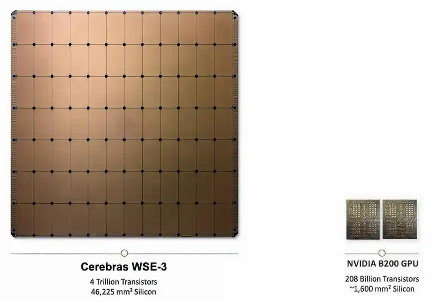
Size comparison between Cerebras WSE-3 chip and NVIDIA B200 GPU

The Essence of Cerebras: A Near-Memory Computer Based on SRAM

Cerebras Systems was founded in Silicon Valley by Andrew Feldman and others. The early founding team all came from SeaMicro, a low-power microserver company that was later acquired by AMD. Subsequently:

In 2015, the founding team established the 'wafer-scale computing' route.

In 2016, they completed registration and Series A financing, entering a stealth R&D phase.

In 2019, they released their first product, the WSE-1 chip and CS-1 system, based on TSMC's 16nm process.

In 2021, they released the second-generation product, based on TSMC's 7nm process.

In 2024, they released the third-generation product (WSE-3 / CS-3), based on TSMC's 5nm process. Both the chip and system are manufactured entirely in the USA, making it a genuinely pure US-made chip system.
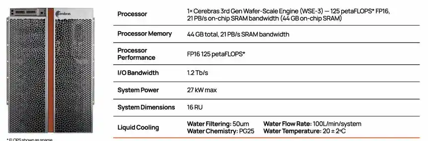
CS-3 system configuration, containing 1 WSE-3 chip

Cerebras's Wafer-Scale Engine (WSE) architecture philosophy is simple, direct, yet hits the pain point: trade extreme physical expansion for extreme compression of data movement latency.

Ordinary chips slice a wafer into many small chips; NVIDIA GPUs follow this approach. Cerebras does the opposite: don't slice, directly turn nearly the entire wafer into one giant chip, called the Wafer-Scale Engine (WSE).

Traditional chips are formed by cutting a 300mm diameter wafer into hundreds of small chips; Cerebras chooses to keep the entire wafer intact, using it directly as the whole chip. The latest WSE-3 boasts 4 trillion transistors, 900,000 AI cores, each equipped with 48KB of local SRAM, giving the entire chip 44GB of on-chip SRAM, providing 21 PB/s of on-chip memory bandwidth and 214 Pb/s of fabric bandwidth—thousands of times the bandwidth of traditional HBM.
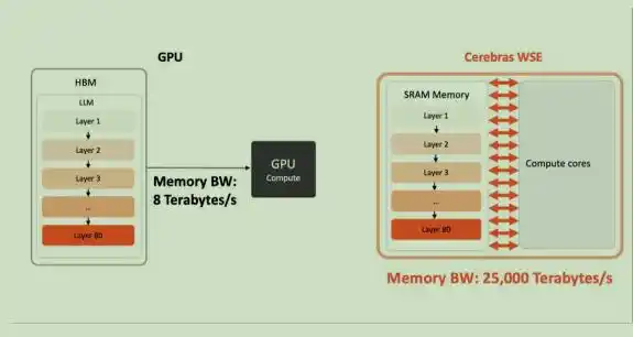
Cerebras WSE's memory bandwidth is 2625 times that of NVIDIA's B200 packaged chip, breaking the memory bandwidth bottleneck in large model inference scenarios.

In Cerebras's architecture, model weights are never stored on the SRAM but reside in off-chip storage (MemoryX) and are transferred layer by layer to the giant chip. The approach involves separating the storage of neural network model weights from the computing units.

All model weights are stored externally in the MemoryX memory extension module. The weights required for computing each layer of the network are transmitted layer by layer to the CS-3 system on demand. Weights are stored in the DRAM and flash memory of MemoryX and transmitted to the CS-3 system at full bandwidth rates. These weights are not stored in the CS-3 system—not even temporarily cached—CS-3 relies on the core's underlying dataflow mechanism to complete computations.

Leveraging its wafer-scale architecture, Cerebras demonstrates barrier-breaking advantages in LLM inference constrained by memory bandwidth. When generating tokens sequentially, weights are streamed layer by layer from off-chip MemoryX to CS-3. For different models, the token rate is 1.5 to 5 times that of NVIDIA's B200.
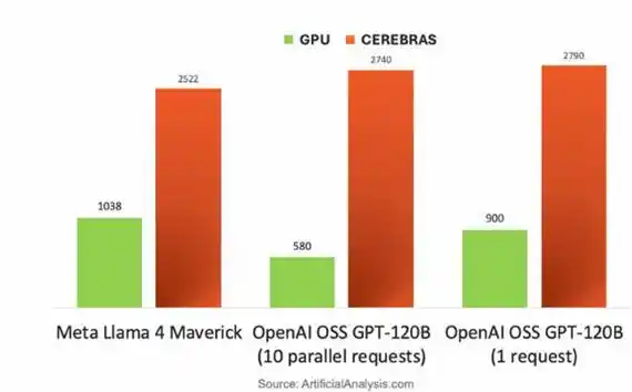
NVIDIA DGX B200 GPU versus Cerebras CS-3 chip, token rate comparison when running different large models

Its core advantage lies in: The 44GB of on-chip SRAM in CS-3 provides 21 PB/s of ultra-high bandwidth (2625 times that of B200) and 214 Pb/s of interconnect bandwidth, freeing weight streaming from HBM interface limitations. Therefore, it performs exceptionally well in TTFT (Time To First Token), long-context, and agent workload scenarios.

Although weights are external to MemoryX, loaded layer by layer on demand, and not cached on-chip, CS-3 relies on the core's dataflow mechanism to perform lossless full FP16 precision computations in SRAM; leveraging linear performance scaling, it also unleashes astonishing total throughput in multi-user concurrent inference.

Besides bandwidth, there is also a power advantage. Recently, in a speech, Sutong Liu, Chairman of InnoLight, mentioned that customers' requirement for optical modules is 1 pJ/bit, while the current level is 10 pJ/bit. In Cerebras chips, the interconnect power consumption is only 0.15 pJ/bit, whereas the current GPU interconnect power consumption is 10 pJ/bit.
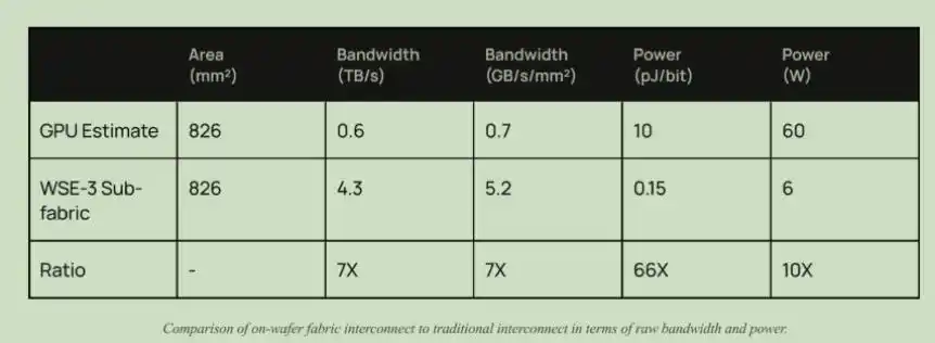
Bandwidth and power consumption comparison between Cerebras interconnect and GPU interconnect architectures

Thus, if Cerebras's wafer-scale large-chip architecture becomes mainstream for AI inference or even training, it might significantly suppress and structurally alter the shipment volumes of traditional optical modules and CPO (Co-Packaged Optics). The core logic is: the high demand for optical modules and CPO essentially aims to solve the bandwidth bottleneck of 'chip-to-chip interconnect' and 'node-to-node interconnect' in GPU clusters; Cerebras's architecture precisely solves the problem by 'eliminating distributed interconnects.'

Counterintuitive: The 'True and False' Fatal Flaws of Wafer-Scale Large Chips

The core of chips always lies in Trade-Off. To achieve extreme on-chip SRAM bandwidth, Cerebras also brings some issues.

Low Yield?

Quite the opposite. The size of a single AI core is reduced to 0.05 square millimeters (1% the size of a single H100 compute core), resulting in higher yield. By routing on-chip, defective cores can be disabled and bypassed, improving defect tolerance by 100 times compared to traditional multi-core processors. The chip actually has 1 million AI cores, but considering yield, it is advertised as having 900,000 AI cores.

Only Good at Inference, Not at Training?

In the years following Cerebras's founding, training was the mainstream topic, so the company focused heavily on training. It's only after inference demand surged that people realized its advantages in inference were more pronounced.

In reality, simplified distributed computing also brings advantages like reduced code complexity and lower communication overhead.

Training a 175-billion-parameter model on 4000 GPUs typically requires about 20,000 lines of distributed training code.

Cerebras achieves equivalent training with 565 lines of code—the entire model can be placed on the wafer without dealing with data parallelism complexity.

SRAM Scaling is Dead; Core Advantage Faces a Physical Ceiling.

The third-generation product is based on TSMC's 5nm, and its SRAM capacity only increased by 10% compared to the second-generation product based on TSMC's 7nm. Beyond 5nm, SRAM cell area hardly shrinks with process node advancement.

This means Cerebras can no longer significantly increase its core advantage (SRAM capacity) by upgrading TSMC's process nodes (e.g., from 5nm to 3nm) as it did before.

Limited by wafer size, cooling capability, and manufacturing costs, on-chip storage resources like SRAM are difficult to scale linearly with computing cores, encountering a resource ratio bottleneck. This almost blocks its evolutionary path.
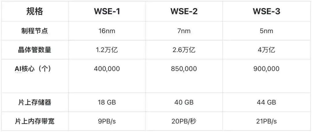
Technical specifications of Cerebras's three product generations

The Triple Purgatory: Cooling, Process, and Ecosystem.

The entire wafer concentrates heat, leading to high heat flux density, necessitating reliance on customized data centers and dedicated liquid cooling systems. Moreover, ecosystem compatibility means customers must adapt to its customized software stack, with weak compatibility with existing general-purpose programming frameworks like CUDA, leading to high software porting and adaptation costs.

Low Off-Chip Bandwidth Creates an Expansion 'Island'.

Due to the limitations of wafer-scale physical design, the number of I/O pins that can be led out from the edge of the WSE is extremely limited, resulting in an I/O bandwidth of only 150GB/s. Compared to NVIDIA NVLink's 1.8TB/s bi-directional bandwidth, it's like a snail. This makes it extremely difficult for WSE to scale out at high speeds. Although Cerebras's SwarmX interconnect performs decently in multi-system combinations, in the face of super-large models requiring high-speed multi-chip interconnection, the extremely low off-chip bandwidth becomes a structural physical shackle.

Route Competition: Big Tech In-House Development—How Much Window Does Cerebras Have Left?

Big tech companies have multiple parallel paths to address 'inference requiring higher bandwidth + lower latency,' not just wafer-scale. They are encircling and suppressing the technological dividends of startups like Cerebras through three concurrent approaches.

1 In-House ASIC Development

Google TPU v8 has already split into training-specific and inference-specific versions; AWS Trainium 4 is on the way; Microsoft Maia is already in use within Azure, built on TSMC's 3nm process, with native FP8/FP4 tensor cores, a redesigned memory system equipped with 216GB HBM3e, and 272MB on-chip SRAM; even Anthropic has begun evaluating in-house inference chip development.

This path is highly probable and will directly cause the TAM (Total Addressable Market) for 'third-party inference procurement' in 2028 to be compressed by 10% to 25%.

2 Process Generalization of the Standard Packaging Route

This is the most direct dimensional reduction attack on Cerebras.

TSMC's SoW (System-on-Wafer) is already widely open to customers, and CoWoS 9.5x interposer will launch in 2027.

What these two products do—stitching multiple dies at the wafer level—essentially makes Cerebras's physical process generic and accessible to all.

NVIDIA's Vera Rubin will enter this ecosystem in the second half of 2026.

Although Cerebras's own cross-reticle stitching is exclusive, the exclusivity window lasts at most 2 to 3 years. Beyond 2027-2028, its process barrier will be diluted by TSMC's advanced packaging.

3 Breakthrough of Optical Interconnect/Optical Computing

The interconnect and memory wall of electronic chips have reached their limits. Photonics' high bandwidth, low latency, and zero crosstalk are the ultimate solution.

Optical routes represented by Lumentum are rising. The biggest advantage of wafer-scale is on-chip computing, but models will inevitably grow larger, making high-speed interconnect beyond wafer scale a necessity.

With the maturity of CPO (Co-Packaged Optics) and Optical Interconnects, it's highly likely we will see optical I/O directly introduced into WSE wafers, breaking the shackles of electrical interconnect. NVIDIA might also acquire companies with specific architectural advantages like LPU (e.g., Groq), combine them with optical interconnects, and develop wafer-scale systems compatible with existing NV super-node software.

Sprinting on the Cliff: Cerebras's Business and Delivery

Cerebras is currently facing a cliff-edge sprint forced by massive orders.

Deals with leading clients like OpenAI are forcing Cerebras to transform from a chip company into a new type of cloud service provider. It no longer just sells hardware but needs to lock in and build massive data center power and facilities in the short term.

According to contract requirements, Cerebras needs to deliver 250MW of data center capacity annually from 2026 to 2028. However, wafer-scale systems have extremely high requirements for data center rooms and cannot be directly placed into traditional air-cooled IDCs. Currently, Cerebras's progress in preparing data center capacity is significantly behind the contract requirements.

From tape-out to factory construction, from power approval to cooling system deployment—this is a quagmire of heavy assets and long cycles.

Epilogue: Left or Right?

Returning to the initial proposition, as the inflection point for inference computing power has arrived, the core of computing architecture always lies in trade-offs.

There is no absolute right or wrong, only the relatively optimal solution for the most important workloads. And workloads are already changing.

Cerebras goes left, choosing extreme physical optimization, trading the entire wafer and massive SRAM for extreme low latency for a single task, which is unbeatable in scenarios extremely sensitive to first-token latency.

NVIDIA goes right, choosing to maintain generality, using HBM + NVLink + massive cluster throughput to handle ever-changing workloads, responding with constancy to change.

The winds are shifting, and the road ahead is uncertain. It is precisely this dual uncertainty of technology and business that breeds the possibility of disruption. In the torrent of computing power flowing towards AGI, it is still too early to draw conclusions—because of uncertainty, there is opportunity.

This article is from the WeChat public account "Garlic Particle Machine Research Institute," author: Pili Youxia (Thunderbolt Ranger)

Criptomoedas em alta

Perguntas relacionadas

QWhat is the key structural shift in the global AI industry in 2026, as identified in the article, and what does it signify?

AIn 2026, the global AI industry reached a pivotal inflection point where for the first time, capital expenditure on inference by hyperscale cloud providers surpassed that on training. This marks a fundamental shift in the focus of the industry from 'forging large models' to 'using large models', fundamentally flipping the structure of computing demand.

QWhat is the 'memory wall' in the context of large model inference, and how does Cerebras' WSE-3 architecture attempt to overcome it?

AIn large model inference, the 'memory wall' refers to the bottleneck caused by the energy consumption and latency of frequently moving data (model weights, intermediate activations, KV Cache) between off-chip DRAM (like HBM) and the GPU, which eventually far exceeds the energy cost of computation itself. Cerebras' WSE-3 architecture attacks this by using an entire wafer as a single, massive chip, packing 44GB of on-chip SRAM. This provides 21 PB/s of on-chip memory bandwidth, which is 2625 times the bandwidth of Nvidia's B200 GPU, drastically reducing data movement latency and breaking the memory bandwidth bottleneck for inference.

QAccording to the article, what are the three main parallel paths that major tech companies are taking to compete with specialized solutions like Cerebras?

AMajor tech companies are pursuing three parallel paths to address the need for higher bandwidth and lower latency in inference, thereby challenging specialized players: 1) Developing their own ASIC chips (e.g., Google TPU v8, AWS Trainium 4, Microsoft Maia). 2) Adopting standardized packaging processes like TSMC's SoW (System-on-Wafer) and CoWoS, which essentially democratize wafer-scale integration techniques. 3) Exploring breakthroughs in optical interconnects/computing (e.g., CPO, Optical Interconnects) to overcome the limits of electrical interconnects.

QWhat are the main potential weaknesses or challenges of the Cerebras wafer-scale chip (WSE) architecture, as outlined in the article?

AThe article highlights several challenges for Cerebras' wafer-scale architecture: 1) A physical scaling limit for SRAM, as SRAM cell area barely shrinks with process nodes beyond 5nm, blocking a key path for increasing its core advantage. 2) Significant thermal management challenges requiring specialized liquid-cooled data centers. 3) A weak software ecosystem and compatibility with existing frameworks like CUDA, leading to high adaptation costs. 4) Very low off-chip I/O bandwidth (150GB/s) compared to alternatives like NVLink, making the system a potential 'island' and hindering high-speed scaling for very large models.

QWhat critical business challenge is Cerebras currently facing due to large customer contracts, according to the article?

AFacing massive orders from leading customers like OpenAI, Cerebras is being forced into a 'cliff-side sprint' to transition from a chip company to a new type of cloud service provider. Its contracts reportedly require the delivery of 250MW of data center capacity annually from 2026 to 2028. However, building specialized data centers for its wafer-scale systems, which require unique power, cooling (liquid), and facility approvals, is a heavy-asset, long-cycle process where Cerebras' progress is already significantly lagging behind the contractual requirements.

Leituras Relacionadas

The 800x Golden Dog, "Gacha" Saves NFT Trading

Title: 800x Golden Dog: How 'Gacha' Mechanics Are Rescuing NFT Trading In the past month, the on-chain TCG (Trading Card Game) narrative, centered around "gacha" or loot box mechanics, has emerged as a major crypto-native revenue generator, second only to platforms like Hyperliquid and pump.fun. Recently, this trend hit Ethereum with Fake World Assets (FWA). Within just over a week, FWA generated approximately $1.3 million in revenue, ranking 15th in the past week's crypto app earnings. Its token, $FWA, surged from an initial market cap of ~$47,550 to a peak of ~$38.8 million—an 800x gain. Meanwhile, Collector Cards' token $CARDS declined significantly from its previous highs. FWA, developed by the team behind "PunkStrategy," operates as an NFT gacha system with a built-in token flywheel. Users deposit NFTs paired with ETH as liquidity into pools. Each deposit creates a personal pool; more ETH deposited lowers the chance of the NFT being "won" in a draw. Players spend ETH to "draw" (gacha). If they get an undesirable NFT, they can instantly sell it back to the original depositor at an 85% discount, generating income for the depositor. A 1% fee is taken on each draw and on depositor earnings when an NFT is kept. The key to FWA's momentum is its token $FWA. It cannot be bought directly externally. The primary way to acquire it is by playing the gacha and choosing to receive $FWA (instead of ETH) when selling back an unwanted NFT. This mechanism creates constant buy pressure for $FWA as players engage, especially during its price ascent. Early participants who held $FWA benefited massively from subsequent inflows. This contrasts with projects like Collector Cards, which, despite strong revenues, suffer from perceived low token utility beyond buybacks. In conclusion, while FWA's flywheel design—linking speculative token gains directly to NFT trading activity—has driven rapid growth, its sustainability is questionable. The model relies heavily on continuous $FWA price appreciation to offset the inherent negative expectancy of each draw. When price momentum stalls, activity will likely decline. The case highlights that in crypto markets, pure profitability narratives can be fleeting; understanding the relationship between attention, token buy pressure, and sustainable mechanics is crucial to avoid speculative pitfalls.

marsbitHá 10m

The 800x Golden Dog, "Gacha" Saves NFT Trading

marsbitHá 10m

The Quantum Computing Threat Approaches, Cryptocurrency May Be Exposed to Risks Before Banks

Quantum computing poses a significant threat to all cryptographic systems, including banks and governments, but decentralized cryptocurrencies with public ledgers like Bitcoin are likely the first practical target. Experts warn that a cryptographically relevant quantum computer (CRQC), capable of running Shor's algorithm to break the elliptic curve cryptography securing most crypto wallets, could emerge around 2029. Recent research shows the required quantum resources for such attacks are shrinking dramatically, potentially enabling key extraction in minutes. The core vulnerability for cryptocurrencies is not the cryptography itself—post-quantum standards are being developed—but the slow, decentralized governance required to implement upgrades. Unlike centralized banks that can swiftly transition, Bitcoin needs near-unanimous consensus among its global network, a historically difficult process as seen in past upgrades. Estimates suggest migrating all vulnerable Bitcoin funds could take at least 76 days of dedicated network time, and it must be completed before a CRQC exists to prevent "now-or-never" attacks on exposed keys. The threat is not binary; it begins when a quantum computer can decrypt data before it loses value, not necessarily in real-time. A significant portion of Bitcoin (estimated at millions of coins) already has public keys permanently exposed on-chain, making them vulnerable to eventual "static attacks." While technical solutions exist, the race is against time for decentralized networks to coordinate a defensive transition, serving as an early warning for the broader financial system.

marsbitHá 21m

The Quantum Computing Threat Approaches, Cryptocurrency May Be Exposed to Risks Before Banks

marsbitHá 21m

On the First Day of Listing, Changxin Technology's Market Value Exceeds 3 Trillion Yuan, Which Securities Firm Has the Largest Floating Profit?

On July 27th, Changxin Technology, the largest-ever IPO on China's STAR Market, debuted with its share price soaring 465.82% to close at 49 yuan. Its market capitalization reached 3.28 trillion yuan, instantly making it the most valuable A-share company. The stellar performance delivered substantial gains for involved securities firms, primarily through equity investments rather than underwriting fees. China Merchants Securities emerged as the biggest winner. Its direct investment subsidiary, Zhaozheng Investment, alone holds a 0.54% pre-issue stake, translating to a paper profit exceeding 155 billion yuan based on the first-day closing price—surpassing the firm's entire 2025 net profit of 123.5 billion yuan. Other major beneficiaries include Huaan Securities, with an estimated profit of around 123 billion yuan from its 0.44% stake, and the lead underwriters, CICC and CITIC Securities, which each gained approximately 46 billion yuan from mandatory follow-on investments. Firms like Founder Securities, Haitong Securities, and GF Securities also reported significant holdings valued in the billions. Despite these paper gains, shares of some brokerages like Huaan and China Merchants fell on the listing day, reflecting broader market pressures. Analysts remain bullish on Changxin's long-term prospects, citing the AI-driven demand surge for DRAM (Dynamic Random-Access Memory) and a supportive supply-demand dynamic with projected shortages through 2028. As China's largest and most advanced integrated DRAM designer and manufacturer, Changxin is poised to capture growth from domestic substitution and global market shifts, potentially challenging the current "big three" oligopoly (Samsung, SK Hynix, Micron). The IPO proceeds, focused on capacity upgrades and R&D, are expected to accelerate China's semiconductor self-sufficiency.

marsbitHá 51m

On the First Day of Listing, Changxin Technology's Market Value Exceeds 3 Trillion Yuan, Which Securities Firm Has the Largest Floating Profit?

marsbitHá 51m

Will Changxin Technology Continue to Rise Today?

Changxin Technology made a historic debut on the stock market, with its share price soaring 465.82% to close at 49 yuan. Its market capitalization reached 3.28 trillion yuan, surpassing Industrial and Commercial Bank of China to become the largest company by market cap on the A-share market. Daily trading volume exceeded 140 billion yuan, a first in A-share history. This created a moment of realization for 7.7 million investors who won the lottery for its shares. On the first day, investor strategies varied: some sold immediately and later regretted missing intraday highs, others secured profits to avoid future volatility, while a third group held or even bought more shares, betting on long-term growth. The staggering IPO, massive public enthusiasm, and debut during a peak industry cycle led some to compare Changxin to PetroChina's 2007 listing, which was followed by a long decline. Key similarities noted include comparable fundraising scales (approx. 666 billion yuan for Changxin vs. 668 billion for PetroChina) and both companies listing at a perceived high point in their respective commodity cycles (oil then, memory chips now). However, analysts caution against over-simplifying the comparison. They highlight core differences: Changxin operates in the high-growth semiconductor sector with strong "domestic substitution" tailwinds. Brokerages like Huaxi Securities project significant revenue and profit growth from 2026 to 2028, driven by DDR5 adoption, product mix optimization, and economies of scale. Nomura Securities issued a "buy" rating with a 116 yuan target price, citing AI-driven demand for DRAM, tight supply as major players shift to HBM production, and Changxin's vast room for market share growth. Some analysts position the current memory cycle, fueled by AI, as just beginning, contrasting with the mature energy cycle PetroChina entered. The article concludes that for investors, monitoring the memory cycle's progression and Changxin's breakthroughs in high-end technologies like HBM will be crucial, rather than relying on superficial historical parallels.

marsbitHá 1h

Will Changxin Technology Continue to Rise Today?

marsbitHá 1h

Trading

Spot

Artigos em Destaque

Como comprar ERA

Bem-vindo à HTX.com!Tornámos a compra de Caldera (ERA) simples e conveniente.Segue o nosso guia passo a passo para iniciar a tua jornada no mundo das criptos.Passo 1: cria a tua conta HTXUtiliza o teu e-mail ou número de telefone para te inscreveres numa conta gratuita na HTX.Desfruta de um processo de inscrição sem complicações e desbloqueia todas as funcionalidades.Obter a minha contaPasso 2: vai para Comprar Cripto e escolhe o teu método de pagamentoCartão de crédito/débito: usa o teu visa ou mastercard para comprar Caldera (ERA) instantaneamente.Saldo: usa os fundos da tua conta HTX para transacionar sem problemas.Terceiros: adicionamos métodos de pagamento populares, como Google Pay e Apple Pay, para aumentar a conveniência.P2P: transaciona diretamente com outros utilizadores na HTX.Mercado de balcão (OTC): oferecemos serviços personalizados e taxas de câmbio competitivas para os traders.Passo 3: armazena teu Caldera (ERA)Depois de comprar o teu Caldera (ERA), armazena-o na tua conta HTX.Alternativamente, podes enviá-lo para outro lugar através de transferência blockchain ou usá-lo para transacionar outras criptomoedas.Passo 4: transaciona Caldera (ERA)Transaciona facilmente Caldera (ERA) no mercado à vista da HTX.Acede simplesmente à tua conta, seleciona o teu par de trading, executa as tuas transações e monitoriza em tempo real.Oferecemos uma experiência de fácil utilização tanto para principiantes como para traders experientes.

520 Visualizações TotaisPublicado em {updateTime}Atualizado em 2026.06.02

Como comprar ERA

Discussões

Bem-vindo à Comunidade HTX. Aqui, pode manter-se informado sobre os mais recentes desenvolvimentos da plataforma e obter acesso a análises profissionais de mercado. As opiniões dos utilizadores sobre o preço de ERA (ERA) são apresentadas abaixo.

活动图片