On July 27, 2026, a message of less than two hundred words sent shockwaves through Wall Street.
*The Information* reported: a Shanghai-based state-owned company in China had begun manufacturing immersion deep ultraviolet lithography machines. It integrated R&D teams from several Chinese companies, including one called Shanghai Yuliang Sheng Technology. The report did not name the Shanghai company — sources requested anonymity.
The quantity: five machines this year, about twenty next year. The first batch was delivered to SMIC, Huahong Semiconductor, and ChangXin Memory Technologies.
Five machines.
That day, ASML's stock price fell up to 4.6%, closing down 6.3% in the US market, hitting a new low since June. Applied Materials, Lam Research, and KLA saw declines of five to seven points. Preliminary estimates showed ASML's market capitalization evaporated nearly forty-four billion dollars.
Note: ASML's total revenue from China in 2026 is expected to be around ten billion dollars. The market wiped out in one day the equivalent of over four years of its Chinese business revenue.
And on the other side were five machines.
For reference — last year, ASML itself shipped one hundred and thirty-one immersion DUV machines.
So clearly, the market wasn't pricing those five machines. The market was pricing a shattered assumption: EUV could be blocked, but China would always have to buy DUV at this level. This assumption supported that part of ASML's valuation known as the "monopoly premium." On July 27th, the first crack appeared.
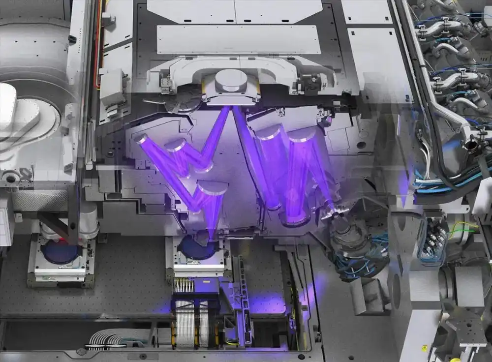
How deep the crack goes, no one knows right now. The technical level of that machine roughly corresponds to ASML's 2008 Twinscan NXT:1950i — numerical aperture 1.35, overlay accuracy 2.5nm, resolution 38nm.
That is, a gap of about eighteen years. It is primarily composed of domestic components, though some parts still rely on imports. SMIC began trial use in September 2025; the most optimistic projection is mass production in 2027.
Eighteen years.
To understand what eighteen years means, to understand why five machines could move forty-four billion dollars, one must first know how long this road has been.
Sixty-nine years, counting from when an American named it in an ordnance lab.
The Naming (1957)
In the autumn of 1957, at the US Army's Diamond Ordnance Fuze Laboratory, a young physicist named Jay Lathrop and his colleague James Nall were doing a laborious task.
They wanted to make transistors smaller to fit into mortar shell fuses. Manual work was not feasible; too large. Someone thought of a microscope — not for looking, but for projecting. Invert the microscope; the lens doesn't magnify, it reduces.
They coated a germanium wafer with Kodak photoresist, let light pass through a mask to project down, developed it, and etched. The pattern emerged.
Lathrop gave this process a name: photolithography, printing with light.
The military awarded them $25,000. Lathrop used his share to buy a station wagon for his family.
He was thirty that year. Sixty-nine years later, the thing he named became the most expensive, most difficult, and least accessible craft on Earth.
Pressing Close (1961–1972)
The earliest lithography machines were rudimentary. The mask was pressed directly onto the silicon wafer, with a vacuum drawn in between to keep it tight and prevent light distortion. This was contact lithography.
In the spring of 1961, GCA's David W. Mann division in the US launched the first commercial photo repeater — first reducing the mask, then printing it frame by frame onto a glass substrate. The first one was sold to Clevite Corporation. This machine didn't process wafers, only masks, but it was the ancestor of all subsequent steppers.
In 1965, Kulicke & Soffa launched the first commercial contact aligner. It nearly monopolized this (actually very small) market throughout the sixties.
Chip line widths back then were 200 micrometers — about as thick as two human hairs.
It was also at this level of technology that China entered the field. In 1966, the Chinese Academy of Sciences' 109 Factory and Shanghai Optical Instrument Factory collaborated to produce the Model 65 contact lithography machine, manufactured by Shanghai Radio Special Equipment Factory and promoted nationwide. China was five years late.
Five years was a catch-upable distance in that era.
Contact lithography had a fatal flaw: the mask wore out a little with each press, becoming useless after dozens of presses, and a single speck of dust meant a defect. Yield couldn't rise.
No Touch (1973)
In 1973, PerkinElmer launched the Micralign, the first commercial projection aligner. The mask no longer touched the wafer; a set of lenses sat in between, projecting at 1:1 magnification.
The result was revolutionary: yields jumped from 10% to 70%.
PerkinElmer became the world's largest semiconductor equipment supplier within three years. Ultimately, over two thousand Micraligns were sold.
Once something becomes this useful, its owner rarely wants to think about alternatives. This is the first instance of this pattern in this history, and it would appear three more times.
Step by Step (1977–1980)
The problem with projection lithography was that it illuminated the entire wafer at once. As wafers grew larger, lenses had to grow larger too, leading to thermal distortion. PerkinElmer's overlay accuracy was stuck around two micrometers.
GCA took a different path: don't expose the whole wafer, expose only a small area at a time, then move the stage one step and expose the next area. Hence the name 'stepper.' A small field of view allowed for small, high-numerical-aperture lenses, and also reduction projection — patterns on the mask could be ten times larger than on the wafer, lowering mask-making difficulty by an order of magnitude.
In 1977, a prototype was delivered to IBM. In 1978, the DSW 4800 was officially released: g-line light source, 10x reduction, Zeiss 0.28 NA lens, 10×10 mm field of view.
This machine established the basic architecture of lithography machines for the next half-century. Even ASML's most expensive machine today is, in terms of architecture, a descendant of the DSW 4800.
A frequently told anecdote: GCA almost used Nikon's lenses but chose Zeiss in the end, citing better field flatness. That decision, seen then as mere procurement, looks like industrial geography forty years later.
A DSW 4800 cost $500,000, over thirty times the price of PerkinElmer's projection machine. IBM, AT&T, Fairchild, National Semiconductor — these giants could afford it. Others could not.
Within Ten Years, America Lost It All (1980–1993)
Those who couldn't afford it were in Japan.
Nikon's NSR series followed the same path but did three things: brighter light source, larger field of view (5:1 reduction), and the addition of laser interferometer stages and automatic alignment. In plain terms — same precision, faster throughput.
In 1982, Nikon established Nikon Precision Inc. in Silicon Valley. It poached clients one by one from GCA: IBM, AT&T, Intel, RCA, Texas Instruments, AMD. By 1985, Nikon's revenue surpassed GCA's.
In 1984, Canon's first stepper, the FPA-1500FA, shipped. The domestic Japanese market absorbed a significant portion of global stepper output — according to Atsuhiko Kato's chronicle, nearly six hundred units of the global shipments that year stayed within Japan. The home market buoyed Canon.
The numbers changed like this: In 1980, American manufacturers held 90% of the global lithography market. By 1990, about 10% remained. GCA and Ultratech each held four to five points, SVGL about one point.
In 1990, PerkinElmer sold its lithography business to Silicon Valley Group (SVG). In 1993, GCA was dissolved — its parent company, General Signal, couldn't find a buyer. Its patents were transferred to a small company, later swallowed by Ultratech.
It's not that the US government didn't intervene. DARPA invested money, SEMATECH invested money, using taxpayer funds to bring GCA and PerkinElmer's machines back to a competitive level. But American chip companies wouldn't buy them. They had better relationships with Nikon and Canon, getting access to new machines earlier.
A question was asked even back then: If they didn't plan to buy, why should the government pay?
America wasn't blockaded out of this industry. It let go. It invented lithography, made the first photo repeater, the first projection machine, the first stepper, then withdrew within a decade.
The Dutch Shed (1984–2001)
In 1984, Philips and ASM International formed a joint venture called ASML, headquartered in a leaky shed on the Philips campus in Eindhoven.
The early years were rough. The first commercial stepper, PAS 2000/10, shipped in 1985, with Cypress Semiconductor as the main customer. In 1990, ASM International sold its shares and exited. In 1995, ASML went public on both the Amsterdam and Nasdaq exchanges, then holding about a quarter of the global market share — and mostly taking share from Americans, not the Japanese.
The real turning point came in 2001, with two events happening simultaneously.
First, the TWINSCAN platform was introduced. It had two wafer stages: while one wafer was being exposed, another was simultaneously being measured and aligned next to it, swapping positions directly after exposure. Physically, this split the machine in two; commercially, it nearly doubled throughput.
Second, ASML acquired Silicon Valley Group. SVG was the legacy of PerkinElmer and Intel's primary lithography supplier. Buying SVG gave ASML a ticket into Intel, and America completely exited lithography machine manufacturing.
Water (2002–2007)
Around 2000, the industry hit a wall.
The 193nm argon fluoride laser had reached its limit. The next step was universally considered to be 157nm fluorine lasers — shorter wavelength, finer lines. The whole world poured money into it. But 157nm light is absorbed by most materials, lenses had to use calcium fluoride, photoresist had to be redone, everything had to start over, and it was prohibitively expensive.
In 2002, a man named Burn Lin proposed another solution at a SEMATECH seminar. He was then Vice President of R&D at TSMC.
He said: Don't change the light source. Fill a layer of water between the lens and the wafer.
The refractive index of water is about 1.44. When 193nm light enters water, its effective wavelength becomes about 134nm — shorter than 157nm, and you don't have to change anything. Resolution improves by about 40%, at almost zero cost.
The idea was so simple that initially no one believed it. Water would have bubbles, leave watermarks, flow everywhere; how could it be inserted into a machine with nanometer precision?
ASML believed it. Philips Research had studied immersion lenses for high-density optical discs earlier and knew how to keep a layer of water stable under a lens. Zeiss modified the lens in Germany. In the autumn of 2003, the prototype TWINSCAN AT:1150i captured its first images.
The pace was rapid thereafter: The first commercial immersion machine, XT:1250i (NA 0.85), shipped to TSMC and IBM in 2004; XT:1700i (NA 1.2) in 2006, the first mass-production immersion machine; XT:1900i in 2007, numerical aperture 1.35.
1.35 — this number has never been surpassed since. The refractive index of water is the limit; physics ended there. For the next twenty years, every immersion DUV machine in the world maxed out at 1.35.
Nikon's first immersion prototype wasn't completed until October 2004, nearly two years late. Canon never produced one.
The entire industry's investment into the 157nm path was completely written off.
This is the second instance in this history: not technology defeating technology, but bets defeating bets.
Bringing the Sun into the Machine (1985–2019)
Optics reached its ceiling at 1.35. To go further, the light source had to be changed.
Extreme ultraviolet light at 13.5nm was first imaged by Japan's Hiroo Kinoshita in the mid-1980s, based on Soviet research on multilayer reflective mirrors from the 1970s.
This wavelength has a fatal property: it is absorbed by air, by glass, by almost everything. So lenses cannot be used, only mirrors; it cannot travel in air, the entire machine must be under vacuum.
In 1992, Intel invested $200 million, with funds mainly flowing to Sandia, Lawrence Livermore, and Bell Labs. In 1994, the US formed the National EUV Lithography Program, led by DARPA and the Department of Energy. In 1996, Congress cut the DoE funding.
In 1997, a SEMATECH-convened technology assessment ranked four next-generation paths. EUV came last, behind X-ray, electron beam, and ion projection lithography.
What happened next is well-known: the one that came last won. But it won extremely uglily — from being ranked last in 1997 to Samsung mass-producing 7LPP with EUV in October 2018 and TSMC's N7+ following in Q2 2019, twenty-one years passed.
Key milestones:
2006: ASML delivered the first EUV prototype, with a light source too weak to be usable.
2010: The first NXE:3100 was delivered to Samsung, achieving "first light" on Christmas Eve.
2012: Intel, TSMC, and Samsung participated in the Customer Co-Investment Program, providing funds, five-year R&D commitments, and purchasing ASML shares.
2013: ASML acquired the light source company Cymer for $2.5 billion.
2016: The NXE:3400 began receiving bulk orders, marking an inflection point.
Early 2020: The 100th EUV machine shipped.
How is the light generated? A tin droplet flies in a vacuum, struck sequentially by two carbon dioxide lasers — the first flattens it, the second vaporizes it into plasma, radiating 13.5nm light. Fifty thousand times per second.
This machine has over 100,000 parts. Shipping one requires forty containers, three cargo planes, twenty trucks. ASML invested over six billion euros in EUV R&D.
December 2023: The first High-NA machine, the EXE, was delivered, increasing the numerical aperture from 0.33 to 0.55.
The prices are: the current Low-NA EUV, about 170 million euros per machine. The High-NA EXE, about 350 million euros. The latter weighs 150 tons, requires 250 crates for transport, and 250 engineers working for six months for installation.
One machine costs as much as a wide-body airliner. And only a few dozen are produced each year.
The Shape of Monopoly
The current state: EUV, only ASML in the world can make it. Immersion DUV, ASML holds about 98.7%. Nikon is still around but has only scattered shares in mature processes. Canon left long ago, switching to nanoimprint.
2025: ASML revenue was 32.7 billion euros. The Chinese market once accounted for 41% (2024), dropped to 33% in 2025, and is projected to be about 20% in 2026.
Epilogue: The True Pattern of This History
Compressing sixty-nine years into one sentence: it is not a history of invention.
It is a history of "who was nurtured by customers."
Four relays, four times it was not technology losing to technology:
PerkinElmer didn't fail to understand steppers; its projection machines were just selling too well. GCA's product wasn't bad; American chip companies refused to buy American machines. Nikon didn't fail to make immersion machines; it bet on 157nm, and the people making that call were not on the customer's production line. ASML survived because in 2012, TSMC, Intel, and Samsung were willing to put money and shares into a machine that didn't yet work.
A lithography machine's iteration cycle is ten years. No equipment company can survive on its own cash flow for ten years. It must be nurtured. Those nurturing it must tolerate its initial shortcomings, place orders, and send engineers into the other's factory.
This is why lithography has never been a question of "can it be built."
Prototypes can be made by anyone. Shanghai made one in 1966. In 1985, when the Institute 45 of the Ministry of Machinery and Electronics' step-and-repeat projection lithography prototype passed the Ministry of Electronics' appraisal, the appraisal opinion stated its performance was close to the American GCA's 4800DSW — this claim comes from domestic industry recollections, lacking first-hand technical documentation for verification, but even discounting it, the gap was measurable in years, not generations.
The question has always been: After it's built, who will use the first, not-yet-good one? Who will use the second, still-not-great one? Who will use it up to the tenth?
America had invention but didn't hold onto this patience. Japan had patience but bet wrong on one direction. The Netherlands had nothing — no silicon fabs, no chip design, a land area smaller than a province — but its three customers were willing to endure twenty-one years with it.
A beam of light walked for sixty-nine years. What walked the full distance was never the light.
——·END·——
Original article No.7013 | Author Zhou Luoshi
Sources: Chronology & Technical Details: Atsuhiko Kato, Chronology of Lithography Milestones (lithoguru.com) — main timeline of this article; Chris Mack, Milestones in Optical Lithography Tool Suppliers (lithoguru.com); Computer History Museum, The Silicon Engine: 1955/1957 Lathrop and Nall entries; ASML official history: Our history / Making EUV: from lab to fab / TWINSCAN: 20 years; Jay W. Lathrop, "The Diamond Ordnance Fuze Laboratory's Photolithographic Approach to Microcircuits," IEEE Annals of the History of Computing, 35(1), 2013; Flagello & Arnold, "Optical Lithography for Nanotechnology," Proc. SPIE 6327
Industry History & Analysis: Chris Miller, Chip War (2022); Rebecca Henderson, "Of Life Cycles Real and Imaginary: The Unexpectedly Long Old Age of Optical Lithography," Research Policy 24 (1995) — explains why PerkinElmer couldn't hold on; Brian Potter, "How ASML Got EUV," Construction Physics (2025); Jon Y (Asianometry), "How Japan Won the Lithography Industry" / "A Deep Dive into Immersion Lithography"; Van Atta et al., "The Tunnel at the End of the Light," Issues in Science and Technology; MIT Technology Review, "The chip patterning machines that will shape computing's next act" (2023)
China Section: History of the Institute of Microelectronics of the Chinese Academy of Sciences (109 Factory 1958–1986)
Current Data: ASML 2025 Annual Report and Q1 2026 Earnings Call; Caixin / SCMP reports on ASML's China revenue share (Jan, Apr 2026)
This article comes from the WeChat public account: Qin Shuo Circle of Friends , Author: Zhou Luoshi