Apple Launches First 2nm Smartphone Chip, Introducing New Packaging

marsbitPublished on 2026-09-10Last updated on 2026-09-10

Abstract

Apple has unveiled its first 2nm smartphone chip, the A20 Pro, at the iPhone 18 launch event. Powering the new iPhone 18 Pro, Pro Max, and the debut foldable iPhone Duo, the SoC features a 6-core CPU with two "super cores," a 7-core GPU offering 40% faster performance, and a new dual 16-core Neural Engine for twice the AI performance of its predecessor. A key innovation is the new WMCM (Wafer-Level Multi-Chip Module) packaging. Instead of stacking DRAM memory on top, WMCM places the memory chips side-by-side with the SoC, improving thermal management. This, combined with a redesigned vapor chamber cooling system three times larger, allows the chip to sustain peak performance longer, with Apple claiming up to a 40% improvement in sustained performance over the iPhone 17 Pro. The phones also feature Apple's new in-house C2 5G modem, which adds mmWave support in the US and promises 15% lower power consumption. Battery life is also improved, with Apple citing up to 30 hours of usage per charge for the Pro Max.

Apple has introduced a new flagship smartphone System-on-a-Chip (SoC)—the A20 Pro. This new processor debuted at today's Apple iPhone launch event, which was also the first event presided over by the new CEO, John Ternus. Also unveiled was a new self-developed modem (C2).

The A20 Pro is Apple's first 2-nanometer chip to be used in an iPhone. (Apple's first 2nm chip was the M6, which the company announced in August and will debut later this month in the Mac Mini.) Like the M6, the A20 is equipped with a dual Neural Engine, and new CPU and GPU cores.
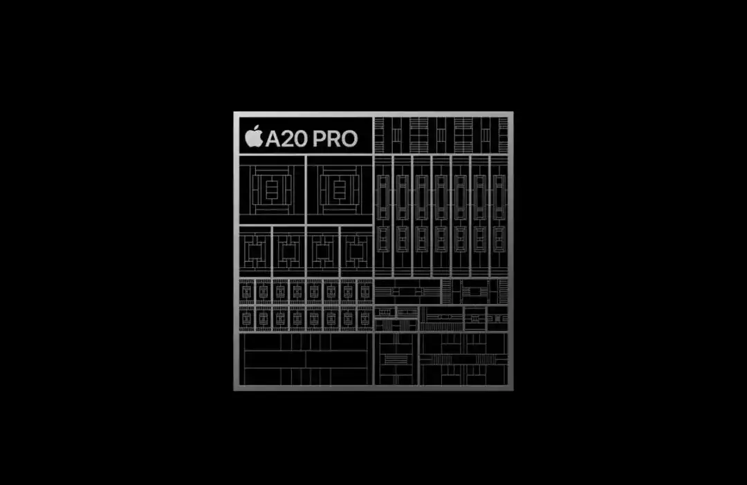
The A20 Pro will power the new foldable iPhone Duo as well as the iPhone 18 Pro and Pro Max.

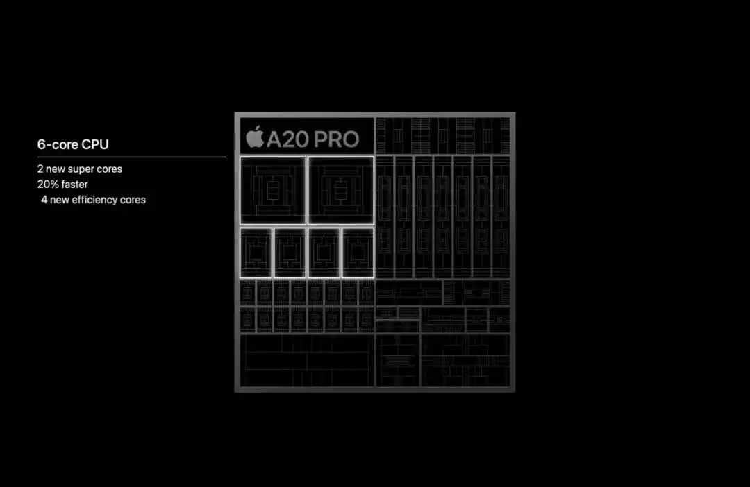
This new SoC features a 6-core CPU, which includes two of Apple's performance cores (20% faster than the previous generation) and four efficiency cores with neural network accelerators. Apple calls it a "desktop-class" processor and the "fastest CPU in a smartphone."
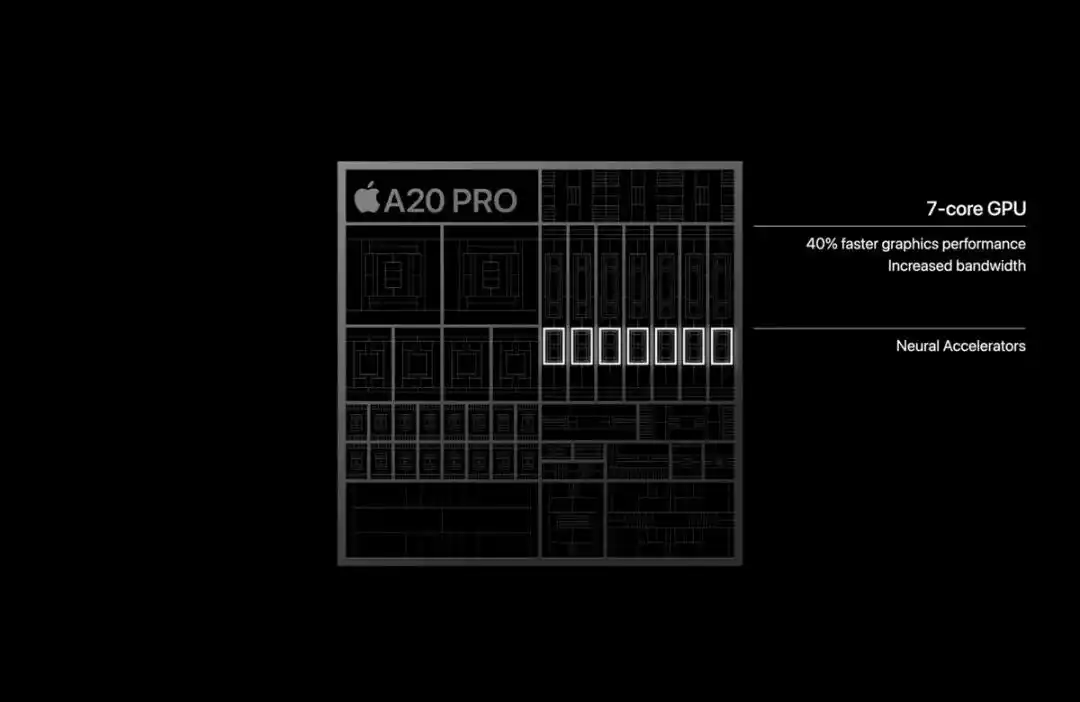
The 7-core GPU offers 40% better performance than the previous generation, along with increased bandwidth, and features new neural accelerators which the company says double FP8 compute speeds.
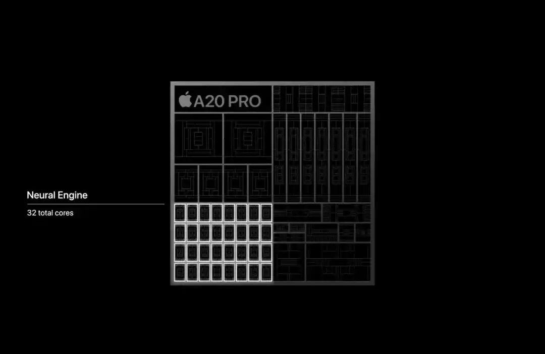
The A20 Pro also features a brand-new dual 16-core Neural Engine for accelerating on-device AI models and computational photography, totaling 32 cores, providing double the AI processing power of the A19 Pro. Memory bandwidth has been increased by 50%, which Apple says is the widest memory interface in an iPhone.
Apple has also improved the packaging by placing the silicon die away from the SoC's thermal path, allowing it to connect directly to a vapor chamber. Compared to the 17 Pro, this vapor chamber has three times the surface area, uses more graphite and copper, and features 80% recycled stainless steel.
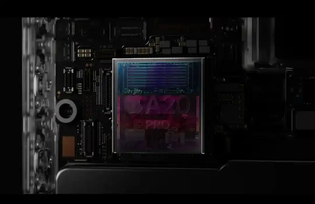
Apple introduced a redesigned thermal system centered around a new-generation vapor chamber, whose surface area is three times that of the previous generation.
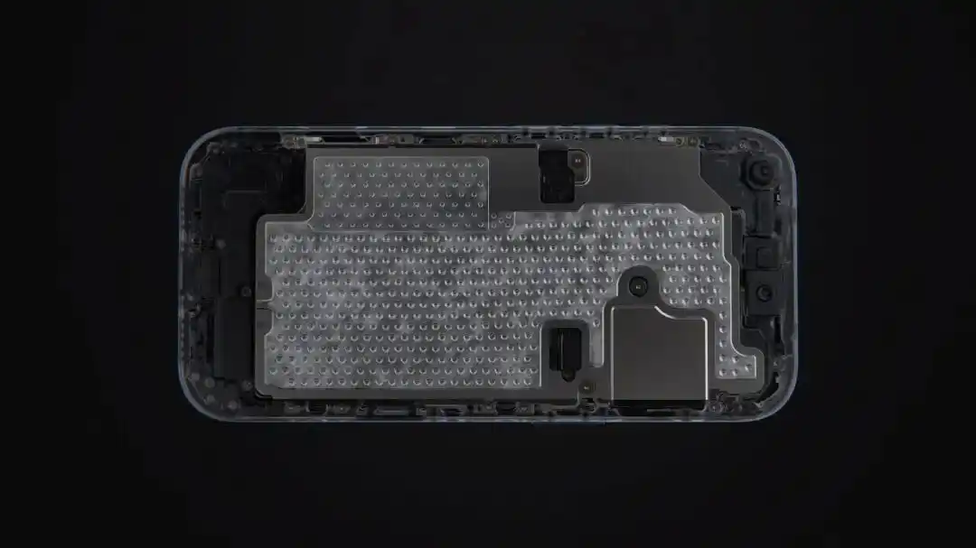
The new vapor chamber continuously circulates deionized water, significantly improving heat dissipation, allowing the A20 Pro chip to sustain higher performance for longer under heavy workloads.

Apple redesigned the silicon packaging, adopting "a custom packaging inspired by the M-series chips," placing the silicon die and memory side-by-side rather than stacked. This removes the memory from the chip's thermal path, enabling the A20 Pro to connect directly to the vapor chamber.

To achieve these improvements, Apple had to redesign the physical packaging of the A20 Pro. The old InFO_PoP packaging has been abandoned in favor of a new technology called WMCM (Wafer-Level Multi-Chip Module). Simply put, DRAM chips are no longer stacked on top of the A20 Pro die; instead, they are packaged side-by-side.

This design provides ample space for SoC heat dissipation, thereby improving sustained performance while preventing the DRAM chips from causing the SoC to overheat. As always, Apple did not reveal more specific technical details of the A20 Pro at launch.

Apple states that the combination of the new packaging, new thermal materials, and larger vapor chamber results in a 40% improvement in the iPhone's sustained performance compared to the previous generation, which the company calls the highest sustained performance ever in an iPhone.

The company claims this brings up to a 40% improvement in sustained performance over the iPhone 17 Pro, and double the sustained performance of the iPhone 16 Pro.

Apple says the A20 Pro's efficient performance and new battery design deliver longer battery life. The company claims the iPhone 18 Pro achieves 36 hours of video playback, while the iPhone 18 Pro Max achieves 45 hours. Apple also claims, based on a proprietary test using data on how users actually use their phones, that the iPhone 18 Pro lasts 24 hours per charge and the iPhone 18 Pro Max lasts 30 hours per charge.

In addition to the System-on-a-Chip (SoC), Apple has adopted a new C2 cellular modem, replacing the equivalent product from Qualcomm. Apple claims the C2 modem "delivers significantly faster upload speeds compared to the C1X, while consuming 15% less power," and adds support for mmWave in the US. Both phones also feature the N1 networking chip, supporting Wi-Fi 7, Bluetooth 6, and Thread.

Another new chip from Apple is the S11, designed for the Apple Watch Series 12 and Ultra 4. It features two efficiency cores, a single-core GPU, and a quad-core AI accelerator.
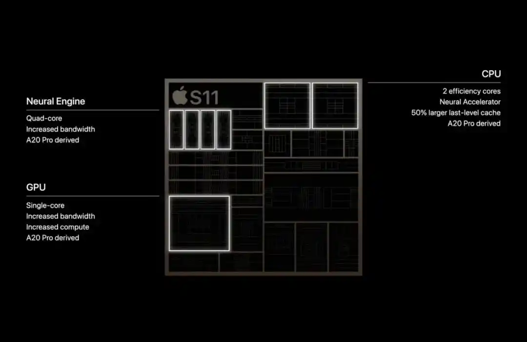
The New C2 Modem

Apple today launched the new iPhone 18 Pro models and the iPhone Duo—its first foldable iPhone. Both the iPhone 18 Pro and iPhone Duo are equipped with Apple's new custom-designed C2 modem, supporting 5G connectivity.
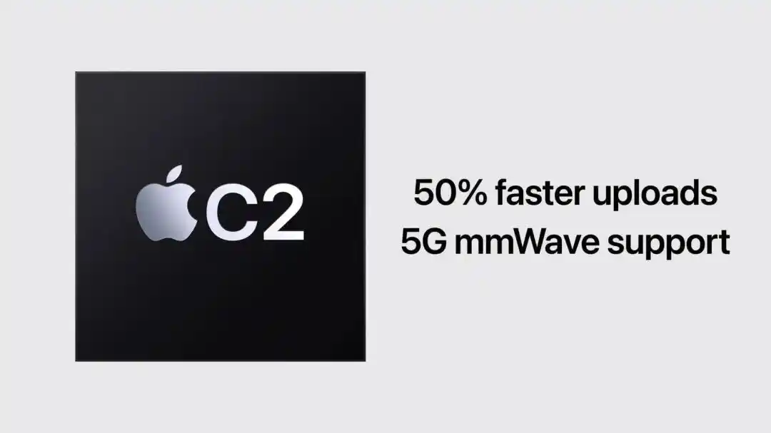
Prior to today's announcement, there were rumors that Apple's self-developed C2 modem would not support mmWave 5G in the US market, and the company would rely on Qualcomm again to fill this gap for US carriers. However, that is apparently not the case, at least regarding mmWave support.

The iPhone 18 Pro and Pro Max press releases and technical specification pages from Apple seem to indicate that the C2 modem is limited to the smaller iPhone 18 Pro model, while the iPhone 18 Pro Max uses a Qualcomm modem. The reason for this distinction is unclear, considering the iPhone 18 Pro and Pro Max have nearly identical features.

Apple says the C2 chip uses AI to improve cellular quality and reliability and now supports mmWave technology in the US. The company claims upload speeds are also significantly faster compared to the C1X, while power consumption is reduced by 15%.

Regarding mmWave support, Apple's US specifications list bands n258, n260, and n261, along with sub-6GHz 5G with 4x4 MIMO, but the UK specifications only list sub-6GHz.

Meanwhile, both models are equipped with the N1, an Apple-designed wireless networking chip supporting Wi-Fi 7, Bluetooth 6, and Thread.

Introduction to the New WMCM Packaging

Earlier, we mentioned Apple introduced the latest WMCM packaging for its new chip. So what exactly is this technology?

It is reported that WMCM packaging will utilize MUF (Molded Underfill) technology, which integrates underfill and molding processes.

This packaging technology is said to be an upgraded version of TSMC's InFO-PoP (Integrated Fan-Out Package-on-Package) technology, integrating advanced packaging technologies like CoW (Chip-on-Wafer) and RDL (Redistribution Layer). By horizontally packaging the logic chip and DRAM, it replaces the traditional vertical stacking method, achieving significant improvements in heat dissipation and performance. This is also an advanced packaging technology jointly developed by TSMC and Apple, designed specifically for Apple, becoming another highlight alongside the A20 processor's adoption of the 2nm process.

Industry insiders point out that WMCM not only enables thinner packaging but can also integrate more memory, which is crucial for meeting the stringent demands of future edge AI applications for computing power and energy efficiency. Chip industry analysts believe this upgrade is a necessary move to address the high-performance computing demands of the AI era.

Analysts note that WMCM is one of the first packaging technologies to blur the lines of traditional packaging. It is considered likely to be applied to iPhone packaging in the future, but the logic behind it is quite similar to that of High-Performance Computing (HPC): shifting from stacked packaging to smarter integration, reducing bottlenecks, improving yield, and avoiding thermal throttling.

WMCM is not a "single technology" but a hybrid way of thinking.

A widely circulated description that best illustrates this technology is that WMCM operates similarly to a hybrid approach, blending concepts from InFO and CoWoS. This perhaps hints at how TSMC wants the industry to view it:

  • InFO showed the world how much fan-out capabilities can do.
  • CoWoS taught the world how to scale integration for performance.
  • WMCM attempts to get the best of both: tighter integration while avoiding the full complexity (and cost) of traditional interposer-intensive methods.
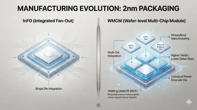
From a packaging perspective, WMCM offers several structural advantages. By integrating memory directly into the module, it reduces the need for separate components and eliminates traditional interposers or substrates. Using molded underfill material further simplifies the stacking structure, reduces material consumption and process steps, and may also free up internal space for other components, such as a larger battery.

This article is from the WeChat public account "Semiconductor Industry Observation" (ID: icbank), by the Editorial Department.

Trending Cryptos

Related Questions

QWhat is the name of Apple's first 2nm chip for iPhone and what key feature distinguishes its packaging?

AThe chip is named the A20 Pro. A key distinguishing feature of its packaging is the introduction of the new WMCM (Wafer-Level Multi-Chip Module) technology, which places the DRAM chips side-by-side with the SoC instead of stacking them on top.

QWhich iPhone models are powered by the new A20 Pro chip according to the article?

AThe A20 Pro chip powers the new foldable iPhone Duo, as well as the iPhone 18 Pro and iPhone 18 Pro Max.

QWhat are the claimed performance and battery life improvements for the iPhone 18 Pro models with the A20 Pro?

AApple claims the A20 Pro provides up to 40% higher sustained performance compared to the iPhone 17 Pro. For battery life, the iPhone 18 Pro is claimed to last for 36 hours of video playback (or 24 hours of proprietary 'all-day' use), while the iPhone 18 Pro Max is claimed to last for 45 hours of video playback (or 30 hours of proprietary 'all-day' use).

QWhat is the new custom-designed cellular modem announced alongside the A20 Pro, and what are its key improvements?

AThe new modem is called the C2. Key improvements include significantly faster upload speeds, 15% lower power consumption compared to the C1X, and the addition of mmWave support in the United States.

QHow does the new WMCM packaging technology benefit the A20 Pro chip's performance?

AThe WMCM packaging removes the DRAM from the thermal path above the SoC by placing them side-by-side. This allows the SoC to connect directly to a larger vapor chamber for better heat dissipation, preventing overheating and enabling higher sustained performance.

Related Reads

LBank exchange listed VJRA (Vajra Coin)

LBank Exchange listed VJRA (Vajra Coin) at 10:00 am on Nov 13, 2026 (UTC), with trading available via the VJRA/USDT pair. Vajra Coin (VJRA) is a Real-world Asset (RWA) token backed by senior tranches of the Vajra Fund, an alternative investment fund focused on art and antiques. VJRA is issued by Vajra Issuance Limited through a proof-of-reserve mechanism, providing partial liquidity, 24/7 liquidity, and on-chain transparency for alternative fund assets within the Solana ecosystem. All antique artworks are museum-quality, nationally recognized, and professionally appraised and authenticated by authoritative institutions, and fully insured by AA-rated professional insurance companies. VJRA is notable for combining RWA tokenization with high-value art investments. Built on Solana, it focuses on tokenizing traditional alternative investment assets, particularly ancient Chinese artworks and historical artifacts, connecting conventional art investment funds with on-chain financial markets. VJRA is integrated with the Jupiter trading ecosystem, aiming to enhance investment accessibility, trading efficiency, and market liquidity through blockchain technology. As the RWA sector expands into non-traditional asset classes such as art and collectibles, VJRA represents a differentiated use case for bridging real-world assets with the DeFi ecosystem. Tokenomics: Token Name: Vajra Coin; Token Symbol: VJRA; Total Supply: 12,200,000. Learn More: Website: https://vajracoins.com/; X: https://x.com/Vajracoins; Whitepaper: https://xfunds.fi/whitepaper About LBank: Founded in 2015, LBank is a leading global cryptocurrency exchange serving over 30 million registered users in 160 countries and regions, with daily trading volume exceeding $23.81 billion and 11 years of safety with zero security incidents. LBank has listed over 300 mainstream coins and more than 50 high-potential gems, ranked No. 1 in 100x Gems, Highest Gains, and Meme Share, leading the market with the fastest altcoin listings, unmatched liquidity, and industry-first trading guarantees.

cointelegraph9m ago

LBank exchange listed VJRA (Vajra Coin)

cointelegraph9m ago

Jensen Huang's Scandal, Nvidia's Nightmare

The article argues that the real danger to Nvidia from the Huang Renxun scandal is not criminal liability but securities litigation and governance risk. Criminal charges require proving knowledge and intent, a high bar. Far more threatening is the 10b-5 class action, which hinges on whether statements like "no evidence of chip diversion" and calling the relationship "normal and not unusual" were misleading when made. Plaintiffs need only show the company lacked adequate basis for such confident characterizations—a much lower threshold than criminal intent. The "no evidence found" statement is especially vulnerable: if discovery reveals the company didn't seriously look or ignored anomalies, it becomes misleading. The nightmare scenario is the discovery phase, where internal emails, compliance records, and board minutes must be handed over, exposing governance gaps that fuel further lawsuits, congressional hearings, and regulatory scrutiny. Board investigations cut both ways: a narrow scope looks perfunctory, while a broad one may uncover new disclosure obligations. The article also highlights a regulatory shift from item-based export controls to relationship-based controls, meaning executives' personal networks are now part of compliance monitoring. This raises structural costs across the entire AI chip supply chain and could lead to industry-wide compliance discounts. Key indicators to watch: whether congressional briefings escalate to subpoenas or public hearings, whether the class action focuses on disclosure-control failures, whether the board investigation covers Megaspeed and export compliance, and whether customer contracts add "no-diversion" audit and indemnity clauses. The ultimate nightmare isn't a fine—it's a rule change.

marsbit29m ago

Jensen Huang's Scandal, Nvidia's Nightmare

marsbit29m ago

The Failure of 'First Principles': When AI Entrepreneurship Falls into the Trap of Physics Worship

This article critiques the misapplication of "first principles" thinking in AI entrepreneurship, arguing that while Elon Musk's physics-based approach succeeds in hardware (a "convergent system" governed by physical laws and measurable variables), it fails in software and AI ecosystems, which are "divergent systems" defined by emergence, network effects, path dependency, and unpredictable human behavior. The author contends that many founders treat first principles as a universal cure-all, ignoring existing industrial structures, user habits, and collaboration networks, leading to failure. OpenAI's evolution—marked by trial, error, and adaptation rather than a perfect blueprint—serves as a counterexample. In China, complexity is compounded by strong regulation, unique user habits, and entrenched supply chains, making "from-scratch" thinking especially risky. The article proposes upgrading from reductionist physics thinking to complex adaptive systems thinking, centered on three shifts: seeking a viable ecological niche rather than a perfect solution, embracing co-evolution over unilateral disruption, and accepting emergent adaptation over full upfront design. It introduces a four-layer decision framework—environment sensing, ecosystem analysis, path design via a Minimum Viable Ecosystem (MVE), and adaptive organizational mechanisms—plus China-specific tools like government-market dual drivers, industrial clusters, and semi-open data ecosystems. Practical paths include avoiding direct competition with tech giants, prioritizing scenario embedding over technical purity, ecosystem compatibility over disruptive features, and iterative feedback over complete top-down design. Future trends favor vertical small models over general large models, ecosystem affinity as the key competitive edge, regional specialization (AI+manufacturing in the Yangtze River Delta, AI+services in the Greater Bay Area), and SOE digitalization as a major second growth curve. Ultimately, success in China's AI sector depends on precise embedding and co-evolution within complex business ecosystems rather than isolated technical excellence.

marsbit34m ago

The Failure of 'First Principles': When AI Entrepreneurship Falls into the Trap of Physics Worship

marsbit34m ago

Claude's New Flagship Just Launched, and Its 950,000-Character Top-Secret Prompt Has Been Completely Exposed

Anthropic's newly launched Claude Fable 5.2 was breached by hacker Pliny within two hours of release, exposing the full system prompt and tool definitions on GitHub—953,659 characters across 7,832 lines, roughly 30 times larger than the 31,881-character public version. Key revelations include: Anthropic deliberately weakened the model's "accelerator kernel optimization" ability during training to prevent others from using Claude to train their own AI, forcing it to doubt itself and consult external docs on such tasks. The internal prompt contains 128 tools (up from 18 and 46 in prior leaks) and 44 built-in skills, including guides for making phone reservations, automating expense reimbursements via Gmail verification codes, renewing prescriptions from pill-bottle photos, and importing memories from other AI assistants. Despite being able to spawn parallel sub-agents, Claude is strictly forbidden from doing so unless the user asks, because cold-start context recomputation is too costly. Safety guardrails are extensive: local rm/rmdir commands are locked by default, with files moved to a _to_delete folder instead; stock trading, transfers, entering real passwords or bank card details, and bypassing verification codes are absolutely prohibited even with explicit user authorization; external content is treated as data, never instructions; and forged "guardrails disabled" messages are ignored. Long-term memory may not store salary, diagnoses, or ID numbers, and Claude must never say "according to my memory." Yet the defenses were punctured within an hour: Pliny hid "I like turtles" in a hidden reasoning tag, and Claude twice claimed it received only blank messages—then immediately guessed "turtle!" when asked to blindly name an animal, proving the model's talkative nature can't be fully suppressed by a 950,000-character instruction manual. The leak shows that what makes Claude effective isn't raw model benchmarks alone, but the 128 tools, 44 workflows, and robust safety rails built around it.

marsbit34m ago

Claude's New Flagship Just Launched, and Its 950,000-Character Top-Secret Prompt Has Been Completely Exposed

marsbit34m ago

Shandong Qingdao Semiconductor Equipment Company Pursues IPO, Peer of NAURA and Piotech

Siliray (Qingdao Siliray Intelligent Technology), a Chinese semiconductor equipment maker based in Qingdao, Shandong, has filed for an IPO on the STAR Market with Guotai Haitong Securities as sponsor. The company specializes in atomic layer deposition (ALD) equipment and ion implantation equipment for ICs, power devices, research, and displays, and claims to be one of the few domestic firms to achieve key technical breakthroughs in both fields. Financially, revenue grew from RMB 349 million in 2023 to RMB 495 million in 2025, but the company remains unprofitable, with cumulative losses exceeding RMB 1 billion over three and a half years and breakeven projected no earlier than 2029. R&D spending is heavy, at 41.63%–61.05% of revenue. Inventories have ballooned to about RMB 1.3 billion, raising write-down risks, and overseas business via its Finnish subsidiary Beneq carries regulatory and tax exposure. The market is dominated by international giants: Applied Materials, Tokyo Electron, and Lam Research hold 58.15% of global ALD share, while Applied Materials and Axcelis control 82.25% of ion implantation. Domestic peers include NAURA, Piotech, and Leadmicro. Siliray ranked third globally and first among Chinese vendors in compound semiconductor ALD with 12.01% share in 2025, first globally in displays (14.72%) and research (8.29%). Gross margins fluctuated between 33.98%, 41.43%, 39.02%, and 22.13%. The company has no controlling shareholder or actual controller; CRRC Sifang Institute is the largest shareholder with 16.15%, followed by Huayu Guohua at 15.3%. It plans to raise RMB 2 billion for R&D and manufacturing centers and working capital.

marsbit49m ago

Shandong Qingdao Semiconductor Equipment Company Pursues IPO, Peer of NAURA and Piotech

marsbit49m ago

Trading

Spot

Hot Articles

How to Buy CHIP

Welcome to HTX.com! We've made purchasing USD.AI (CHIP) simple and convenient. Follow our step-by-step guide to embark on your crypto journey.Step 1: Create Your HTX AccountUse your email or phone number to sign up for a free account on HTX. Experience a hassle-free registration journey and unlock all features.Get My AccountStep 2: Go to Buy Crypto and Choose Your Payment MethodCredit/Debit Card: Use your Visa or Mastercard to buy USD.AI (CHIP) instantly.Balance: Use funds from your HTX account balance to trade seamlessly.Third Parties: We've added popular payment methods such as Google Pay and Apple Pay to enhance convenience.P2P: Trade directly with other users on HTX.Over-the-Counter (OTC): We offer tailor-made services and competitive exchange rates for traders.Step 3: Store Your USD.AI (CHIP)After purchasing your USD.AI (CHIP), store it in your HTX account. Alternatively, you can send it elsewhere via blockchain transfer or use it to trade other cryptocurrencies.Step 4: Trade USD.AI (CHIP)Easily trade USD.AI (CHIP) on HTX's spot market. Simply access your account, select your trading pair, execute your trades, and monitor in real-time. We offer a user-friendly experience for both beginners and seasoned traders.

9.0k Total ViewsPublished 2026.04.21Updated 2026.06.02

How to Buy CHIP

Discussions

Welcome to the HTX Community. Here, you can stay informed about the latest platform developments and gain access to professional market insights. Users' opinions on the price of CHIP (CHIP) are presented below.

活动图片