玻璃基板突然加速

marsbitPublicado a 2026-06-25Actualizado a 2026-06-25

Resumen

AI算力行情轮动至玻璃基板领域。5月下旬,京东方与康宁就玻璃基板签署合作备忘录,引发资本市场强烈关注,带动彩虹股份、五方光电等相关公司股价大涨。英特尔与台积电两大芯片巨头正积极推动玻璃基板技术,旨在替代传统芯片封装中的部分载板材料,以解决AI芯片尺寸增大带来的散热翘曲问题并降低成本。英伟达宣布其下一代GPU Rubin将采用玻璃基板封装,显著加快了该技术的商业化进程。与此同时,显示面板产业凭借其成熟的玻璃基板加工技术与产线基础,成为推动该技术落地的重要力量,例如中国台湾的群创和大陆的京东方均已布局相关产线并取得进展。尽管特种玻璃材料、精密加工等关键技术挑战仍需攻克,大规模量产预计最早在2027年末实现,但玻璃基板已成为AI算力发展关键产业链中备受瞩目的新环节。

AI算力行情波浪式推进,涨完你的涨他的,现在轮到了玻璃基板。

5月下旬,京东方宣布与康宁就玻璃基板签订合作备忘录,彻底引爆行情。

不仅自家稳如心电图的股价垂直拉升“惊坐起”,连续两个交易日涨停,连带着彩虹股份、五方光电等上游公司一字涨停,帝尔激光股价创下历史新高,沃格光电近两个月累计大涨3倍。

机构将2026年判定为玻璃基板商业化验证元年。除了京东方和康宁的合作外,英特尔宣布在最新服务器CPU上成功量产玻璃核心基板,台积电透露玻璃基板CoPoS封装试产线建立。

两大巨头抓紧猛干,大涨气氛铺垫到位。

不得不说,玻璃基板的商业化速度,已经超过了绝大部分人的预期。

替代芯片中的“板”

英特尔和台积电是当前玻璃基板的头号旗手,但两家所说的“玻璃基板”,其实不完全是一回事。

一颗芯片由各类元器件组成,元器件被固定在载板上,构成一个功能单元,这些功能单元又被固定在下一层载板上,构成一个更大的功能单元,以此类推,呈现层级架构,

比如我们最熟悉的电路板,就是最底下一层的载板,再往上拆,还有核心基板、IC载板等等。

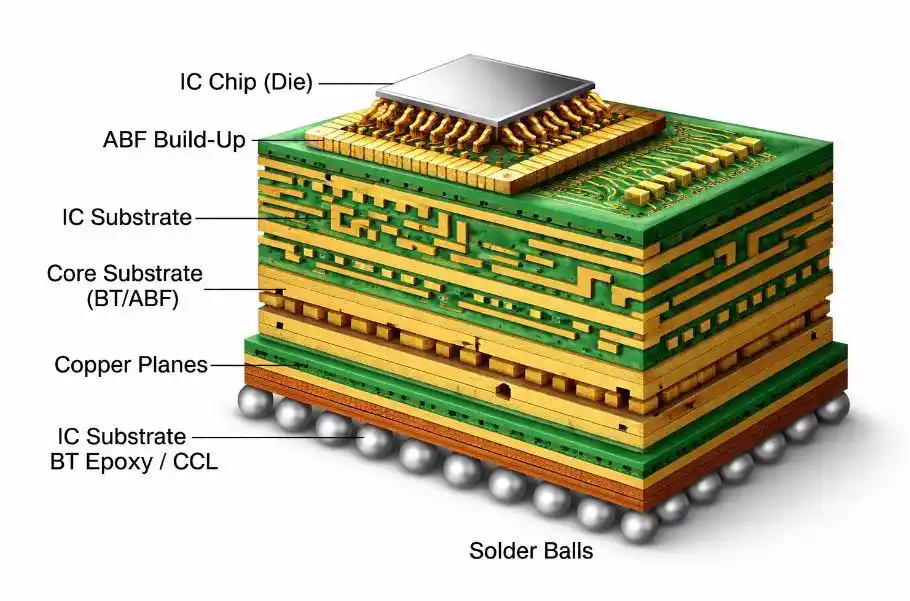
芯片内部不同层级的“板”;图片来源:IC Components

这些载板过去大部分由树脂、玻璃纤维、铜箔、硅等材料构成,而玻璃基板顾名思义,就是以玻璃为主要材料的基板。

英特尔和台积电想做的就是用玻璃基板取代主流载板,但替代的不是同一块“板”。

英特尔的“先进封装玻璃基板”,全名“玻璃核心基板”(Glass Core Substrate),替代的是电路板与芯片之间的那层IC载板。
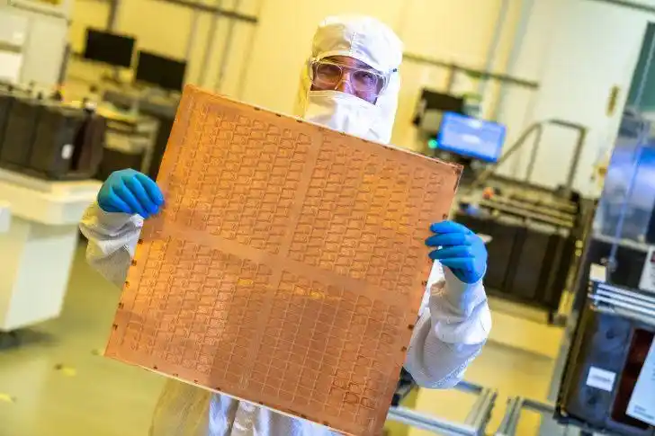
英特尔展示的一块测试用的玻璃核心基板

目前包括英伟达GPU在内的主流AI芯片,用的是以ABF材料为主的基板,最大缺点是受热易弯曲变形,一块一米长的ABF载板,每升高1°C就会膨胀约15微米。

与之相对的是放在ABF载板上面的硅芯片,受热时几乎不发生形变。

于是,当芯片在工作中产生热量,底部的ABF基板受热向外膨胀,上层的硅芯片却保持不变,整块基板就会发生弯曲,也就是“翘曲”。

芯片尺寸越大,翘曲就越严重,想象一张信用卡四个角同时拱起的样子。后果可能是灾难性的。

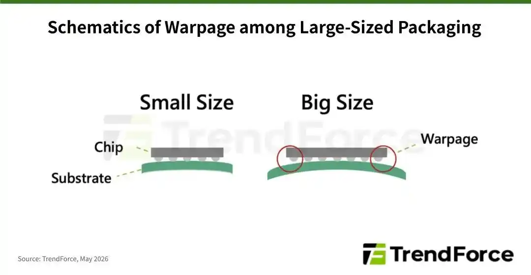
载板尺寸越大,翘曲越明显;图片来源:TrendForce

玻璃基板因此被抬上桌,由于其“耐热能力”与硅芯片相当,高温下即使形变,也能与硅芯片保持同步,就能有效避免翘曲。

与英特尔相比,台积电想要替代的载板位于更上一层——芯片的裸片层。

一颗GPU裸片由计算核心单元(CPU/GPU)和多颗HBM构成,被放置在硅中介层,这个硅中介层就是台积电最想要替代的那块板。

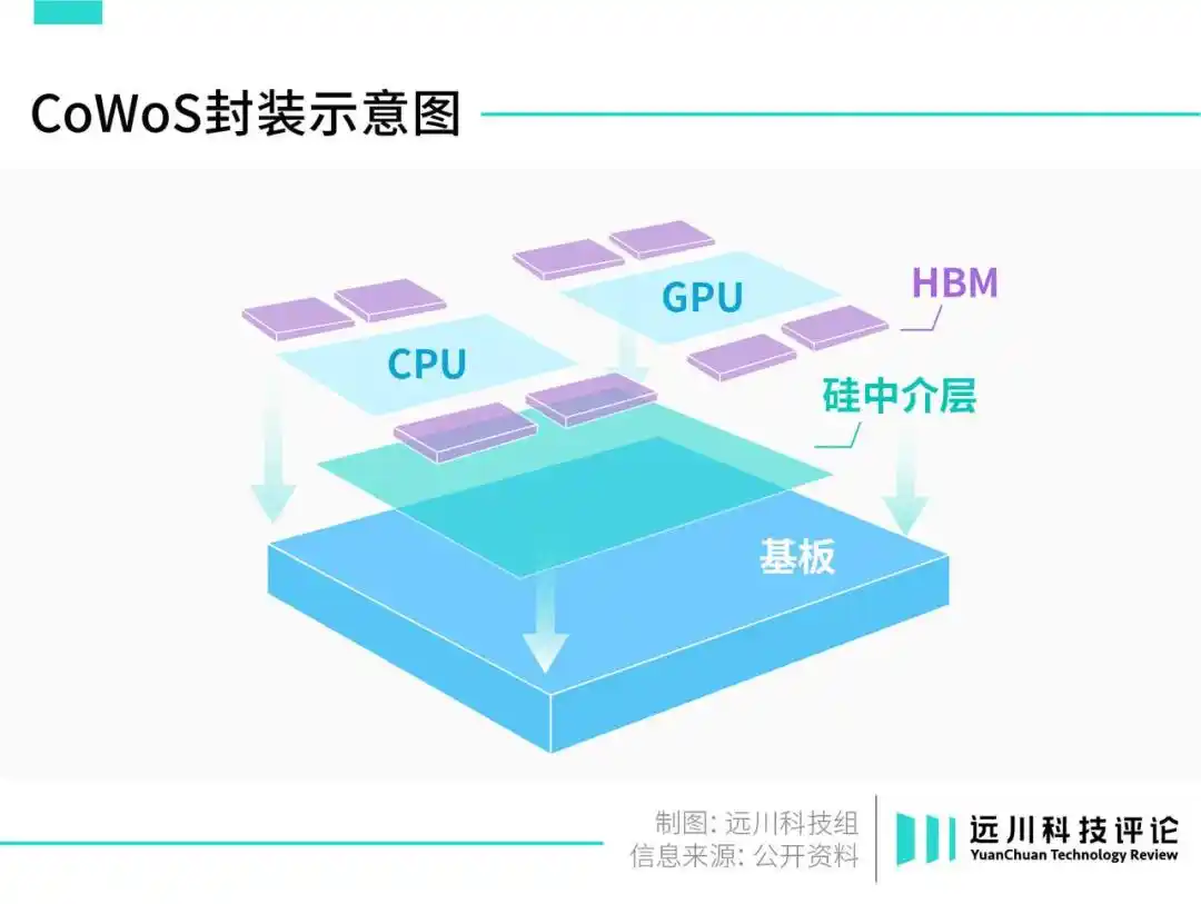
硅中介层制造成本极高,一块大尺寸硅中介层单价超过100美元[2]。作为对比,iPhone 17 Pro Max的A19 Pro,单颗采购价不过90美元。

而且相比于这些计算能力强大的手机SoC,硅中介层最大的作用只是数据搬运,相当于用跑车的价钱买了辆小电驴,听起来更亏。

硅中介层的大小与AI芯片的尺寸、HBM用的颗数直接相关。随着AI芯片越做越大,HBM越用越多,投入到硅中介层的成本黑洞也越挖越大。

对于购买AI芯片的厂商来说,相当于用10万块钱买了车,还得另花5万块钱买车牌才能上路。

用玻璃基板替代硅中基层,最大的好处就是便宜,同样尺寸,成本还不到后者的一半[2]。

英特尔和台积电的想法都很合理,但新技术的落地从来不是一声令下的事。尤其是在芯片行业,新技术挑战的不只是物理定律。

芯片制造是人类迄今为止最复杂的活动,在过去的半个多世纪固化下来了一套极度严苛的规则,上下游严丝合缝构建出了一套标准体系,牵一发而动全身。

再微小的调整,都可能牵连到上游的设备、材料的调整甚至推倒重来。

所以巨头们嘴上大胆创新,行动上却保守谨慎。

英特尔2023年提出玻璃核心载板概念,量产时间只是模糊定在了2026-2030年间;台积电对CoPoS计划讳莫如深,最近首度公开透露,也强调2-3年才能扩大到一定规模。

然而,几只大手生拉硬拽,硬是把进度条往后拉了一大截。

谁在拉进度条

第一只大手就是英伟达。

当初英特尔官宣玻璃核心基板没过几个月,大摩便发布报告预测称,GB200“可能”采用玻璃基板进行封装。

这份报告一度被过度解读为“英伟达官宣GB200将采用玻璃基板”,相关七大姑八大姨概念股趁乱又大涨了一波。

撇开乌龙不说,一句没有任何官方背书的推测能有这么强的说服力,也是因为在大众认知里,英伟达确实有推动玻璃基板落地的最大动机。

10张AI算力芯片,9张是英伟达的GPU,天降大任,要承接住指数级暴涨的算力需求,每代GPU都在努力堆叠更多的晶体管,导致GPU越做越大。

B200较其上一代H100面积近乎翻倍,是苹果M2 Ultra芯片的近10倍,差不多半张银行卡大小,已经踩在了普通IC载板所能承受的翘曲极限。

而即将在下半年量产的Rubin比B200还大,更换材料不是可选项,而是必选项。
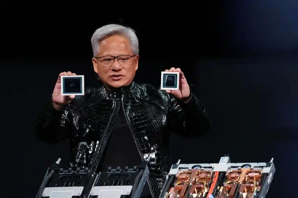
黄仁勋左手B200,右手H100

今年3月,英伟达官宣全面转向玻璃基板,Rubin身先士卒试水,硬是把玻璃基板的商业化节点快进到了今年年末。

有英伟达这只大手在前面拉,还有一只意想不到的大手在后面推。不是来自芯片产业上游,而是隔壁兄弟产业——面板。

玻璃基板在被用到芯片封装前,最大的下游应用就是显示面板。

显示面板内部呈三明治结构,两块“面包”就是玻璃基板,一块用来控制亮度,一块用来控制颜色。
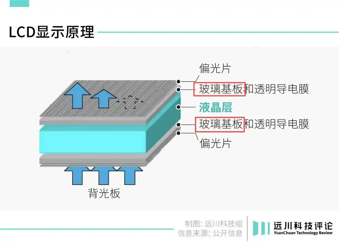
LCD面板里的玻璃基板

其中用到的精密加工技术和设备,与芯片用到的玻璃基板工艺重合度极高,夸张点说,高端产线改改就能用。

因此在玻璃基板落地这件事上,最积极的反倒是面板产业的兄弟。

比如中国台湾的面板大厂群创,最早在2019年就图谋向芯片封装转型。

正值全球面板价格战打得血肉横飞,群创眼看着招架不住,就接了台湾工研院递来的橄榄枝,共同开发基于玻璃基板的芯片封装技术,着手改造自家面板产线。

到2023年英特尔官宣玻璃基板技术,群创已经建好了全球第一条由面板产线改造的FOPLP封装产线。

隔年就拿下芯片大厂恩智浦和意法半导体的大单,还将一条闲置的5.5代面板线高价卖给了台积电,以解后者先进封装产能不足之急。

今年年初,群创的FOPLP先进封装产线月产量已拉升10倍至数千万,不仅死死抱住了台积电的大腿,据传还打入了SpaceX星链供应链。

中国台湾面板厂猛拼猛干,对岸的中国大陆对手进展速度也不遑多让。

京东方2020年就开始调研和开发玻璃基板,2024年投资近10亿元建造了试验线,今年上半年已经实现全自动化设备通线[4]。

目前已经开始给客户送样,等待测试验证,5月与康宁的合作就是为了锁定未来几年的上游特种玻璃供应,大规模量产箭在弦上。

中国大陆掌握全球面板超过六成产能,特别是高世代面板拥有全球最成熟、自动化程度最高的产线,更大的优势在于有完整的产业链上游打配合。

当前二级市场最关注的几家,例如帝尔激光、大族激光、德龙激光,就是最上游做TGV(玻璃通孔)激光微孔设备的,沃格光电则是中游做玻璃基板加工的。

中国厂商以外,韩国的三星电机、LG Innotek,日本的大日本印刷、日本电气硝子,都是玻璃基板的积极分子,也都是从面板战争中厮杀过来的熟面孔。

下有金主保需求,上有兄弟产业送温暖,让玻璃基板从被理中客严肃批判的“概念炒作”,迅速进展到“量产前夜”,券商机构一改谨慎态度,饼画得越来越大。

客观来说,目前距离玻璃基板大规模落地,还差几个技术难关要闯。

比如核心材料特种玻璃,目前只有康宁能做到11层加工而不碎裂,国内供应链最多做到3-4层[5];再比如铜电镀设备工艺不足等[5]。

根据产业链预估,玻璃基板要大规模放量,最早也得等到2027年年末。

算力的尽头是电力,但在走到这个尽头前,产业链要跨过槛,可能还得多加一个玻璃基板。

参考资料

[1] 基于玻璃基板的2.5DCoWoS 封装翘曲研究,师航波,王旭,范吉磊等

[2] 大型硅中介层单价超100美元占成本一半,AI算力芯片如何突围封装成本瓶颈?约投顾

[3] TGV玻璃穿孔完整拆解:Intel玻璃基板登场后,看懂硬门槛、2027量产倒数与台湾供应链投资地图,永丰金证券

[4] 京东方:玻璃基封装载板试验线已通线,设计产能1000片/月,未来半导体

[5] 玻璃基板行业交流,纪要研报地

本文来自微信公众号“远川科技评论”(ID:kechuangych),作者:何律衡,编辑:李墨天

Criptos en tendencia

Preguntas relacionadas

Q英特尔和台积电推动的“玻璃基板”技术,主要替代的目标分别是什么?

A英特尔提出的“玻璃核心基板”主要替代的是芯片封装中电路板与芯片之间的IC载板(如ABF材料载板),以解决因热膨胀系数不匹配导致的翘曲问题。台积电的“玻璃基板”则是希望替代位于芯片裸片层、连接计算核心与HBM的硅中介层,以大幅降低封装成本。

Q文章中提到,推动玻璃基板商业化进程突然加速的“两只大手”分别指谁?

A第一只“大手”是英伟达,其即将量产的大尺寸AI芯片(如Rubin)对载板的性能和尺寸提出了更高要求,官方宣布转向玻璃基板技术,将商业化节点提前。第二只“大手”是面板产业,以群创、京东方为代表的面板厂商利用其在玻璃基板精密加工方面的技术储备和产线,快速切入芯片封装领域,为玻璃基板量产提供了现成的产能和技术支持。

Q玻璃基板相比于传统材料(如ABF载板、硅中介层)的主要优势是什么?

A主要优势有两点:1. 热性能匹配:玻璃的热膨胀系数与硅芯片更接近,高温工作时能与芯片保持同步形变,有效防止载板翘曲,这对于大尺寸芯片至关重要。2. 成本优势:与高成本的硅中介层相比,同样尺寸的玻璃基板成本不到其一半,有助于降低高端AI芯片的封装成本。

Q中国大陆在玻璃基板产业链上有哪些主要参与者?目前面临什么技术挑战?

A主要参与者包括:上游设备商如帝尔激光、大族激光(TGV激光微孔设备),中游加工商如沃格光电,以及下游面板/封装厂商如京东方。目前面临的技术挑战主要集中在核心材料和工艺上,例如:核心特种玻璃材料(国内目前加工层数有限,约3-4层,而康宁可达11层),以及铜电镀等关键工艺和设备仍需突破。

Q根据文章和产业链信息,玻璃基板技术预计何时能实现大规模商业应用?

A根据产业链预估,玻璃基板要大规模放量,最早也得等到2027年年末。尽管英伟达等厂商的推动和面板产业的介入加速了进程,但仍需克服材料、工艺等关键技术难关,并通过客户测试验证。

Lecturas Relacionadas

In the AI Era, What's Left for Bitcoin?

As Bitcoin falls below $60,000, the author reflects on the relationship between AI and Bitcoin, seeing them as two sides of the same coin. In the AI era, the cost of generating content has plummeted, making fake text, images, and videos increasingly easy and cheap to produce. This has led to a fundamental shift: while AI dramatically lowers the cost of information production, it also undermines trust and authenticity online. What becomes truly valuable is not more content, but the ability to verify what is real—"verifiability." This perspective offers a new lens for Bitcoin. Its massive energy consumption, often criticized as wasteful, is reinterpreted. While AI burns energy to enhance "capability" and efficiency, Bitcoin burns energy to produce "verifiability." Its purpose is not to be trusted but to enable a system where no trust in intermediaries—banks, platforms, or developers—is needed. Every transaction and the entire ledger's history is secured by cryptography and a decentralized network of nodes, making it independently verifiable. AI cannot forge a transaction on the Bitcoin network because the system is designed for proof, not generation. The author draws a historical parallel to the Renaissance: the printing press drastically reduced the cost of copying knowledge, while double-entry bookkeeping reduced the cost of trust in commerce. Today, AI is the new printing press, reducing content creation costs to near zero. Blockchain, and Bitcoin as its pioneer, may be the modern equivalent of double-entry bookkeeping—a foundational technology for verifying digital asset ownership and historical records without centralized authorities. Thus, AI and blockchain are not competitors. AI lowers the cost of creation; blockchain lowers the cost of verification. In an age where AI can generate anything, true scarcity may lie not in more content, but in independently verifiable facts. Whether the market will reprice Bitcoin accordingly remains uncertain, but its core value proposition as a "machine for producing verifiability" becomes strikingly relevant.

marsbitHace 20 min(s)

In the AI Era, What's Left for Bitcoin?

marsbitHace 20 min(s)

In the Age of AI, What's Left for Bitcoin?

Author: Sevclub, Seven Research Amid Bitcoin's recent drop below $60k, the author reflects on a growing sense that AI and Bitcoin are two sides of the same coin. Today, encountering any content triggers a new default question: "Was this made by AI?" The cost of generating convincing text, images, and video is now negligible. While the internet lowered information *distribution* costs, AI is crashing information *production* costs to near zero. The consequence is a flood of content where truth and falsehood are increasingly indistinguishable. In this environment, what becomes truly valuable is not more information, but the ability to verify what is real—"verifiability." This reframes the common criticism that Bitcoin "wastes electricity." AI consumes power to produce "capability" (e.g., more powerful models). Bitcoin consumes power to produce something else: "verifiability." Bitcoin's core purpose isn't about belief or trust in any institution, developer, or even its creator. It's about enabling independent verification. Every bitcoin's origin, every transaction, and the integrity of the entire ledger are secured by mathematics, cryptography, and a global network of nodes. AI can fabricate convincing media, but it cannot falsify a transaction on the Bitcoin network. The expended energy makes篡改历史 (tampering with history) prohibitively expensive, purchasing a globally verifiable ledger. The author draws a historical parallel to the Renaissance. The printing press drastically reduced the cost of copying knowledge, while double-entry bookkeeping reduced the cost of trust in commerce—one enabled creation, the other verification. Today, AI is the new printing press, driving content production costs toward zero. The question becomes: what is this era's "double-entry bookkeeping"? Blockchain appears to be the leading candidate. It doesn't verify which news is true or which image is real, but it provides a foundational layer for independently verifying asset ownership and historical records in the digital realm without centralized authorities. Therefore, AI and blockchain are not in competition. AI lowers the cost of *generation*. Blockchain (and Bitcoin as a prime example) lowers the cost of *verification*. One creates, the other proves. Whether Bitcoin ultimately succeeds remains uncertain, facing potential challenges from quantum computing, regulation, and technical evolution. However, the author now sees it less as a "machine for making bitcoin" and more as a "machine for making verifiability." In an age where AI can generate anything, true scarcity may no longer be "more content," but "more independently verifiable facts." Whether the market will price this accordingly is a separate question.

链捕手Hace 28 min(s)

In the Age of AI, What's Left for Bitcoin?

链捕手Hace 28 min(s)

Trading

Spot

Artículos destacados

Cómo comprar WAVES

¡Bienvenido a HTX.com! Hemos hecho que comprar Waves (WAVES) sea simple y conveniente. Sigue nuestra guía paso a paso para iniciar tu viaje de criptos.Paso 1: crea tu cuenta HTXUtiliza tu correo electrónico o número de teléfono para registrarte y obtener una cuenta gratuita en HTX. Experimenta un proceso de registro sin complicaciones y desbloquea todas las funciones.Obtener mi cuentaPaso 2: ve a Comprar cripto y elige tu método de pagoTarjeta de crédito/débito: usa tu Visa o Mastercard para comprar Waves (WAVES) al instante.Saldo: utiliza fondos del saldo de tu cuenta HTX para tradear sin problemas.Terceros: hemos agregado métodos de pago populares como Google Pay y Apple Pay para mejorar la comodidad.P2P: tradear directamente con otros usuarios en HTX.Over-the-Counter (OTC): ofrecemos servicios personalizados y tipos de cambio competitivos para los traders.Paso 3: guarda tu Waves (WAVES)Después de comprar tu Waves (WAVES), guárdalo en tu cuenta HTX. Alternativamente, puedes enviarlo a otro lugar mediante transferencia blockchain o utilizarlo para tradear otras criptomonedas.Paso 4: tradear Waves (WAVES)Tradear fácilmente con Waves (WAVES) en HTX's mercado spot. Simplemente accede a tu cuenta, selecciona tu par de trading, ejecuta tus trades y monitorea en tiempo real. Ofrecemos una experiencia fácil de usar tanto para principiantes como para traders experimentados.

267 Vistas totalesPublicado en 2024.12.11Actualizado en 2026.06.02

Cómo comprar WAVES

Discusiones

Bienvenido a la comunidad de HTX. Aquí puedes mantenerte informado sobre los últimos desarrollos de la plataforma y acceder a análisis profesionales del mercado. A continuación se presentan las opiniones de los usuarios sobre el precio de WAVES (WAVES).

活动图片