SatoshiVM与IDO平台互掐,300倍神话因利益不均“闪崩”

Odaily星球日报Publicado a 2024-01-25Actualizado a 2024-01-25

Resumen

人性总是禁不起考验。

原文作者:深潮 TechFlow

SatoshiVM与IDO平台互掐,300倍神话因利益不均“闪崩”

还记得那个一天上涨 50 倍,IDO 收益 300 倍,超过 280 个知名 KOL 喊单宣传的比特币L2项目 SatoshiVM 么?

从发布第一条推特到正式启动发行,仅仅花费了 10 天,便创造了一个上亿美元市值的比特币概念热门项目。

围绕着该项目产生了大量疑问:

该项目背后的发行人是谁?为何能在短时间内调动加密领域最具影响力的超过 200 位 KOL 集体宣传?

根据 SatoshiVM 代币经济学,供应量的 15% 分配给贡献者(KOL),分配合约 0x e 77 … 5 E 00 向 250 位 KOL 发送了超过 120 万 SAVM(约 1, 200 万美元),其中 50% 已在 Uniswap 上抛售。

SatoshiVM与IDO平台互掐,300倍神话因利益不均“闪崩”

有人通过测试网中的合约发现该项目的技术方案来源于 Bool Network ,因此推测,SatoshiVM 为 Bool Network 团队所发行,但根据深潮 TechFlow 记者的查访,Bool Network 仅仅提供一种技术解决方案,Bool Network 目前专注于比特币验证层,可以服务所有比特币 Layer 2 。

也有人猜测 SatoshiVM 背后的运营全部来自于 DAOMaker 前员工创建的 IDO 平台,Ape Terminal,SatoshiVM 正是在 Ape Terminal 上进行 IDO 发行。

1 月 25 日,或因“利益纠纷”,Ape Terminal 与 SatoshiVM 团队公开吵架,相互爆光背后的“丑闻”。

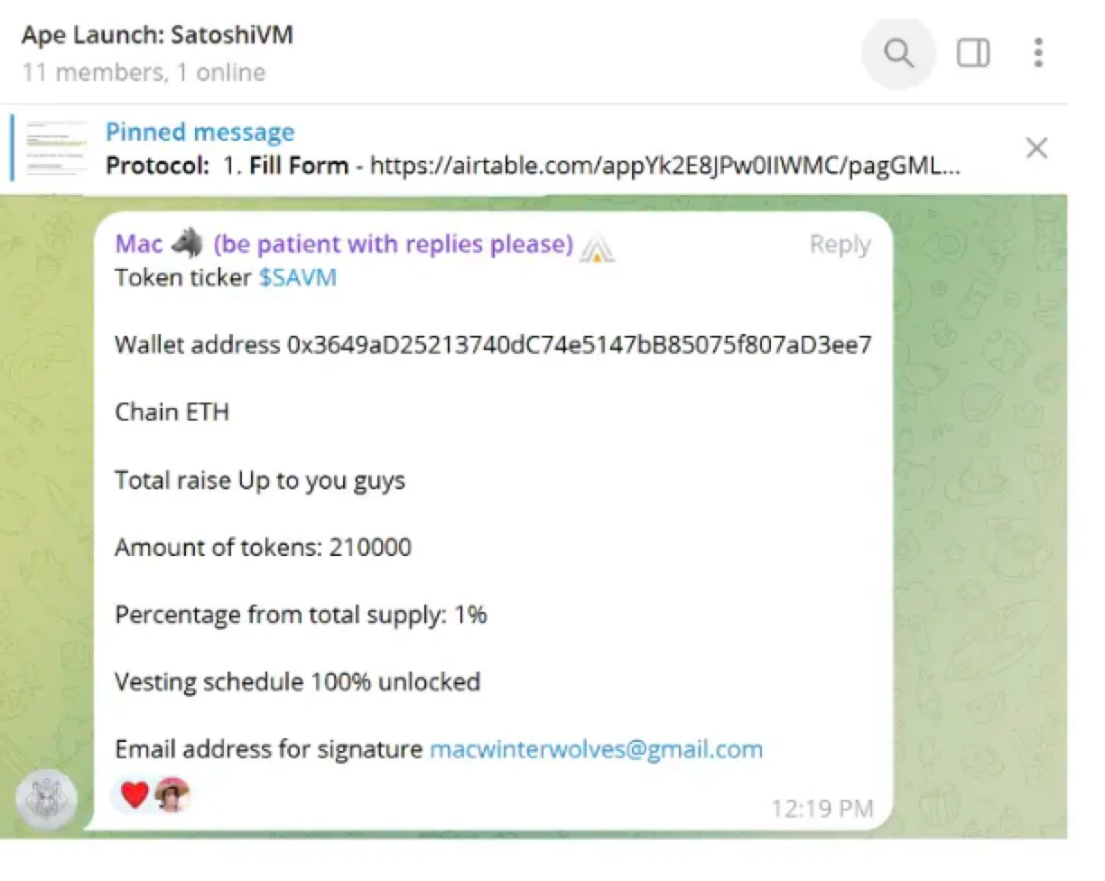
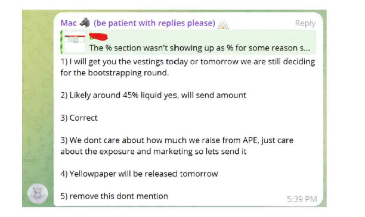
首先,由一直带头宣传 SatoshiVM,拥有 50 万粉丝的知名 KOL MacnBTC 向 Ape Terminal 发难,他称 Ape Terminal 欺骗了所有人,他们并不是公平发售,有 20 万个钱包申请参与 IDO,但每次只有 10 名获胜者,而所有获胜者都是 Ape Terminal 团队成员。此外,Ape Terminal 还收取了 25% 的手续费。

SatoshiVM与IDO平台互掐,300倍神话因利益不均“闪崩”

尽管 Ape Terminal 团队将 IDO 部分费用还给了 Satoshivm 团队,但却通过出售老鼠仓钱包赚取了数百万美元。

SatoshiVM 官方推特确认 Ape Terminal 已退还其 IDO 的 25% 费用,总共 52, 000 $SAVM已返还给 SatoshiVM 金库。

面对指责,Ape Terminal 发布声明进行反击,称 SAVM 是就由知名 KOL MacnBTC 创立的项目。

SatoshiVM与IDO平台互掐,300倍神话因利益不均“闪崩”

SatoshiVM与IDO平台互掐,300倍神话因利益不均“闪崩”

“SAVM 对于 Ape Terminal 来说是一个苦乐参半的事件, Mac 和他的 KOL 朋友们通过在自己的社区倾销而获利 2000 万美元以上。”

Ape Terminal 通过一份google 文档给出了与 mac 接触的详细信息以及清算代币的记录。

在 Ape Terminal 看来,他们则成为了 MAC 的替罪羊。

对此,MAC 回应称,他自己是 SatoshiVM 团队的顾问,并且与他们密切合作,是把 Ape Terminal 介绍给了 SatoshiVM 团队,然而在 SatoshiVM 团队取得成功后,被断章取义攻击,他并没有抢注流动性,而是另有其人。

或因撕逼事件,SAVM 代币 24 小时下跌超过 30% 。

SatoshiVM与IDO平台互掐,300倍神话因利益不均“闪崩”

天下熙熙皆为利来,天下攘攘皆为利往,加密世界同样如此,或许从一开始所有人都没预料过这个项目是如此“成功”,以至于在大方给出筹码之后,不少人又觉得自己利益被侵犯。

目前 KOL、项目方和 IDO 平台各执一词,真相或许只有他们自己知道。不过在一个强调去信任化的加密行业,错综复杂的利益纠纷中,信任本身却又显得稀缺且珍贵。

人性总是禁不起考验。

Lecturas Relacionadas

The "Impossible Triad" Is Fundamentally a Pseudo-Problem

The article argues that blockchain's fundamental limitation is not the scalability trilemma (decentralization, scalability, security), which has been largely solved, but the lack of **privacy** and, until recently, clear **legitimacy**. Blockchain is described as a slow, expensive, globally shared computer whose core value is censorship resistance and verifiability. While ideal for native digital assets like money (e.g., stablecoins), its default transparency acts as a **tax**, exposing all transactions and enabling MEV extraction, which deters serious institutional capital. Simultaneously, its permissionless nature created regulatory ambiguity. The piece contends that **privacy** is the missing critical feature. It rejects the false choice between total transparency and complete anonymity. Modern cryptography (like zero-knowledge proofs) enables **compliant privacy**: users can prove facts (solvency, KYC status, compliance) without revealing the underlying sensitive data (specific holdings, identities). This preserves auditability for regulators and eliminates the leak of financial information. With recent regulatory progress (e.g., the GENIUS Act) addressing legitimacy, adding default, provably compliant privacy becomes a pure upgrade. It transforms blockchain from a costly, public ledger into a confidential settlement layer, finally bridging the gap to mainstream institutional and individual adoption of on-chain finance.

链捕手Hace 11 hora(s)

The "Impossible Triad" Is Fundamentally a Pseudo-Problem

链捕手Hace 11 hora(s)

Optical Chips: Collective Capacity Expansion

The global optical chip industry is experiencing a massive wave of expansion driven by surging AI data center demand. Major players across the US, Japan, Europe, and China are aggressively investing to ramp up production capacity. In the US, Coherent is expanding its 6-inch Indium Phosphide (InP) semiconductor fab in Texas, supported by CHIPS Act funding and a $2 billion strategic investment from NVIDIA. Lumentum is building a new factory for InP optical devices, and Nokia is scaling its advanced photonic chip packaging and testing capabilities. NVIDIA's investments aim to secure future supply of critical lasers and optical interconnect products for AI infrastructure. Japan's JX Advanced Metals, a leading InP substrate supplier, plans a multi-billion yen investment to increase its capacity 7-10 times, strengthening its grip on the crucial upstream materials market. In Europe, IQE and Tower Semiconductor settled a patent dispute and signed a multi-year InP epitaxial wafer supply agreement, highlighting that next-generation silicon photonics platforms will integrate high-performance InP components. STMicroelectronics and Sivers Semiconductors are also expanding silicon photonics production and partnerships. China is rapidly building out its domestic supply chain. Dongshan Precision's subsidiary, Source Photonics, announced a $12 billion project to expand optical chip and module production. Companies like Sanan Optoelectronics and Yunnan Germanium are scaling up InP chip manufacturing and substrate production, moving towards vertical integration from materials to modules. While debate continues around the exact future architecture—whether CPO (Co-Packaged Optics), NPO, or pluggables will dominate—analysts like Morgan Stanley argue the underlying driver is unchangeable: the explosive growth in bandwidth demand. This will inevitably increase the volume of optical engines, lasers, and related content per GPU, regardless of the final technical path. The competition for "more light" in the AI era has intensified into a global, full-chain capacity race.

marsbitHace 14 hora(s)

Optical Chips: Collective Capacity Expansion

marsbitHace 14 hora(s)

Trading

Spot
Futuros
活动图片